EP0973261B1 - Circuit actif de tirage-haut pour signaux drain ouvert - Google Patents
Circuit actif de tirage-haut pour signaux drain ouvert Download PDFInfo
- Publication number
- EP0973261B1 EP0973261B1 EP99113598A EP99113598A EP0973261B1 EP 0973261 B1 EP0973261 B1 EP 0973261B1 EP 99113598 A EP99113598 A EP 99113598A EP 99113598 A EP99113598 A EP 99113598A EP 0973261 B1 EP0973261 B1 EP 0973261B1
- Authority
- EP
- European Patent Office
- Prior art keywords
- current
- signal line
- circuitry
- pullup
- voltage
- Prior art date
- Legal status (The legal status is an assumption and is not a legal conclusion. Google has not performed a legal analysis and makes no representation as to the accuracy of the status listed.)
- Expired - Lifetime
Links
- 239000003990 capacitor Substances 0.000 claims description 10
- 238000001514 detection method Methods 0.000 claims description 7
- 238000012544 monitoring process Methods 0.000 claims description 5
- 230000003071 parasitic effect Effects 0.000 description 14
- 238000010586 diagram Methods 0.000 description 7
- 238000000034 method Methods 0.000 description 7
- 230000008859 change Effects 0.000 description 5
- 238000004891 communication Methods 0.000 description 5
- 230000002829 reductive effect Effects 0.000 description 5
- 230000004044 response Effects 0.000 description 4
- 230000011664 signaling Effects 0.000 description 4
- 230000001276 controlling effect Effects 0.000 description 3
- 230000000630 rising effect Effects 0.000 description 3
- 230000007704 transition Effects 0.000 description 3
- 230000002411 adverse Effects 0.000 description 2
- 238000013459 approach Methods 0.000 description 2
- 230000000694 effects Effects 0.000 description 2
- 238000004904 shortening Methods 0.000 description 2
- 239000007787 solid Substances 0.000 description 2
- 230000005540 biological transmission Effects 0.000 description 1
- 230000003247 decreasing effect Effects 0.000 description 1
- 230000001419 dependent effect Effects 0.000 description 1
- 238000007599 discharging Methods 0.000 description 1
- 230000005669 field effect Effects 0.000 description 1
- 230000000670 limiting effect Effects 0.000 description 1
- 230000002093 peripheral effect Effects 0.000 description 1
- 230000009467 reduction Effects 0.000 description 1
- 230000001105 regulatory effect Effects 0.000 description 1
- 230000002441 reversible effect Effects 0.000 description 1
- 230000035945 sensitivity Effects 0.000 description 1
- 238000012546 transfer Methods 0.000 description 1
Images


Classifications
-
- H—ELECTRICITY
- H03—ELECTRONIC CIRCUITRY
- H03K—PULSE TECHNIQUE
- H03K19/00—Logic circuits, i.e. having at least two inputs acting on one output; Inverting circuits
- H03K19/01—Modifications for accelerating switching
- H03K19/013—Modifications for accelerating switching in bipolar transistor circuits
- H03K19/0136—Modifications for accelerating switching in bipolar transistor circuits by means of a pull-up or down element
-
- H—ELECTRICITY
- H03—ELECTRONIC CIRCUITRY
- H03K—PULSE TECHNIQUE
- H03K19/00—Logic circuits, i.e. having at least two inputs acting on one output; Inverting circuits
- H03K19/01—Modifications for accelerating switching
- H03K19/017—Modifications for accelerating switching in field-effect transistor circuits
- H03K19/01707—Modifications for accelerating switching in field-effect transistor circuits in asynchronous circuits
- H03K19/01721—Modifications for accelerating switching in field-effect transistor circuits in asynchronous circuits by means of a pull-up or down element
Definitions
- the present invention relates to methods and circuitry for increasing communication speeds in systems employing open-drain or open-collector circuitry for driving a signal line, and more particularly methods and circuitry for providing slew rate sensitive, hysteretic, active pullup.
- Open-drain terminology is used extensively throughout the description which follows. Although “open-drain” may imply the use of field effect transistors, such as MOSFETs, one of skill in the art will recognize that other types of transistors, such as bipolar transistors may be used as well. Thus, it is to be understood that the open-drain terminology is used herein as a matter of convenience, and that the terminology specifically includes open-collector type circuits. Furthermore, it is to be understood that the invention may be practiced using other than MOSFET transistors and that “transistor” specifically includes such other suitable types of transistors.
- Open-drain circuitry is commonly used to interconnect electronic devices by way of a common bus or signal line.
- the Inter-Integrated Circuit bus (I 2 C), the System Management Bus (SMBus), ACCESS.bus, and Apple Desktop Bus (ADB) are a few of the inter-device communication protocols that use an open-drain architecture.
- Open-drain signals are also used within computer systems for lines that may be driven by more than one source, e.g., an interrupt input of a microprocessor.
- a device sends signals on an open-drain signal line by controlling a transistor coupled between the open-drain signal line and ground.
- the transistor which is used as a switch, is an N-channel MOSFET, but other types of transistors are also suitable for this purpose.
- the transistor may be internal to the device, or the device may have a terminal for controlling an external transistor.
- the signal line When the device causes the transistor to be ON, the signal line is coupled to ground, causing its voltage to be pulled down to a LOW state or level, e.g., less than about 0.4 volts. Conversely, when all devices cause their corresponding driver transistors to be OFF, the signal line is biased to a HIGH state, e.g., 5 volts, by pullup circuitry connected between the signal line and a power supply rail.
- the speed at which signals may be transmitted on an open-drain signal line is dependent on how rapidly the signal line can be cycled between LOW and HIGH levels. Because of parasitic capacitance associated with the signal line, the rate at which it may be switched is determined by how rapidly the parasitic capacitance may be charged and discharged. Other factors being equal, an increase in parasitic capacitance slows the charge and discharge rates, and lowers the maximum signaling rate. Therefore, many open-drain based interconnection standards specify a maximum signal line capacitance, typically a few hundred picofarads, to ensure adequate performance.
- Another factor determining the rate at which the parasitic capacitance is charged and discharged is the resistance in the charge and discharge current paths. Since the resistance of an output transistor is typically very small when the transistor is ON, the parasitic capacitance may be discharged very rapidly, and the transition from HIGH to LOW occurs quickly. However, the parasitic capacitance is charged by pullup current provided by some form of pullup circuitry.
- the pullup circuitry is simply a pullup resistor coupled between the signal line and a positive supply rail. Because the resistance of a pullup resistor is typically much larger than the ON resistance of a driver transistor, the rate at which the parasitic capacitance may be charged is much slower than the rate at which it may be discharged. The signal rise time is, therefore, much slower than the signal fall time.
- One technique for shortening signal rise time is to use a smaller valued pullup resistor. Using a smaller resistance increases the available pullup current, so that any parasitic capacitance may be charged more quickly when all driver transistors are OFF. However, reducing pullup resistance may have adverse effects on circuit operation.
- reducing the value of the pullup resistor increases current flow from V cc to ground when a driver transistor is ON.
- This increased current represents wasted electrical power, which may be an important consideration in low power applications such as battery powered devices.
- the increased current also increases the voltage drop across the driver transistor, thereby raising the signal line voltage and reducing the noise margin associated with a LOW signal line level.
- DE-37-38-800-A discloses a data transfer circuit comprising a capacitor that utilizes a change in the voltage potential of a data bus to provide a pulse to pulse transistor in order to reduce signal rise time of the circuit.
- the output of the capacitor is a signal representative of the capacitor's charging or discharging.
- pullup current is provided by a variable current source in which the available pullup current is a function of a voltage level on the signal line.
- the available pullup current is increased when the signal line voltage indicates that the signal line is not being pulled LOW.
- the additional pullup current is provided whenever a signal on the signal line exceeds a threshold level.
- circuitry is provided to monitor the slew rate (dV/dt) of the signal, and higher pullup current is provided only when the signal exceeds the threshold and the slew rate is positive, such as during a LOW-to-HIGH signal transition.
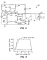
- FIGS. 1A through 1C are simplified schematic diagrams of previously known circuitry for implementing signal lines using an open-drain architecture.
- Device 16 represents a device coupled to signal line 11 and may be anything from an integrated circuit to a computer peripheral.
- Device 16 includes driver transistor 14 which may be turned ON or OFF by additional circuitry within device 16 (not shown). Alternatively, device 16 may include a terminal for controlling an external driver transistor. It should be noted that in the schematics of FIGS. 1, 3, and 5 only one device is shown connected to signal line 11; however, one skilled in the art will understand that there may be more than one such device.
- Capacitor 18 represents the parasitic capacitance associated with signal line 11, including stray capacitance associated with signal line 11 itself, as well as with the drivers and receivers coupled to signal line 11.
- Driver transistor 14 is connected between signal line 11 and ground so that device 16 may actively pull signal line 11 LOW by turning driver transistor 14 ON. Since any similar device connected to signal line 11 is capable of pulling it LOW, the signal line can only be HIGH when driver transistor 14 associated with each device is turned OFF.
- any device connected to signal line 11 may selectively drive the signal line LOW by turning ON the driver transistor associated with the device. Conversely, when transistor 14 is OFF in all devices connected to signal line 11, pullup circuitry connected to the signal line biases the signal line HIGH.
- pullup circuitry 10 consists of pullup resistor 12 connected between V cc and signal line 11. When transistor 14 is switched OFF, current flows through pullup resistor 12 to signal line 11, pulling it up to V cc .
- pullup resistor 12 has a value on the order of a few thousand ohms.
- a typical signal on signal line 11 of FIG. 1A is shown by the solid trace in FIG. 2A.
- transistor 14 Prior to time t 0 , transistor 14 is OFF, and signal line 11 is HIGH.
- transistor 14 is turned ON by device 16, providing a low resistance path between signal line 11 and ground. This rapidly discharges capacitance 18 to ground, pulling signal line 11 LOW at time t 1 .
- the interval between time to and t 1 i.e., the time needed for signal line 11 to reach a LOW level after transistor 14 is turned ON, is referred to as the fall time (t f ).
- transistor 14 is turned OFF by device 16.
- Current through pullup resistor 12 charges capacitance 18 causing the voltage on signal line 11 to rise, pulling signal line 11 HIGH at time t 3 .
- the interval between time t 2 and t 3 i.e., the time needed for signal line 11 to reach a HIGH level after transistor 14 is turned OFF, is referred to as the rise time (t r ).
- the circuit of FIG. 1A is a resistor-capacitor (RC) circuit.
- the response of RC circuits exhibit a characteristic exponential waveform over a time determined by the time constant of the circuit, wherein the time constant is the product of circuit capacitance and the resistance in the current path. Circuits having a larger time constant have longer rise and fall times.
- pullup resistor 12 In a typical open-drain system, the value of pullup resistor 12 is much larger than the ON-resistance of driver transistor 14. This causes signal rise time (t r ) to be many times longer than the signal fall time (t f ). Since the rate at which data may be transmitted on signal line 11 is largely limited by the rise time (t r ), techniques for increasing data transmission rates have generally focused on shortening the rise time in open-drain systems.
- rise time may be reduced by reducing the value of pullup resistor 12. This would reduce the RC time constant of the circuit, thereby providing a shorter rise time. Since reducing pullup resistance may adversely affect power consumption and noise susceptibility, other techniques have been developed to reduce signal rise time.
- Open-drain circuitry 20 includes pullup resistor 12, transistor 14, and capacitance 18 which correspond to like elements of FIG. 1A.
- Pullup circuitry 20 also includes additional pullup resistor 12a, which may be selectively connected in parallel with pullup resistor 12 by means of switch 13.
- Switch 13 which may be, for example, a CD4066 CMOS switch, is controlled by a level on control input 15, such that a LOW signal at control input 15 causes switch 13 to be OFF, while a HIGH signal causes the switch to be ON.
- the decrease in pullup resistance caused by turning on switch 13 is a function of the relative values of resistors 12 and 12a. For example, if the values of resistors 12 and 12a are equal, the available pullup resistance is effectively halved when switch 13 is turned ON. This reduces the RC time constant associated with pulling signal line 11 high, resulting in a shorter rise time (t r ).
- FIGS. 2A and 2B The response of pullup circuitry 20 is shown in FIGS. 2A and 2B. From time to to t 1 , the circuit response and waveform are nearly identical to those of FIG. 1A. At time t 2 transistor 14 is turned OFF, and the voltage on signal line 11 begins to rise, following the same waveform as the solid trace corresponding to the circuit of FIG. 1A. At time t 4 signal line 11 reaches a voltage of about one-half V cc and switch 13 turns ON, greatly reducing pullup resistance. The reduced pullup resistance reduces the RC time constant and signal line voltage rises much faster, as shown by the dashed line in FIG. 2A. The corresponding pullup current is shown by the dashed line in FIG. 2B.
- pullup resistor 12 may be made large enough to address the concerns about excess current, power consumption, and noise margin discussed hereinabove, and resistor 12a may be made small enough to provide adequate pullup performance.
- FIG. 1C A third alternative pullup scheme is shown in FIG. 1C, wherein pullup current for signal line 11 is provided by constant current source 32.
- constant current source 32 In the circuitry of FIGS. 1A, and 1B, pullup current drops as the voltage on signal line 11 rises, giving the response waveform its characteristic exponential shape.
- Using a constant current source ensures that the pullup current, and hence the charging rate of capacitance 18, remains nearly constant, resulting in a near linear increase in signal line voltage. This is illustrated by the dotted line in FIGS. 2A and 2B. Note, that as signal line voltages approach that of the supply rail, pullup current begins to drop due to reduced operating headroom for constant current source 32.
- circuitry of FIGS. 1B and 1C are effective at reducing signal rise times in open-drain circuits, maximum signaling rates are still limited to less than about 1 MHz using these types of pullup circuits.
- care must be taken to keep stray capacitance to a very small value, for example, by limiting the length of signal line 11, or the number of devices connected to signal line 11.
- Pullup circuitry 40 includes transistors 41-44, and resistors 45-48. Transistors 41 and 42 are connected to form a current mirror such that collector current I 2 of transistor 42 is approximately proportional to collector current I 1 of transistor 41. If signal line 11 is LOW, transistor 43 is biased OFF, and the current I 1 is determined by the values of resistors 45 and 46.
- FIG. 4 also shows a dashed line which represents a load-line corresponding to the ON resistance of driver transistor 14. This is an indication of how much current transistor 14 can sink at any given signal line voltage, i.e., the available "pulldown" current.
- the pullup current In designing a pullup circuit such as that in FIG. 3A, it is important that the pullup current always remain less than the current transistor 14 can sink. Otherwise, transistor 14 cannot sink enough-current to pull signal line 11 LOW.
- pullup circuitry 60 provides additional pullup current only when signal line 11 is not being pulled LOW.
- Pullup circuitry 60 functions in a manner analogous to the circuitry of FIG. 3.
- Transistors 61 and 62 form a current mirror, wherein the current through transistor 62 provides pullup current to signal line 11.
- Transistor 63 causes an increase in pullup current I 2 as signal line voltage increases, and transistor 64 limits the maximum pullup current to an acceptable level.
- pullup Circuitry 60 includes additional circuitry to create hysteresis in the current-voltage characteristic of the pullup circuit as is shown in FIG. 6.
- Operational amplifier 67 in conjunction with capacitor 68 and resistor 69 form a differentiator that monitors the change in voltage on signal line 11.
- the output of operational amplifier 67 is a signal indicative of how fast the signal line voltage is changing, i.e., the slew rate.
- comparator 53 out puts a signal turning ON transistor 54.
- the threshold level is provided at the '+' input of comparator 53 by diodes 51 and 52. Turning transistor 54 ON enables current I 3 to flow through transistor 63, providing increased pullup current in a manner analogous to that described in connection with FIG. 3.
- pullup circuitry 60 provides additional pullup current only when the voltage on signal line 11 is rising, the pullup current may exceed the pull-down current load line represented by a dashed line in FIG. 6. This enables the rise in pullup current to be very rapid. Indeed, as long as the increased current is only provided when signal line 11 is not being pulled down, the change in pullup current may be an instantaneous step change.
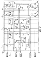
- Pullup circuitry 70 includes four basic sections of circuitry: voltage level detection circuitry 71 for monitoring the voltage level on signal line 11; slew rate detection circuitry 77 for monitoring the rate at which the signal line voltage is changing; nominal pullup current circuitry 88 for providing pullup current when the signal line is stable or being pulled down; and high pullup current circuitry 95 for providing increased pullup current when needed.
- pullup circuitry 70 includes circuitry for implementing a low power mode suitable for use in battery powered systems.
- Additional voltages and signals are provided to the circuitry of FIG. 7 by circuitry not shown therein.
- voltage regulating circuitry (not shown) provides voltages to BIASH and BIASL for biasing, respectively, the high-side and low-side MOSFET current sources of FIG. 7, and provides a voltage reference to VREF.
- Additional circuitry provides a shutdown signal to -SHDN.
- SGNL is connected to the signal line, e.g., signal line 11 of FIG. 5.
- voltage level detection circuitry 71 includes a differential amplifier 72 which splits current I 1 into currents I 1a and I 1b according to the voltage at SGNL relative to the voltage at VREF (a voltage reference).
- Current I 1a is mirrored by current mirror 73 to provide current I 2 tending to pull node 74 to ground.
- current I 1b is mirrored by current mirrors 75 and 76 to provide current I 3 tending to pull node 74 up to V cc
- constant current I 4 is provided by transistors 78, 79, and 80 in conjunction with current mirror 82.
- Current I 4 is mirrored by current mirrors 81 and 82 to provide currents I 5 and I 6 , respectively.
- current mirror 81 has a gain of about twice that of current mirror 82, so that current I 5 is normally about twice as large as I 6 , and node 83 is pulled high.
- Capacitor 84 blocks any DC component of SGNL voltage, but passes the AC component through to current mirror 82. Specifically, an increasing SGNL voltage adds to the current flowing into current mirror 82, thereby increasing current I 6 . At the same time, the current flowing through current mirror 81 is reduced, thereby decreasing current I 5 . A sufficiently rapid positive change in SGNL voltage causes current I 6 to be larger than I 5 , pulling node 83 low.
- Capacitor 84 and resistor 85 are selected to provide adequate sensitivity to slew rate without being overly sensitive to noise on the signal line (SGNL). Suitable values for capacitor 84 and resistor 85 are about 2pF and about 187 ⁇ , respectively.
- Nominal pullup current circuitry 88 provides pullup current when the SGNL line is stable or being pulled down.
- Circuitry 88 includes current mirror 89 having an output current coupled back to SGNL, and an input current set by transistors 90 and 91.
- Transistor 92 may be turned OFF by a low level on the -SHDN terminal, isolating transistor 90, and thereby reducing the input current to current mirror 89.
- This circuit architecture provides a means of reducing pullup current to a shutdown level when appropriate. For example, when the signal line is high, and has been high for an extended period of time, pullup current may be reduced to a low level to conserve power in a battery powered device.
- pullup circuitry 88 is designed such that normal pullup current is about 250 ⁇ A when -SHDN is HIGH, and low power pullup current is about 100 ⁇ A when -SHDN is LOW.
- pullup current boost circuitry 95 provides additional pullup current when the voltage at SGNL is above a threshold voltage, as determined by voltage level detection circuitry 71, and exceeds a minimum positive slew rate, as determined by slew rate detection circuitry 77.
- the inputs to gate 96 are coupled to node 74, the output of voltage level detector 71, and node 83, the output of slew rate detector 77.
- node 74 is pulled LOW whenever the voltage level at SGNL exceeds VREF, and node 83 is pulled LOW whenever the voltage slew rate at SGNL becomes sufficiently large.
- the output of gate 96 is HIGH only when both inputs are LOW. Thus, the output of gate 96 is high when the conditions for supplying boosted pullup current are satisfied.
- a HIGH output of gate 96 turns transistor 97 OFF and transistor 98 ON, thereby enabling a constant current source comprising transistor 99 and current mirror 100.
- the output of current mirror 100 is connected in parallel with the output of current mirror 89, so as to provide boosted pullup current.
- the output current of current mirror 100 is about 1.7 mA.
- Transistor 101 provides an additional source of input current for current mirror 89, increasing its output current. Preferably, turning ON transistor 101 increases the output of current mirror 89 to about 300 ⁇ A.
- pullup current is boosted from about 250 ⁇ A to about 2mA, thereby significantly reducing signal rise time
Landscapes
- Physics & Mathematics (AREA)
- Engineering & Computer Science (AREA)
- Computer Hardware Design (AREA)
- Computing Systems (AREA)
- General Engineering & Computer Science (AREA)
- Mathematical Physics (AREA)
- Electronic Switches (AREA)
- Logic Circuits (AREA)
Claims (6)
- Circuit pour, tirage haut d'une ligne de signal drain ouvert, le circuit comprenant :un circuit de surveillance de niveau (71) pour produire un premier signal indicatif d'une tension sur la ligne de signal drain ouvert (11) ;un circuit de surveillance de taux de dérive (77) pour produire un second signal indicatif d'un taux de dérive de la tension sur la ligne de signal (11);une première source de courant pour produire un courant de tirage haut sur la ligne de signal (11) ; etun circuit de commande pour commander le courant de tirage haut en réponse aux premier et second signaux, dans lequel le circuit de surveillance de niveau (71) comprend un premier comparateur, dans lequel le circuit de détection de taux de dérive (77) comprend un condensateur couplé à un second comparateur, dans lequel le premier signal indique que la tension sur la ligne de signal (11) excède une tension prédéterminée et dans lequel le second signal indique qu'un taux de dérive de la tension sur la ligne de signal (11) excède un taux de dérive prédéterminé.
- Circuit selon la revendication 1, dans lequel le circuit de commande comprend un commutateur qui est activé en réponse aux premier et second signaux.
- Circuit selon la revendication 2, dans lequel la première source de courant sur la ligne de signal comprend une résistance.
- Circuit selon la revendication 2, dans lequel la première source de courant sur la ligne de signal comprend une source de courant constant.
- Circuit selon la revendication 2, comprenant en outre une seconde source de courant pour produire un courant de tirage haut sur la ligne de signal indépendamment des premier et second signaux.
- Circuit selon la revendication 5, dans lequel la seconde source de courant comprend un circuit pour réduire la quantité de courant de tirage haut en réponse à un signal de coupure.
Applications Claiming Priority (2)
| Application Number | Priority Date | Filing Date | Title |
|---|---|---|---|
| US116309 | 1987-11-04 | ||
| US09/116,309 US6356140B1 (en) | 1998-07-15 | 1998-07-15 | Active pullup circuitry for open-drain signals |
Publications (3)
| Publication Number | Publication Date |
|---|---|
| EP0973261A2 EP0973261A2 (fr) | 2000-01-19 |
| EP0973261A3 EP0973261A3 (fr) | 2000-05-24 |
| EP0973261B1 true EP0973261B1 (fr) | 2007-12-26 |
Family
ID=22366421
Family Applications (1)
| Application Number | Title | Priority Date | Filing Date |
|---|---|---|---|
| EP99113598A Expired - Lifetime EP0973261B1 (fr) | 1998-07-15 | 1999-07-09 | Circuit actif de tirage-haut pour signaux drain ouvert |
Country Status (5)
| Country | Link |
|---|---|
| US (2) | US6356140B1 (fr) |
| EP (1) | EP0973261B1 (fr) |
| JP (1) | JP3403976B2 (fr) |
| DE (1) | DE69937817T2 (fr) |
| TW (1) | TW439359B (fr) |
Cited By (1)
| Publication number | Priority date | Publication date | Assignee | Title |
|---|---|---|---|---|
| DE102016119927A1 (de) | 2016-10-19 | 2018-04-19 | IMMS Institut für Mikroelektronik- und Mechatronik-Systeme gemeinnützige GmbH (IMMS GmbH) | Schaltungsanordnung zur Bereitstellung der Ladeenergie für einen Pegelwechsel auf einem Signalbus, Verfahren zur Kalibrierung und Signalübertragungssystem |
Families Citing this family (26)
| Publication number | Priority date | Publication date | Assignee | Title |
|---|---|---|---|---|
| DE19914466C1 (de) * | 1999-03-30 | 2000-09-14 | Siemens Ag | Treiberstufe zum Schalten einer Last |
| DE19920465C1 (de) * | 1999-05-04 | 2000-11-02 | Siemens Ag | Verfahren zur Open-Load-Diagnose einer Schaltstufe |
| EP1213655B1 (fr) * | 2000-12-11 | 2011-08-24 | Linear Technology Corporation | Circuit et procédé d'interconnexion de systèmes bus |
| DE10118863A1 (de) | 2001-04-18 | 2002-10-31 | Infineon Technologies Ag | Elektrische Schaltung |
| US6653863B1 (en) * | 2002-03-25 | 2003-11-25 | Hewlett-Packard Development Company, L.P. | Method and apparatus for improving bus capacity |
| US7348803B2 (en) * | 2005-06-24 | 2008-03-25 | Integrated Electronic Solutions Pty. Ltd. | Bi-directional bus buffer |
| DE102005050692A1 (de) * | 2005-10-18 | 2007-04-19 | Siemens Ag | Funkmodul und Schaltungsanordnung mit einem Funkmodul |
| US20070250652A1 (en) * | 2006-04-24 | 2007-10-25 | Atmel Corporation | High speed dual-wire communications device requiring no passive pullup components |
| US7446606B2 (en) * | 2006-05-31 | 2008-11-04 | Texas Instruments Incorporated | Methods and apparatus to provide slew enhancement for low power amplifiers |
| US7546817B2 (en) * | 2006-07-21 | 2009-06-16 | Radio Systems Corporation | Animal containment transmitter system |
| US7840734B2 (en) * | 2006-12-21 | 2010-11-23 | Hendon Semiconductors Pty Ltd. | Simple bus buffer |
| US7548822B2 (en) * | 2007-07-13 | 2009-06-16 | International Business Machines Corporation | Apparatus and method for determining the slew rate of a signal produced by an integrated circuit |
| US7692450B2 (en) * | 2007-12-17 | 2010-04-06 | Intersil Americas Inc. | Bi-directional buffer with level shifting |
| US7737727B2 (en) * | 2007-12-17 | 2010-06-15 | Intersil Americas Inc. | Bi-directional buffer for open-drain or open-collector bus |
| US7990128B2 (en) * | 2008-04-25 | 2011-08-02 | Infineon Technologies Ag | Circuit and method for pulling a potential at a node towards a feed potential |
| US7639045B2 (en) * | 2008-05-23 | 2009-12-29 | Intersil Americas Inc. | Bi-directional buffer and method for bi-directional buffering that reduce glitches due to feedback |
| US9183713B2 (en) | 2011-02-22 | 2015-11-10 | Kelly Research Corp. | Perimeter security system |
| JP6001876B2 (ja) * | 2012-02-24 | 2016-10-05 | ラピスセミコンダクタ株式会社 | 基準電圧中継回路 |
| US9030228B1 (en) * | 2013-12-03 | 2015-05-12 | Atmel Corporation | Intelligent current drive for bus lines |
| US20150205341A1 (en) * | 2014-01-22 | 2015-07-23 | Microsemi Corp. - Analog Mixed Signal Group, Ltd. | Bus energy consumption reduction apparatus and method |
| JP6027046B2 (ja) * | 2014-04-14 | 2016-11-16 | 株式会社日本自動車部品総合研究所 | 通信システム |
| CN105227174B (zh) * | 2015-10-12 | 2018-03-02 | 上海斐讯数据通信技术有限公司 | 支持不同有效电平数字量输入信号的检测系统及电子设备 |
| JP6880663B2 (ja) | 2016-11-14 | 2021-06-02 | セイコーエプソン株式会社 | データ通信システム及び半導体装置 |
| CN108647171B (zh) * | 2018-05-25 | 2024-02-13 | 深圳市度信科技有限公司 | 一种信号斜率控制系统和方法 |
| US11068038B2 (en) * | 2019-09-20 | 2021-07-20 | Dell Products L.P. | System and method for using current slew-rate telemetry in an information handling system |
| TWI876760B (zh) * | 2022-12-23 | 2025-03-11 | 立錡科技股份有限公司 | 上拉電壓偵測電路與上拉電壓偵測方法 |
Family Cites Families (8)
| Publication number | Priority date | Publication date | Assignee | Title |
|---|---|---|---|---|
| JPH0720060B2 (ja) * | 1985-08-14 | 1995-03-06 | 株式会社東芝 | 出力回路装置 |
| DE3738800A1 (de) | 1987-11-14 | 1989-05-24 | Philips Patentverwaltung | Datenuebertragungssystem |
| JP3251661B2 (ja) * | 1991-10-15 | 2002-01-28 | テキサス インスツルメンツ インコーポレイテツド | 制御されたスルー・レートを有するcmosバッファ回路 |
| JP3142018B2 (ja) * | 1992-03-12 | 2001-03-07 | 日本テキサス・インスツルメンツ株式会社 | 負荷駆動回路 |
| US5598119A (en) | 1995-04-05 | 1997-01-28 | Hewlett-Packard Company | Method and apparatus for a load adaptive pad driver |
| CA2193507C (fr) * | 1995-05-17 | 1999-08-10 | John Grosspietsch | Dispositif et procede de reaction positive a faible puissance |
| US5877647A (en) * | 1995-10-16 | 1999-03-02 | Texas Instruments Incorporated | CMOS output buffer with slew rate control |
| JP3592423B2 (ja) * | 1996-01-26 | 2004-11-24 | 株式会社ルネサステクノロジ | 半導体集積回路装置 |
-
1998
- 1998-07-15 US US09/116,309 patent/US6356140B1/en not_active Expired - Lifetime
-
1999
- 1999-06-10 TW TW088109700A patent/TW439359B/zh not_active IP Right Cessation
- 1999-07-09 EP EP99113598A patent/EP0973261B1/fr not_active Expired - Lifetime
- 1999-07-09 DE DE69937817T patent/DE69937817T2/de not_active Expired - Lifetime
- 1999-07-13 JP JP19942299A patent/JP3403976B2/ja not_active Expired - Lifetime
-
2001
- 2001-12-18 US US10/028,243 patent/US6650174B2/en not_active Expired - Lifetime
Cited By (2)
| Publication number | Priority date | Publication date | Assignee | Title |
|---|---|---|---|---|
| DE102016119927A1 (de) | 2016-10-19 | 2018-04-19 | IMMS Institut für Mikroelektronik- und Mechatronik-Systeme gemeinnützige GmbH (IMMS GmbH) | Schaltungsanordnung zur Bereitstellung der Ladeenergie für einen Pegelwechsel auf einem Signalbus, Verfahren zur Kalibrierung und Signalübertragungssystem |
| DE102016119927B4 (de) | 2016-10-19 | 2023-03-09 | IMMS Institut für Mikroelektronik- und Mechatronik-Systeme gemeinnützige GmbH (IMMS GmbH) | Schaltungsanordnung zur Bereitstellung der Ladeenergie für einen Pegelwechsel auf einem Signalbus, Verfahren zur Kalibrierung und Signalübertragungssystem |
Also Published As
| Publication number | Publication date |
|---|---|
| US20020053905A1 (en) | 2002-05-09 |
| JP3403976B2 (ja) | 2003-05-06 |
| DE69937817T2 (de) | 2008-04-30 |
| US6356140B1 (en) | 2002-03-12 |
| JP2000101407A (ja) | 2000-04-07 |
| US6650174B2 (en) | 2003-11-18 |
| TW439359B (en) | 2001-06-07 |
| EP0973261A3 (fr) | 2000-05-24 |
| DE69937817D1 (de) | 2008-02-07 |
| EP0973261A2 (fr) | 2000-01-19 |
Similar Documents
| Publication | Publication Date | Title |
|---|---|---|
| EP0973261B1 (fr) | Circuit actif de tirage-haut pour signaux drain ouvert | |
| JP3306344B2 (ja) | 電圧制御及び電流制限を行うソフト・スタート・スイッチ | |
| US5541799A (en) | Reducing the natural current limit in a power MOS device by reducing the gate-source voltage | |
| US6204654B1 (en) | Dynamically boosted current source circuit | |
| US20030095368A1 (en) | Inrush current control method using a dual current limit power switch | |
| US7239185B2 (en) | Driver circuit connected to pulse shaping circuitry | |
| US7180330B2 (en) | Output circuit | |
| EP0422391B1 (fr) | Circuit d'attaque CMOS | |
| US6366114B1 (en) | Output buffer with control circuitry | |
| EP1371199A2 (fr) | Circuit de commande de ligne a sortie de source de courant et faible sensibilite aux variations de charge | |
| US6891708B2 (en) | Reduced current and power consumption structure of drive circuit | |
| US20050151522A1 (en) | Constant-voltage power supply circuit | |
| JP3608199B2 (ja) | Ic間のインターフェースシステム、及びic | |
| US6518804B2 (en) | Semiconductor integrated circuit device | |
| US6133755A (en) | Input/output buffer with reduced ring-back effect | |
| WO1988008229A1 (fr) | Reduction du bruit transitoire par premagnetisation de l'inductance parasite. | |
| US5717557A (en) | Low side line driver | |
| US5406130A (en) | Current driver with shutdown circuit | |
| EP0328168A1 (fr) | Circuit de sortie push-pull exempt de tension due à des porteurs de charge chauds | |
| EP0421448B1 (fr) | Circuit de sortie qui comporte des transistors bipolaires et destiné à être utilisé dans un circuit intégré semi-conducteur MOS | |
| US5187391A (en) | Modified non-threshold logic circuit | |
| CN119853413B (zh) | 一种恒定电压摆率的开漏输出驱动器电路 | |
| JP2891208B2 (ja) | 突入電流制限機能付きスイッチ回路 | |
| JPH01268311A (ja) | 出力回路 | |
| KR20000008809U (ko) | 저전력 풀-업 및 풀-다운 구동 회로 |
Legal Events
| Date | Code | Title | Description |
|---|---|---|---|
| PUAI | Public reference made under article 153(3) epc to a published international application that has entered the european phase |
Free format text: ORIGINAL CODE: 0009012 |
|
| AK | Designated contracting states |
Kind code of ref document: A2 Designated state(s): DE FR GB NL |
|
| AX | Request for extension of the european patent |
Free format text: AL;LT;LV;MK;RO;SI |
|
| PUAL | Search report despatched |
Free format text: ORIGINAL CODE: 0009013 |
|
| AK | Designated contracting states |
Kind code of ref document: A3 Designated state(s): AT BE CH CY DE DK ES FI FR GB GR IE IT LI LU MC NL PT SE |
|
| AX | Request for extension of the european patent |
Free format text: AL;LT;LV;MK;RO;SI |
|
| 17P | Request for examination filed |
Effective date: 20001124 |
|
| AKX | Designation fees paid |
Free format text: DE FR GB NL |
|
| 17Q | First examination report despatched |
Effective date: 20041208 |
|
| GRAP | Despatch of communication of intention to grant a patent |
Free format text: ORIGINAL CODE: EPIDOSNIGR1 |
|
| GRAS | Grant fee paid |
Free format text: ORIGINAL CODE: EPIDOSNIGR3 |
|
| GRAA | (expected) grant |
Free format text: ORIGINAL CODE: 0009210 |
|
| AK | Designated contracting states |
Kind code of ref document: B1 Designated state(s): DE FR GB NL |
|
| REG | Reference to a national code |
Ref country code: GB Ref legal event code: FG4D |
|
| REF | Corresponds to: |
Ref document number: 69937817 Country of ref document: DE Date of ref document: 20080207 Kind code of ref document: P |
|
| PLBE | No opposition filed within time limit |
Free format text: ORIGINAL CODE: 0009261 |
|
| STAA | Information on the status of an ep patent application or granted ep patent |
Free format text: STATUS: NO OPPOSITION FILED WITHIN TIME LIMIT |
|
| 26N | No opposition filed |
Effective date: 20080929 |
|
| REG | Reference to a national code |
Ref country code: FR Ref legal event code: PLFP Year of fee payment: 18 |
|
| REG | Reference to a national code |
Ref country code: FR Ref legal event code: PLFP Year of fee payment: 19 |
|
| PGFP | Annual fee paid to national office [announced via postgrant information from national office to epo] |
Ref country code: NL Payment date: 20170726 Year of fee payment: 19 |
|
| PGFP | Annual fee paid to national office [announced via postgrant information from national office to epo] |
Ref country code: FR Payment date: 20170726 Year of fee payment: 19 Ref country code: DE Payment date: 20170727 Year of fee payment: 19 Ref country code: GB Payment date: 20170727 Year of fee payment: 19 |
|
| REG | Reference to a national code |
Ref country code: DE Ref legal event code: R119 Ref document number: 69937817 Country of ref document: DE |
|
| REG | Reference to a national code |
Ref country code: NL Ref legal event code: MM Effective date: 20180801 |
|
| GBPC | Gb: european patent ceased through non-payment of renewal fee |
Effective date: 20180709 |
|
| PG25 | Lapsed in a contracting state [announced via postgrant information from national office to epo] |
Ref country code: FR Free format text: LAPSE BECAUSE OF NON-PAYMENT OF DUE FEES Effective date: 20180731 Ref country code: GB Free format text: LAPSE BECAUSE OF NON-PAYMENT OF DUE FEES Effective date: 20180709 Ref country code: DE Free format text: LAPSE BECAUSE OF NON-PAYMENT OF DUE FEES Effective date: 20190201 |
|
| PG25 | Lapsed in a contracting state [announced via postgrant information from national office to epo] |
Ref country code: NL Free format text: LAPSE BECAUSE OF NON-PAYMENT OF DUE FEES Effective date: 20180801 |