EP0976122B1 - Matrixanzeigeadressierungsverfahren - Google Patents
Matrixanzeigeadressierungsverfahren Download PDFInfo
- Publication number
- EP0976122B1 EP0976122B1 EP96942417A EP96942417A EP0976122B1 EP 0976122 B1 EP0976122 B1 EP 0976122B1 EP 96942417 A EP96942417 A EP 96942417A EP 96942417 A EP96942417 A EP 96942417A EP 0976122 B1 EP0976122 B1 EP 0976122B1
- Authority
- EP
- European Patent Office
- Prior art keywords
- video
- pixels
- cell
- stage
- primary colors
- Prior art date
- Legal status (The legal status is an assumption and is not a legal conclusion. Google has not performed a legal analysis and makes no representation as to the accuracy of the status listed.)
- Expired - Lifetime
Links
Images







Classifications
-
- G—PHYSICS
- G09—EDUCATION; CRYPTOGRAPHY; DISPLAY; ADVERTISING; SEALS
- G09G—ARRANGEMENTS OR CIRCUITS FOR CONTROL OF INDICATING DEVICES USING STATIC MEANS TO PRESENT VARIABLE INFORMATION
- G09G5/00—Control arrangements or circuits for visual indicators common to cathode-ray tube indicators and other visual indicators
- G09G5/36—Control arrangements or circuits for visual indicators common to cathode-ray tube indicators and other visual indicators characterised by the display of a graphic pattern, e.g. using an all-points-addressable [APA] memory
-
- G—PHYSICS
- G09—EDUCATION; CRYPTOGRAPHY; DISPLAY; ADVERTISING; SEALS
- G09G—ARRANGEMENTS OR CIRCUITS FOR CONTROL OF INDICATING DEVICES USING STATIC MEANS TO PRESENT VARIABLE INFORMATION
- G09G3/00—Control arrangements or circuits, of interest only in connection with visual indicators other than cathode-ray tubes
- G09G3/20—Control arrangements or circuits, of interest only in connection with visual indicators other than cathode-ray tubes for presentation of an assembly of a number of characters, e.g. a page, by composing the assembly by combination of individual elements arranged in a matrix no fixed position being assigned to or needed to be assigned to the individual characters or partial characters
- G09G3/2003—Display of colours
-
- G—PHYSICS
- G09—EDUCATION; CRYPTOGRAPHY; DISPLAY; ADVERTISING; SEALS
- G09G—ARRANGEMENTS OR CIRCUITS FOR CONTROL OF INDICATING DEVICES USING STATIC MEANS TO PRESENT VARIABLE INFORMATION
- G09G2300/00—Aspects of the constitution of display devices
- G09G2300/04—Structural and physical details of display devices
- G09G2300/0439—Pixel structures
- G09G2300/0452—Details of colour pixel setup, e.g. pixel composed of a red, a blue and two green components
-
- G—PHYSICS
- G09—EDUCATION; CRYPTOGRAPHY; DISPLAY; ADVERTISING; SEALS
- G09G—ARRANGEMENTS OR CIRCUITS FOR CONTROL OF INDICATING DEVICES USING STATIC MEANS TO PRESENT VARIABLE INFORMATION
- G09G2310/00—Command of the display device
- G09G2310/02—Addressing, scanning or driving the display screen or processing steps related thereto
- G09G2310/0202—Addressing of scan or signal lines
- G09G2310/0205—Simultaneous scanning of several lines in flat panels
-
- G—PHYSICS
- G09—EDUCATION; CRYPTOGRAPHY; DISPLAY; ADVERTISING; SEALS
- G09G—ARRANGEMENTS OR CIRCUITS FOR CONTROL OF INDICATING DEVICES USING STATIC MEANS TO PRESENT VARIABLE INFORMATION
- G09G2310/00—Command of the display device
- G09G2310/02—Addressing, scanning or driving the display screen or processing steps related thereto
- G09G2310/0264—Details of driving circuits
- G09G2310/0297—Special arrangements with multiplexing or demultiplexing of display data in the drivers for data electrodes, in a pre-processing circuitry delivering display data to said drivers or in the matrix panel, e.g. multiplexing plural data signals to one D/A converter or demultiplexing the D/A converter output to multiple columns
-
- G—PHYSICS
- G09—EDUCATION; CRYPTOGRAPHY; DISPLAY; ADVERTISING; SEALS
- G09G—ARRANGEMENTS OR CIRCUITS FOR CONTROL OF INDICATING DEVICES USING STATIC MEANS TO PRESENT VARIABLE INFORMATION
- G09G3/00—Control arrangements or circuits, of interest only in connection with visual indicators other than cathode-ray tubes
- G09G3/20—Control arrangements or circuits, of interest only in connection with visual indicators other than cathode-ray tubes for presentation of an assembly of a number of characters, e.g. a page, by composing the assembly by combination of individual elements arranged in a matrix no fixed position being assigned to or needed to be assigned to the individual characters or partial characters
- G09G3/22—Control arrangements or circuits, of interest only in connection with visual indicators other than cathode-ray tubes for presentation of an assembly of a number of characters, e.g. a page, by composing the assembly by combination of individual elements arranged in a matrix no fixed position being assigned to or needed to be assigned to the individual characters or partial characters using controlled light sources
- G09G3/28—Control arrangements or circuits, of interest only in connection with visual indicators other than cathode-ray tubes for presentation of an assembly of a number of characters, e.g. a page, by composing the assembly by combination of individual elements arranged in a matrix no fixed position being assigned to or needed to be assigned to the individual characters or partial characters using controlled light sources using luminous gas-discharge panels, e.g. plasma panels
-
- G—PHYSICS
- G09—EDUCATION; CRYPTOGRAPHY; DISPLAY; ADVERTISING; SEALS
- G09G—ARRANGEMENTS OR CIRCUITS FOR CONTROL OF INDICATING DEVICES USING STATIC MEANS TO PRESENT VARIABLE INFORMATION
- G09G3/00—Control arrangements or circuits, of interest only in connection with visual indicators other than cathode-ray tubes
- G09G3/20—Control arrangements or circuits, of interest only in connection with visual indicators other than cathode-ray tubes for presentation of an assembly of a number of characters, e.g. a page, by composing the assembly by combination of individual elements arranged in a matrix no fixed position being assigned to or needed to be assigned to the individual characters or partial characters
- G09G3/34—Control arrangements or circuits, of interest only in connection with visual indicators other than cathode-ray tubes for presentation of an assembly of a number of characters, e.g. a page, by composing the assembly by combination of individual elements arranged in a matrix no fixed position being assigned to or needed to be assigned to the individual characters or partial characters by control of light from an independent source
- G09G3/36—Control arrangements or circuits, of interest only in connection with visual indicators other than cathode-ray tubes for presentation of an assembly of a number of characters, e.g. a page, by composing the assembly by combination of individual elements arranged in a matrix no fixed position being assigned to or needed to be assigned to the individual characters or partial characters by control of light from an independent source using liquid crystals
- G09G3/3607—Control arrangements or circuits, of interest only in connection with visual indicators other than cathode-ray tubes for presentation of an assembly of a number of characters, e.g. a page, by composing the assembly by combination of individual elements arranged in a matrix no fixed position being assigned to or needed to be assigned to the individual characters or partial characters by control of light from an independent source using liquid crystals for displaying colours or for displaying grey scales with a specific pixel layout, e.g. using sub-pixels
-
- G—PHYSICS
- G09—EDUCATION; CRYPTOGRAPHY; DISPLAY; ADVERTISING; SEALS
- G09G—ARRANGEMENTS OR CIRCUITS FOR CONTROL OF INDICATING DEVICES USING STATIC MEANS TO PRESENT VARIABLE INFORMATION
- G09G5/00—Control arrangements or circuits for visual indicators common to cathode-ray tube indicators and other visual indicators
- G09G5/36—Control arrangements or circuits for visual indicators common to cathode-ray tube indicators and other visual indicators characterised by the display of a graphic pattern, e.g. using an all-points-addressable [APA] memory
- G09G5/39—Control of the bit-mapped memory
- G09G5/393—Arrangements for updating the contents of the bit-mapped memory
-
- G—PHYSICS
- G09—EDUCATION; CRYPTOGRAPHY; DISPLAY; ADVERTISING; SEALS
- G09G—ARRANGEMENTS OR CIRCUITS FOR CONTROL OF INDICATING DEVICES USING STATIC MEANS TO PRESENT VARIABLE INFORMATION
- G09G5/00—Control arrangements or circuits for visual indicators common to cathode-ray tube indicators and other visual indicators
- G09G5/36—Control arrangements or circuits for visual indicators common to cathode-ray tube indicators and other visual indicators characterised by the display of a graphic pattern, e.g. using an all-points-addressable [APA] memory
- G09G5/39—Control of the bit-mapped memory
- G09G5/399—Control of the bit-mapped memory using two or more bit-mapped memories, the operations of which are switched in time, e.g. ping-pong buffers
Definitions
- the present invention relates to a device for addressing a matrix screen such as a screen of the LCD or plasma type.
- the display surfaces of such screens generally comprise a plurality of sub-pixels P (i, j) representing one of the primary colors R, G or B and addressed through a crossed network of N horizontal lines and M vertical columns. , each sub-pixel receiving through a switch which connects it to the adjacent column, during the addressing phase (line time), a sampled video signal.
- the spatial resolution of such screens depends on the number and mode of combinations of addressable sub-pixels used to make displayable pixels whose successive sequences constitute the lines and video columns of the image to be displayed.
- the figure 1 illustrates a known mode of subpixel combination, called L mode, used to address an orthogonal screen and consisting of making a displayable pixel by combining three subpixels R, V and B on the same line.
- L mode a known mode of subpixel combination
- the horizontal resolution, denoted Hr is equal to M / 3
- Hv the vertical resolution
- this Combination mode requires a high number of subpixels which significantly increases the cost of the screen.
- the Figures 2 and 3 respectively illustrate a first variant and a second variant of a second known mode of subpixel combination, called Delta mode, used to address a DELTA type screen.
- Delta mode a second known mode of subpixel combination
- a displayable pixel is obtained by combining three sub-pixels R, V and B located on the same horizontal line.
- R, V and B located on the same horizontal line.
- two successive lines are offset horizontally with respect to each other by half a sub-pixel
- two sucessive lines are horizontally offset from each other by one subpixel and a half.
- a column of displayable pixels has a width equal to three and a half times the width of a subpixel while in the second case, a column of displayable pixels has a width equal to four times and half that of a sub-pixel.
- the horizontal resolution is reduced by three and a half times the vertical resolution
- the horizontal resolution is reduced by four and a half times the vertical resolution.
- the object of the invention is to provide a device for addressing a matrix screen to improve the horizontal resolution without degrading the vertical resolution.
- the device comprises a storage stage 70 and 198 receiving, via a demultiplexing stage 220, a plurality of digital data sequences representing the luminance video signals previously digitized and delivering said luminance video signals to a multiplexing stage 230 for selecting a sequence digital data corresponding to a given combination of sub-pixels of the image to be displayed using, according to said given combination, the digital data previously stored in said storage stage 70 and 198.
- the device according to the invention allows to select a combination of sub-pixels to obtain a better compromise between the vertical resolution and the horizontal resolution regardless of the type of screen used.
- the figure 10 schematically illustrates a device for addressing a matrix screen whose surface comprises a plurality of sub-pixels R, V and B each receiving a luminance video signal. These pixels are distributed over the surface of the screen in a network of N physical lines and M physical columns at the intersections of which are arranged switches such as TFT (Thin Film Transistors in English) in the case of LCD screens. These switches make it possible to connect, during the addressing phase, the pixels addressed to the physical columns.
- TFT Thin Film Transistors in English
- the addressing device comprises a storage stage 70 and 198 receiving, via a demultiplexing stage 220, a plurality of digital data sequences representing the luminance video signals previously digitized and delivering said luminance video signals to a multiplexing stage 230 for selecting a sequence of digital data corresponding to a given combination of subpixels among the plurality of digital data sequences previously stored in said storage stage 70 and 198.
- the storage stage 70 comprises a first memory 80 dedicated to the storage of the digital data resulting from the sampling of the signals sent to the sub-pixels R, a second memory 82 dedicated to the storage of the digital data resulting from the sampling of the signals sent to the sub-pixels V and a third memory 84 dedicated to storing the digital data resulting from the sampling of the signals sent to the sub-pixels B.
- the storage stage 70 is connected, on the one hand, to a writing control means 72, digital data in the memories 80, 82 and 84 and, on the other hand, to a reading control means 74 of said data from the memories 80, 82 and 84, said write control means 72 and read 74 are connected to a first synchronization means 76 write phases and p reading hashes.
- each of the memories 80, 82 and 84 comprises two distinct zones, ie a first zone 102 in which the digital data relating to the subpixels R, G and B of a given video line are written during a phase. given writing, and a second zone 104 from which are read, during said write phase, the digital data relating to the sub-pixels R, G and B of a video line written during the previous write phase.
- the storage stage 198 comprises two parallel branches, ie a first branch in which is arranged a block 200 comprising at least three FIFO cells, or a first stack 202, a second stack 204 and a third stack 206 for respectively holding the video data relating to the sub-pixels R, G and B located on one of the physical lines constituting an even video line, and a second branch in which is arranged a block 210 also comprising at least three FIFO cells, namely a fourth stack 212, a fifth stack 214 and a sixth stack 216 intended respectively to hold the video data relating to the sub-pixels R, V and B located on one of the physical lines constituting an odd video line.
- a first branch in which is arranged a block 200 comprising at least three FIFO cells, or a first stack 202, a second stack 204 and a third stack 206 for respectively holding the video data relating to the sub-pixels R, G and B located on one of the physical lines constituting an even video line
- the demultiplexing stage 220 on the one hand, the data relating to the sub-pixels R, V and B belonging to the odd video columns to the block 200 so as to write said data, during a phase for writing a video line of duration D, respectively in the first stack 202, the second stack 204 and the third stack 206, and on the other hand, the data relating to the sub-pixels R, V and B belonging to the columns video pairs to the block 210, so as to write said data, during the write phase, respectively in the fourth stack 212, the fifth stack 214 and the sixth stack 21 6.
- a second synchronization means 240 is connected, on the one hand, to the demultiplexing stage 220 and delivers to this stage 220 a first periodic signal OW of frequency F controlling the writing of the relative video data.
- a first periodic signal OW of frequency F controlling the writing of the relative video data.
- sub-pixels R, V and B located on a odd video column respectively in the first stack 202, in the second stack 204 and in the third stack 206
- a second periodic signal EW of frequency F controlling the writing of the video data relating to the sub-pixels R, G and B located on a video column pair respectively in the fourth stack 212, in the fifth stack 214 and in the sixth stack 216.
- This second synchronization means 240 is connected on the other hand, to the multiplexing stage 230, and delivers to this stage 230 a third periodic signal RD of frequency 2 * F controlling the reading of the video data relating to the sub-pixels of an even (odd) video line selected by the multiplexing stage 230.
- the multiplexing stage 230 selects at a frequency 1 / D, starting from a date coinciding with half the duration D, a sequence of data representing the sub-pixels belonging to a video line to be displayed previously stored in the memory. one of the cells 202, 204, 206, 212, 214 or 216.
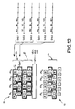
- the figure 12 illustrates an exemplary addressing of a Delta type screen, partially shown, by means of a device according to the invention.
- Each pixel is constituted by the combination of three sub-pixels Rk, Vk and Bk.
- the signals SIG1, SIG2, SIG3 represent the samples of the luminance signals sent respectively to the subpixels Rk, Vk and Rk, situated on the same video column.
- the sub-pixels of the physical line Li respectively receive three sequences SIG1, SIG2, SIG3 respectively comprising the samples R1, R3, R5, ..., V1, V3, V5, ..., and B2, B4, B6, ...
- the sub-pixels of the physical line Li + 1 respectively receive three sequences SIG1, SIG2, SIG3 respectively comprising the samples R2, R4, R6, ..., V2, V4, V6, ..., and B3, B5, B7.
- the figure 14 illustrates the phase during which the writing of the data relating to the sub-pixels R, V and B of a video line LV is performed, and secondly, the reading of the data relating to the sub-pixels. pixels R, V and B of the previous video line LV-1, then the next phase, during which is performed, on the one hand, the writing of the data relating to the sub-pixels R, G and B of a line LV + 1 video, and secondly, reading the data relating to the sub-pixels R, G and B of the video line LV written during the previous phase.
- the writing of said video line LV and the reading of said video line LV-1 are done simultaneously and are synchronized by the first synchronization means 76 which sends to the write control means 72 and the means 74, a signal W / R, shown in FIG. figure 14 , allowing, on the one hand, to progressively write the video data relating to the sub-pixels R, G or B, and on the other hand, to read said data corresponding to the respective spatial positions of each of the sub-pixels R , V and B on the screen.
- the write phase of the LV line is illustrated by the lines RSTW, WAB, WDA, and W / R while the reading phase of the line LV-1 is illustrated by the lines RSTR, RVAB, RVRDA, BDA, BRDA .
- the line RSTW represents an initialization signal of the write phase
- the line WAB represents the successive addresses in the memories 80, 82, 84 in which the digital data representing the samples Rk, Vk and Bk will be stored successively.
- the line WDA represents said digital data transported respectively by data buses 86, 88, 90.
- the line W / R represents the synchronization signal of the successive write and read phases sent by the first synchronization means 76.
- RSTR represents a signal initialization of the reading phase.
- the line RVAB represents the successive addresses in the memories 80, 82 and 84 in which are already stored the digital data representing the samples Rk, Vk.
- the line RVRDA represents the data Rk, Vk read respectively on data buses 94 and 96.
- the line BAB represents the successive addresses in the memories 80, 82 and 84 in which are already stored the digital data representing the samples Bk, the line BRDA the Bk data read on bus 92.
- the data Rk, Vk and Bk represented on the line WDA are written progressively, while the data RVRDA and BRDA, previously written, are read correlatively to their respective positions on the surface of the screen.
- the figure 1 5 partially illustrates a stack 202 and a stack 210 and the figure 16 illustrates the phase during which, on the one hand, the writing of the data relating to the subpixels R, G and B of a video line LV, and on the other hand, the phase during which the reading data relating to the sub-pixels R, G and B of said video line LV previously written in the cells 202 and 210, then the phase, during which is performed, on the one hand, the writing of the data relating to the sub -pixels R, V and B of the video line LV + 1, and secondly, the phase during which the data relating to the sub-pixels R, G and B of said video line LV + 1 are read, previously written in the cells 202 and 210.
- the synchronization of said write and read phases is performed by means of a second synchronization means 240 providing, on the one hand, to the demultiplexing stage 220 a first signal OW period of frequency F controlling the writing of the video data relating to the sub-pixels R, V and B situated on an odd video column respectively in the cells 202, 204 and 206, and a second periodic signal EW of frequency F controlling the writing of the video data relating to the subpixels R, G and B located on a video column pair respectively in the piles 212, 214 and 216, and on the other hand, at the multiplexing stage 230 a third periodic signal RD of frequency 2 * F controlling the reading of the video data relating to the sub-pixels of an even (odd) video column selected by the multiplexing stage 230.
- a third periodic signal RD of frequency 2 * F controlling the reading of the video data relating to the sub-pixels of an even (odd) video column selected by the multiplexing stage 230.
- the line IE represents an initialization signal of the write phase
- the line OW represents the control signal of the writing of the video data relating to the subpixels R, G and B located on an odd video column
- the EW line represents the control signal of the writing of the video data relating to the subpixels R, G and B located on an even video column
- the line WDA represents the digital data to be written in the cells 202 and 210
- the line IL represents an initialization signal of the read phase
- the line RDA represents the data read
- the line OEE represents a selection signal of the data relating to the subpixels R, V and B located on an odd video column
- the line EOE represents a signal for selecting the data relating to the subpixels R, V and B situated on an even video column.
- the writing in the stack 202 of the video data relating to the sub-pixels R, G and B located on an odd video column is synchronized on each rising edge of the signal OW.
- the writing, in the stack 210, of the video data relating to the subpixels R, V and B situated on an even video column is synchronized on each rising edge of the signal EW.
- the RD signal for reading the digital data has a frequency twice that of the OW and EW signals.
- the read phases start when the batteries 202 and 212 are half full. So in the example of the figure 16 , the odd data are read at each rising edge of the signal RD from a time coinciding with the writing, of the 321 nth data, located in this example at half of the stack 202, and when the OEE signal has a logic level High.
- the even data are read at each rising edge of the signal RD at a time coinciding with the writing, in the stack 212, of the 321 nd data when the signal EOE has a high logic level.
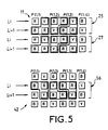
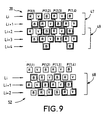
- the Figures 4 to 9 illustrate a combination of sub-pixels in which two physical lines Li and Li + 1 are used to form a video line of the image to be displayed, and said image is decomposed into an odd field 9, 11, 13, 15, 17, 19 and 20 comprising odd video lines 21, 23, 25, 27, 29, 31, 33, 35, 37, 39, 41, 43, 45, 47 and 49, and an even frame 40, 42, 44, 46, 48, 50 and 52 comprising paired video lines 54, 56, 58, 60, 62, 64, 65, 66, 67 and 68, said odd and even fields being shifted, relative to one another, physical line, so as to allow interleaving of the odd video lines with the even video lines.
- the physical lines Li used to constitute the video lines 54, 56, 58, 64, 65 and 67 are also used to constitute the physical lines Li + 1 of the odd video lines 21, 25, 29, 35, 39 and 43 respectively. This allows interleaving of said even video lines and said odd video lines.
- the multiplexing stage 220 selects the digital signal sequences relating to two contiguous sub-pixels located on the physical line Li (respectively Li + 1) and to a sub-pixel located on the physical line Li + 1 (respectively Li) , then the digital signal sequences relating to a sub-pixel located on the line Li (respectively Li + 1) and two sub-pixels located on the line Li + 1 (respectively Li) to address pixel of a video line of the image to display.
- the multiplexing stage 220 selects the digital signal sequences relating to a first sub-pixel located on the physical line Li and the digital signal sequences relating to a second sub-pixel adjacent to the first sub-pixel, and located on the physical line Li + 1 to address a pixel of the video line 43 and 45 (respectively 67).
- This combination mode is particularly suitable for uses that do not require a good colorimetry but rather require a good fineness of detail, insofar as on the one hand, it makes it possible to triple the horizontal resolution with respect to the modes of combination of the prior art described above, and secondly, it causes spectrum folds known as English colored aliasing producing an iridescence of the details of the displayed image.
- the sampling of the video signals sent to the combined sub-pixels is carried out either simultaneously or in spatial mode, that is to say at different times corresponding to the respective positions of said sub-pixels on the surface of the screen.
- the resolution is improved, regardless of the type of screen addressed.
- the resolution is equal to M * 2/3 and therefore twice the resolution obtained by the addressing modes of these screens by devices of the prior art and the vertical resolution is equal to at N / 2 for strictly vertical lines and at N for diagonal lines.
Landscapes
- Engineering & Computer Science (AREA)
- Physics & Mathematics (AREA)
- Computer Hardware Design (AREA)
- General Physics & Mathematics (AREA)
- Theoretical Computer Science (AREA)
- Control Of Indicators Other Than Cathode Ray Tubes (AREA)
- Liquid Crystal Display Device Control (AREA)
- Control Of Gas Discharge Display Tubes (AREA)
Claims (6)
- Vorrichtung zum Adressieren eines Matrixbildschirms, der geeignet ist, Bilder zu zeigen, mit einer Vielzahl von Videozeilen und -spalten, deren bildende Pixel sich aus einer Kombination aus einer Vielzahl von Subpixeln ergeben, die den Primärfarben (R, V und B) entsprechen, die jeweils ein Luminanz-Videosignal empfangen und die gemäß einem Gitter mit N physikalischen Zeilen und M physikalischen Spalten verteilt sind, wobei die Vorrichtung zwischen einer Demultiplexstufe (220) und einer Multiplexstufe (230) mindestens eine Speicherstufe (70, 198) aufweist, dadurch gekennzeichnet, dass die Speicherstufe (70, 198) geeignet ist, um über die Demultiplexstufe (220) eine Vielzahl von Sequenzen digitaler Daten, die jeweils ein Luminanz-Videosignal darstellen, das zuvor digitalisiert wurde, zu empfangen und zu speichern, und um die Luminanz-Videosignale an die Multiplexstufe (230) abzugeben, wobei Letztere geeignet ist, um eine Sequenz digitaler Daten auszuwählen, die einer gegebenen Kombination von Subpixeln des anzuzeigenden Bildes entspricht, wobei in Abhängigkeit von der gegebenen Kombination die zuvor in der Speicherstufe (70, 198) gespeicherten digitalen Daten verwendet werden.
- Vorrichtung nach Anspruch 1, bei der die Speicherstufe (198) zwei parallele Zweige aufweist - einen ersten Zweig, in dem ein erster Block (200) mit mindestens drei FIFO-Stacks, nämlich einem ersten Stack (202), einem zweiten Stack (204) und einem dritten Stack (206) angeordnet ist, die jeweils dazu bestimmt sind, die Videodaten zu den Subpixeln zu enthalten, die den Primärfarben (R, V und B) entsprechen und sich auf einer der physikalischen Zeilen, die eine gerade Videozeile bildet, befinden, und einen zweiten Zweig, in dem ein zweiter Block (200) mit ebenfalls mindestens drei FIFO-Stacks, nämlich einem vierten Stack (212), einem fünften Stack (214) und einem sechsten Stack (216) angeordnet ist, die jeweils dazu bestimmt sind, die Videodaten zu den Subpixeln zu enthalten, die den Primärfarben (R, V und B) entsprechen und sich auf einer der physikalischen Zeilen, die eine ungerade Videozeile bildet, befinden.
- Vorrichtung nach Anspruch 1, ferner mit einem Mittel (72), um das Schreiben der digitalen Daten in Speicher (80, 82, 84) der Speicherstufe zu steuern und einem Mittel (74), um das Lesen der Daten aus den Speichern (80, 82, 84) zu steuern, wobei die Schreibsteuermittel (72) und Lesesteuermittel (74) mit einem ersten Mittel (76) zur Synchronisierung der Schreib- und Lesephasen verbunden sind.
- Vorrichtung nach Anspruch 3, bei der jeder der Speicher (80, 82 und 84) zwei einzelne Bereiche aufweist - einen ersten Bereich (102), in dem die digitalen Daten zu den Subpixeln, die den Primärfarben (R, V und B) einer gegebenen Videozeile entsprechen, während einer gegebenen Schreibphase geschrieben werden, und einen zweiten Bereich (104), aus dem während der Schreibphase die digitalen Daten zu den Subpixeln, die den Primärfarben (R, V und B) einer während der vorigen Schreibphase geschriebenen Videozeile entsprechen, gelesen werden.
- Vorrichtung nach Anspruch 2, bei der die Demultiplexstufe (220) geeignet ist um abzuzweigen: zum einen die Daten zu den Subpixeln, die den Primärfarben (R, V und B) der ungeraden Videospalten entsprechen, zu dem ersten Block (200), so dass die Daten während einer Schreibphase einer Videozeile mit einer Dauer D in den ersten Stack (202) beziehungsweise in den zweiten Stack (204) beziehungsweise in den dritten Stack (206) geschrieben werden, und zum anderen die Daten zu den Subpixeln, die den Primärfarben (R, V und B) der geraden Videospalten entsprechen, zu dem zweiten Block (210) abzuzweigen, so dass die Daten während der Schreibphase in den vierten Stack (212) beziehungsweise in den fünften Stack (214) beziehungsweise in den sechsten Stack (216) geschrieben werden.
- Vorrichtung nach Anspruch 2 oder nach Anspruch 5, ferner mit einem Synchronisationsmittel (240), das einerseits mit der Demultiplexstufe (220) verbunden ist und dieser Stufe (220) ein erstes periodisches Signal OW mit einer Frequenz F, das das Schreiben der Videodaten zu den Subpixeln, die den Primärfarben (R, V und B) entsprechen und sich in einer ungeraden Videospalte befinden, in den ersten Stack (202) beziehungsweise in den zweiten Stack (204) beziehungsweise in den dritten Stack (206) steuert, und ein zweites periodisches Signal EW mit einer Frequenz F, das das Schreiben der Videodaten zu den Subpixeln, die den Primärfarben (R, V und B) entsprechen und sich in einer geraden Videospalte befinden, in den vierten Stack (212) beziehungsweise in den fünften Stack (214) beziehungsweise in den sechsten Stack (216) steuert, abgibt, wobei dieses Synchronisationsmittel (240) andererseits mit der Multiplexstufe (230) verbunden ist und dieser Stufe (230) ein drittes periodisches Signal RD mit einer Frequenz 2*F abgibt, das das Lesen der Videodaten zu den Subpixeln einer geraden beziehungsweise ungeraden Videozeile, die durch die Multiplexstufe (230) ausgewählt wird, steuert.
Applications Claiming Priority (3)
| Application Number | Priority Date | Filing Date | Title |
|---|---|---|---|
| FR9515405A FR2742910B1 (fr) | 1995-12-22 | 1995-12-22 | Procede et dispositif d'adressage d'un ecran matriciel |
| FR9515405 | 1995-12-22 | ||
| PCT/FR1996/002013 WO1997023861A1 (fr) | 1995-12-22 | 1996-12-18 | Dispositif d'adressage d'un ecran matriciel |
Publications (2)
| Publication Number | Publication Date |
|---|---|
| EP0976122A1 EP0976122A1 (de) | 2000-02-02 |
| EP0976122B1 true EP0976122B1 (de) | 2009-03-04 |
Family
ID=9485892
Family Applications (1)
| Application Number | Title | Priority Date | Filing Date |
|---|---|---|---|
| EP96942417A Expired - Lifetime EP0976122B1 (de) | 1995-12-22 | 1996-12-18 | Matrixanzeigeadressierungsverfahren |
Country Status (7)
| Country | Link |
|---|---|
| US (1) | US6252613B1 (de) |
| EP (1) | EP0976122B1 (de) |
| JP (1) | JP4105228B2 (de) |
| KR (1) | KR100425248B1 (de) |
| DE (1) | DE69637857D1 (de) |
| FR (1) | FR2742910B1 (de) |
| WO (1) | WO1997023861A1 (de) |
Families Citing this family (18)
| Publication number | Priority date | Publication date | Assignee | Title |
|---|---|---|---|---|
| US7286136B2 (en) | 1997-09-13 | 2007-10-23 | Vp Assets Limited | Display and weighted dot rendering method |
| DE19746329A1 (de) | 1997-09-13 | 1999-03-18 | Gia Chuong Dipl Ing Phan | Display und Verfahren zur Ansteuerung des Displays |
| DE19746576A1 (de) * | 1997-10-22 | 1999-04-29 | Zeiss Carl Fa | Verfahren für die Bilderzeugung auf einem Farbbildschirm und ein dazu geeigneter Farbbildschirm |
| JP4158874B2 (ja) | 2000-04-07 | 2008-10-01 | 株式会社日立プラズマパテントライセンシング | 画像表示方法および表示装置 |
| US7027013B2 (en) | 2000-12-22 | 2006-04-11 | Ifire Technology, Inc. | Shared pixel electroluminescent display driver system |
| US6720972B2 (en) | 2001-02-28 | 2004-04-13 | Honeywell International Inc. | Method and apparatus for remapping subpixels for a color display |
| JP2003043990A (ja) * | 2001-07-31 | 2003-02-14 | Fujitsu Ltd | カラー画像表示方法 |
| KR100489445B1 (ko) | 2001-11-29 | 2005-05-17 | 엘지전자 주식회사 | 플라즈마 표시 패널의 구동방법 |
| JP2005351920A (ja) * | 2004-06-08 | 2005-12-22 | Semiconductor Energy Lab Co Ltd | 表示装置の制御回路及びそれを内蔵した表示装置・電子機器並びにその駆動方法 |
| US7705821B2 (en) * | 2005-01-31 | 2010-04-27 | Semiconductor Energy Laboratory Co., Ltd. | Driving method using divided frame period |
| WO2008047725A1 (en) * | 2006-10-13 | 2008-04-24 | Sharp Kabushiki Kaisha | Display device, and signal converting device |
| JP5441312B2 (ja) * | 2007-02-09 | 2014-03-12 | 株式会社ジャパンディスプレイ | 表示装置 |
| TWI395195B (zh) * | 2008-07-30 | 2013-05-01 | Orise Technology Co Ltd | 共用同一遞色演算表的方法及使用其之顯示面板驅動方法 |
| WO2012067038A1 (ja) * | 2010-11-15 | 2012-05-24 | シャープ株式会社 | 多原色表示装置 |
| CN102903318B (zh) * | 2011-07-29 | 2015-07-08 | 深圳云英谷科技有限公司 | 显示器的子像素排列及其呈现方法 |
| KR102825728B1 (ko) * | 2016-11-30 | 2025-06-26 | 엘지디스플레이 주식회사 | 유기 발광 다이오드 표시 장치 |
| US20180168855A1 (en) * | 2016-12-15 | 2018-06-21 | Penguin Fingers, Llc | Joint compress cold pack |
| EP3678182A4 (de) | 2017-08-31 | 2020-09-02 | Kunshan Go-Visionox Opto-Electronics Co., Ltd. | Pixelstruktur, oled-anzeigevorrichtung und ansteuerungsverfahren |
Family Cites Families (11)
| Publication number | Priority date | Publication date | Assignee | Title |
|---|---|---|---|---|
| DE3634092A1 (de) * | 1986-10-07 | 1988-04-14 | Thomson Brandt Gmbh | Schaltungsanordnung zur verzoegerung eines digitalen signals |
| ATE49075T1 (de) * | 1987-01-08 | 1990-01-15 | Hosiden Electronics Co | Flaches anzeigegeraet. |
| US4792856A (en) * | 1987-04-14 | 1988-12-20 | Rca Licensing Corporation | Sampled data memory system as for a television picture magnification system |
| JP2702941B2 (ja) * | 1987-10-28 | 1998-01-26 | 株式会社日立製作所 | 液晶表示装置 |
| JPH0248863A (ja) * | 1988-08-10 | 1990-02-19 | Nec Corp | ディジタルビデオ信号処理回路 |
| DE68923683T2 (de) * | 1988-11-05 | 1996-02-15 | Sharp Kk | Steuereinrichtung und -verfahren für eine Flüssigkristallanzeigetafel. |
| US5841480A (en) * | 1989-09-07 | 1998-11-24 | Advanced Television Technology Center | Film to video format converter using least significant look-up table |
| EP0428324A2 (de) * | 1989-11-13 | 1991-05-22 | DELCO ELECTRONICS CORPORATION (a Delaware corp.) | Matrixadressiertes flaches Anzeigegerät und CRT kompatible Steuerschaltung |
| JPH06332843A (ja) * | 1992-06-24 | 1994-12-02 | Seiko Epson Corp | 動画映像データ転送装置およびコンピュータシステム |
| FR2703814B1 (fr) * | 1993-04-08 | 1995-07-07 | Sagem | Afficheur matriciel en couleurs. |
| JP3219640B2 (ja) * | 1994-06-06 | 2001-10-15 | キヤノン株式会社 | ディスプレイ装置 |
-
1995
- 1995-12-22 FR FR9515405A patent/FR2742910B1/fr not_active Expired - Fee Related
-
1996
- 1996-12-18 JP JP52335497A patent/JP4105228B2/ja not_active Expired - Fee Related
- 1996-12-18 KR KR10-1998-0704070A patent/KR100425248B1/ko not_active Expired - Fee Related
- 1996-12-18 DE DE69637857T patent/DE69637857D1/de not_active Expired - Lifetime
- 1996-12-18 WO PCT/FR1996/002013 patent/WO1997023861A1/fr not_active Ceased
- 1996-12-18 EP EP96942417A patent/EP0976122B1/de not_active Expired - Lifetime
- 1996-12-18 US US09/077,379 patent/US6252613B1/en not_active Expired - Lifetime
Also Published As
| Publication number | Publication date |
|---|---|
| KR100425248B1 (ko) | 2004-07-27 |
| JP2000502813A (ja) | 2000-03-07 |
| US6252613B1 (en) | 2001-06-26 |
| KR19990071791A (ko) | 1999-09-27 |
| JP4105228B2 (ja) | 2008-06-25 |
| EP0976122A1 (de) | 2000-02-02 |
| WO1997023861A1 (fr) | 1997-07-03 |
| FR2742910B1 (fr) | 1998-04-17 |
| FR2742910A1 (fr) | 1997-06-27 |
| DE69637857D1 (de) | 2009-04-16 |
Similar Documents
| Publication | Publication Date | Title |
|---|---|---|
| EP0976122A1 (de) | Matrixanzeigeadressierungsverfahren | |
| EP0311500B1 (de) | Halbton-Anzeigeverfahren für einen Matrix-Bildschirm | |
| EP0697161B1 (de) | Autosterioskopisches videosystem und vorrichtung | |
| CH618283A5 (de) | ||
| FR2599873A1 (fr) | Systeme d'affichage video | |
| FR2703814A1 (fr) | Afficheur matriciel en couleurs. | |
| EP3079142B1 (de) | Bildanzeigeverfahren auf matrix-bildschirm | |
| FR2554948A1 (fr) | Procedes et appareils de codage et d'affectation d'emplacements de memoire pour affichage d'images traitees numeriquement | |
| EP0379810A2 (de) | Methode der Darstellung von Grauwerten auf einem Matrix-Bildschirm | |
| FR2543776A1 (fr) | Agencement de correction de distorsion de la trame dans un systeme de traitement video numerique | |
| EP0306403B1 (de) | Flachbildschirmanzeigevorrichtung mit vom Benutzer gesteuerter Anzeige | |
| EP0524842B1 (de) | Vorrichtung zur Fernsehbildwiedergabe in Echtzeit auf einem Anzeigebildschirm | |
| EP0602218A1 (de) | Fluessigkristall-anzeige mit aktiver matrix | |
| FR2776107A1 (fr) | Procede d'affichage de donnees sur un afficheur matriciel | |
| EP0472463B1 (de) | Verfahren zur Darstellung von Bildern auf einem Matrixbildschirm sowie System zur Durchführung dieses Verfahrens | |
| FR2551286A1 (fr) | Dispositif de visualisation d'une image de television couleur balayee progressivement | |
| EP0432072B1 (de) | Bildverarbeitungsverfahren und -system | |
| FR2803076A1 (fr) | Procede d'adressage de panneau d'affichage au plasma | |
| FR2660471A1 (fr) | Dispositif de visualisation de securite utilisant un ecran a matrice de points et tableau de bord d'aeronef comportant au moins un tel dispositif. | |
| EP2983167B1 (de) | Lcd-anzeigegerät mit zeilenadressierung durch stichprobenerfassung und umwandlung, sowie anzeigeverfahren | |
| FR2667211A1 (fr) | Systeme de thermographie infrarouge pour la realisation d'une loupe numerique plein ecran avec une camera utilisant le balayage serie-parallele. | |
| EP0047692B1 (de) | Verfahren zum Erzeugen von Steuersignalen für eine Plasmaanzeigeeinrichtung und von nach diesem Verfahren erzeugten Signalen gesteuerte Plasmaanzeigeeinrichtung | |
| FR2836588A1 (fr) | Procede d'affichage numerique d'image et dispositif d'affichage numerique | |
| EP1131810A1 (de) | Addressierverfahren und plasmaanzeigepaneel basiert auf separaten gerade und ungerade numerierten linienaddressen | |
| EP0506530A1 (de) | Matrixanzeige mit verbesserter Auflösung und Adressierungsverfahren einer solchen Anzeige |
Legal Events
| Date | Code | Title | Description |
|---|---|---|---|
| PUAI | Public reference made under article 153(3) epc to a published international application that has entered the european phase |
Free format text: ORIGINAL CODE: 0009012 |
|
| 17P | Request for examination filed |
Effective date: 19980318 |
|
| AK | Designated contracting states |
Kind code of ref document: A1 Designated state(s): DE FR GB |
|
| 17Q | First examination report despatched |
Effective date: 20070503 |
|
| GRAP | Despatch of communication of intention to grant a patent |
Free format text: ORIGINAL CODE: EPIDOSNIGR1 |
|
| GRAS | Grant fee paid |
Free format text: ORIGINAL CODE: EPIDOSNIGR3 |
|
| GRAA | (expected) grant |
Free format text: ORIGINAL CODE: 0009210 |
|
| AK | Designated contracting states |
Kind code of ref document: B1 Designated state(s): DE FR GB |
|
| REG | Reference to a national code |
Ref country code: GB Ref legal event code: FG4D Free format text: NOT ENGLISH |
|
| REF | Corresponds to: |
Ref document number: 69637857 Country of ref document: DE Date of ref document: 20090416 Kind code of ref document: P |
|
| PLBE | No opposition filed within time limit |
Free format text: ORIGINAL CODE: 0009261 |
|
| STAA | Information on the status of an ep patent application or granted ep patent |
Free format text: STATUS: NO OPPOSITION FILED WITHIN TIME LIMIT |
|
| 26N | No opposition filed |
Effective date: 20091207 |
|
| PGFP | Annual fee paid to national office [announced via postgrant information from national office to epo] |
Ref country code: DE Payment date: 20141219 Year of fee payment: 19 |
|
| PGFP | Annual fee paid to national office [announced via postgrant information from national office to epo] |
Ref country code: FR Payment date: 20141215 Year of fee payment: 19 Ref country code: GB Payment date: 20150105 Year of fee payment: 19 |
|
| REG | Reference to a national code |
Ref country code: DE Ref legal event code: R119 Ref document number: 69637857 Country of ref document: DE |
|
| GBPC | Gb: european patent ceased through non-payment of renewal fee |
Effective date: 20151218 |
|
| REG | Reference to a national code |
Ref country code: FR Ref legal event code: ST Effective date: 20160831 |
|
| PG25 | Lapsed in a contracting state [announced via postgrant information from national office to epo] |
Ref country code: DE Free format text: LAPSE BECAUSE OF NON-PAYMENT OF DUE FEES Effective date: 20160701 Ref country code: GB Free format text: LAPSE BECAUSE OF NON-PAYMENT OF DUE FEES Effective date: 20151218 |
|
| PG25 | Lapsed in a contracting state [announced via postgrant information from national office to epo] |
Ref country code: FR Free format text: LAPSE BECAUSE OF NON-PAYMENT OF DUE FEES Effective date: 20151231 |