EP0976252B1 - Videoendstufe mit selbstregelnder strahlstrombegrenzung - Google Patents
Videoendstufe mit selbstregelnder strahlstrombegrenzung Download PDFInfo
- Publication number
- EP0976252B1 EP0976252B1 EP97951657A EP97951657A EP0976252B1 EP 0976252 B1 EP0976252 B1 EP 0976252B1 EP 97951657 A EP97951657 A EP 97951657A EP 97951657 A EP97951657 A EP 97951657A EP 0976252 B1 EP0976252 B1 EP 0976252B1
- Authority
- EP
- European Patent Office
- Prior art keywords
- signal
- output
- video
- coupled
- transistor
- Prior art date
- Legal status (The legal status is an assumption and is not a legal conclusion. Google has not performed a legal analysis and makes no representation as to the accuracy of the status listed.)
- Expired - Lifetime
Links
- 238000012545 processing Methods 0.000 claims description 25
- 238000012937 correction Methods 0.000 description 5
- 238000010586 diagram Methods 0.000 description 4
- 238000013459 approach Methods 0.000 description 3
- 229920006395 saturated elastomer Polymers 0.000 description 3
- 238000005094 computer simulation Methods 0.000 description 2
- 230000000694 effects Effects 0.000 description 2
- OAICVXFJPJFONN-UHFFFAOYSA-N Phosphorus Chemical compound [P] OAICVXFJPJFONN-UHFFFAOYSA-N 0.000 description 1
- 230000002411 adverse Effects 0.000 description 1
- 230000032683 aging Effects 0.000 description 1
- 230000003679 aging effect Effects 0.000 description 1
- 239000003990 capacitor Substances 0.000 description 1
- 230000015556 catabolic process Effects 0.000 description 1
- 239000004020 conductor Substances 0.000 description 1
- 230000008878 coupling Effects 0.000 description 1
- 238000010168 coupling process Methods 0.000 description 1
- 238000005859 coupling reaction Methods 0.000 description 1
- 238000006731 degradation reaction Methods 0.000 description 1
- 238000010894 electron beam technology Methods 0.000 description 1
- 230000001747 exhibiting effect Effects 0.000 description 1
- 238000001914 filtration Methods 0.000 description 1
- 244000145841 kine Species 0.000 description 1
- 238000005259 measurement Methods 0.000 description 1
- 238000012986 modification Methods 0.000 description 1
- 230000004048 modification Effects 0.000 description 1
- 238000012544 monitoring process Methods 0.000 description 1
- 238000011084 recovery Methods 0.000 description 1
- 230000011664 signaling Effects 0.000 description 1
- 230000002277 temperature effect Effects 0.000 description 1
Images



Classifications
-
- H—ELECTRICITY
- H04—ELECTRIC COMMUNICATION TECHNIQUE
- H04N—PICTORIAL COMMUNICATION, e.g. TELEVISION
- H04N9/00—Details of colour television systems
- H04N9/64—Circuits for processing colour signals
- H04N9/645—Beam current control means
-
- H—ELECTRICITY
- H04—ELECTRIC COMMUNICATION TECHNIQUE
- H04N—PICTORIAL COMMUNICATION, e.g. TELEVISION
- H04N5/00—Details of television systems
- H04N5/44—Receiver circuitry for the reception of television signals according to analogue transmission standards
- H04N5/57—Control of contrast or brightness
- H04N5/59—Control of contrast or brightness in dependence upon beam current of cathode ray tube
Definitions
- This invention relates to a video processing system including a video output amplifier for providing video drive signals to an image display device such as a kinescope.
- this invention concerns a video output driver amplifier which can automatically self-regulate the peak beam current output provided to a display.
- video output amplifiers are used to provide amplified video signals to intensity control electrodes (e.g., cathodes) of a display device (e.g., kinescope).
- the amplified video signals are provided in the form of, for example, R, G, and B beam currents to the respective cathode of an image display device.
- One reason is that if an excessive output beam current is developed in response to a large amplitude video signal representative of highly saturated color image information or peak white image information at the input of the video amplifiers, the output transistors of the amplifiers may saturate in response thereof.
- a saturated output amplifier can produce an objectionable white or colored image smear following a displayed image area produced by a large amplitude video drive signal. For example, if a white image area is displayed and the biasing of the red video output transistor is such that the red output transistor saturates, a red color smear following the white image is likely to be produced as a result of the red video output transistor exhibiting a saturated conductive state together with the slow "recovery time" of the red output transistor due to transistor charge storage effects.
- excessive beam current may also cause degradation of the performance of the receiver's deflection system, electron beam spot defocusing and picture blooming. Such a high beam current may also exceed the safe operating capability of the kinescope, possibly causing damage to the kinescope and associated circuit components.
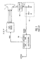
- FIG. 1 One common approach to limiting beam current to a CRT is shown in FIG. 1. This approach involves monitoring the average beam current at the high voltage supply of a CRT 101 and providing a control signal representative of the magnitude of the average beam current.
- the average beam current is derived from a filtering capacitor C1. If the average beam current exceeds a predetermined threshold, then the parameters of the contrast and brightness adjustment stages 104A and 104B in the video processing circuit 104 are changed in accordance to the control signal.
- the beam current at the output of the video driver amplifier (20', 22', 24') is also reduced. The beam current is therefore controlled via the contrast and brightness processing stages of the video processing system, long before the video signal reaches the video driver stage.
- EP 0 680 226 A2 discloses a kinescope driver apparatus having a gamma correction feature.
- Gamma correction is desirable to compensate for the non-linear relationship between the input signal and the light output of a picture tube.
- the apparatus comprises buffer amplifier 70 coupled to cathode K1 via resistor 79, which senses the cathode current.
- Buffer amplifier 70 is coupled to linear amplifier 60 via network 80.
- the feedback signal provided by network 80 provides gamma correction as shown in Fig. 1.
- the apparatus does not provide a peak beam limiting feature which limits the output to the cathode to a predetermined level when the cathode current exceeds a predetermined peak cathode current level.
- U.S. Pat. No. 4,599,642 discloses a video signal processor that selectively couples a beam current control signal to a luminance processor and a chrominance processor during white level drive control intervals and black level bias control intervals.
- the processor includes a beam limiter control circuit that receives a summed signal representative of a combination of cathode currents and provides a control signal to the luminance and chrominance processors.
- the apparatus uses a combined cathode current signal to generate the control signal and provides the control signal to various processors, rather than to a particular drive amplifier associated with a selected cathode.
- the present inventor recognizes that, however, it is important to monitor and control not only the average beam current but also the peak beam current. Excessive average beam current and peak beam current can cause different problems mentioned above.
- An average beam current limiter is needed particularly to protect the high voltage supply system from excessive power drain, and the display from excessive power dissipation. Excessive average beam current may also result in shadow mask beam location error, therefore causing color error, in direct view tubes with a shadow mask.
- a peak beam current limiter is needed to prevent excessive instantaneous beam current that may cause excessive aging of the phosphor screen and poor spot size. Poor or large spot size is equivalent to poor focus and loss of resolution.
- a video signal processing system including an image reproducing device for displaying video information in response to a video signal applied thereto.
- the processing system includes an apparatus comprising a video output driver stage with a video signal input and a video signal output for providing an amplified video signal.
- the apparatus is characterized in that the video output driver stage comprises means for amplifying the input video signal and coupling said output signal to the image reproducing device.
- the output driver also includes a sensing output for providing thereat a sensed signal representative of current conducted by the image reproducing display device.
- the video driver stage further comprises measurement and control means for sensing the sensed signal and for providing a feedback signal to an input component of said video output driver stage for limiting the peak beam current conducted by said image reproducing display device to a predetermined value.
- FIG. 2 is an example of a block diagram of a video processing system according to the principles of the present invention.
- the video processing system includes a typical video processing subsystem 204 comprising luminance and chromanance processing sections for processing an input video signal.
- the video processing system also employs a known average beam current limiting system including an average beam current sensing and feedback circuit 103 as described above, and as shown in FIG. 1.
- the video processing system further comprises video driver circuits 20, 22, and 24 for respective blue, green and red video signals.
- Each video driver circuit (e.g., 20) comprises an amplifier circuit 27 for amplifying the respective video signal, a sensing circuit 28 for measuring the AKB and the peak beam current, and a control circuit 29 for comparing the peak beam current to a predetermined threshold and for limiting the peak beam current to the threshold.
- the beam current sensed by the sensing circuit 28 is also provided to an AKB processing system 30.
- the AKB processing system 30 is a known system for automatically establishing the proper black image representative current levels for each electron gun of a kinescope. As a result of this operation, the reproduced picture is prevented from being adversely affected by variations of kinescope bias from a desired level (e.g., due to aging and temperature effects).
- An AKB system typically operates during image retrace blanking intervals, at which time the kinescope conducts a small black level representative blanking current. This current is monitored by the AKB system 30 to generate a correction voltage representing the difference between the sensed black current level and a desired black current level. The correction voltage is applied to video signal processing circuits 204 preceding the kinescope with a sense for reducing the difference.
- AKB systems are disclosed, for example, in U.S. Pat. Nos. 4,263,622, and 4,277,798, both issued to Werner Hinn.
- the video driver output stage 20, as shown in FIG. 2 in block diagram form will now be described in detail, with exemplary circuit components shown in FIG. 3.
- FIG 3 shows a source of color image representative video signals 10 providing low level color signals blue (b), green (g) and red (r), to respective b, g, and r color signal driver amplifier stages 20, 22 and 24 of similar configuration.
- the source of color signals 10, for example, may be from the video processing stage 204 of a television as shown in FIG. 2.
- blue (b) color signal driver amplifier 20 also applies to red and green signal driver stages 22 and 24.
- High level output color video signals R, G. B from drivers 20, 22, and 24 are coupled via respective flash-over protection resistors R1, R2 and R3 of a color image reproducing kinescope 1.
- the flash-over protection resistors protect the drive circuitry from the harm of a kine arc occurring.
- a kinescope control grid 2 is biased by a high voltage source (not shown in FIG. 3), in common with respect to each of the cathode electrodes and forms a plurality of kinescope electron guns therewith.
- Blue driver 20 comprises an input component, Q101, which is a common emitter amplifier transistor arranged in a cascode driver amplifier configuration with an output common base amplifier transistor Q102.
- Input blue (b) color signal is coupled to the base input electrode of the transistor Q101.
- a bias of approximately 10 volts is applied to the base of transistor Q102.
- the output signal at the collector of Q102 serves as the input to a push-pull output stage comprising a NPN transistor Q106 and a PNP transistor Q107.
- Video output drive signal B is provided from both the emitter terminals of transistors Q106, and Q107, and is coupled to the blue cathode terminal of the kinescope as described above to provide drive current for the kinescope 1.
- the base conductor of a beam current measuring and controlling transistor Q108 is coupled to the collector terminal of Q107 through a base resistor R4.
- the collector of Q108 is connected to a bias voltage of approximately 10 V.
- the emitter of Q108 is fed back to the collector of lower cascode transistor Q101.
- a resistor R5 is connected to the collector terminal of the transistor Q107 to provide a sensed current to the AKB processing system 30, as discussed previously in connection with FIG. 2.
- IB 6 ma maximum
- This exemplary value is selected based on a rating of the kinescope for this particular implementation, so as to prevent the various problems due to high peak beam current as discussed above.
- Other threshold values may be selected according to other implementation requirements and the teaching of the present invention as discussed below.
- I B 2.065 ⁇ 10 ⁇ 6 ⁇ ( V cut-off + V G 1 ⁇ V cathode ) 2.97 ma
- Vcut-off and VGRID are also chosen based on the rating of the particular CRT used.
- Vcut-off is rated at 190 V (measured from cathode to grid), and VG1 is biased at 28 V.
- Vcathode 68 V when I B is at 6 ma .
- the circuit when V1 is below 3.54 V, the circuit will provide a beam current drive output which is non-clipped and is below the 6 ma threshold. That is, Q108 continuously monitors the potential at V4 which is in proportion to IB. Q108, however, will not conduct when V1 is below 3.54 volt and IB is less than 6 ma.
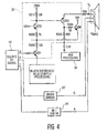
- FIG. 4 shows another embodiment of the present invention. This embodiment is similar to that shown in Fig. 3.
- the embodiment in FIG. 4 shows variations in component values to account for different bias voltages and ratings used in this embodiment.
- the operation of the embodiment shown in FIG. 4 is also similar to the above described operation of the embodiment in FIG. 3.
- the sensing and control transistor Q208 now has its emitter connected directly to the emitter of the upper cascode transistor Q202.
- the output stage of the video drive 20 now consists of only emitter follower transistor Q203 in stead of a push-pull pair as shown in FIG. 3.
- FIG. 5 shows the results of a computer simulation of the circuit depicted in FIG. 4.
- the graph shows that with the addition of the peak current sensing and limiting circuits 28 and 29 in the output driver 20, the peak beam current is limited to approximately 6 ma as desired, even with increasing signal input.
Landscapes
- Engineering & Computer Science (AREA)
- Multimedia (AREA)
- Signal Processing (AREA)
- Picture Signal Circuits (AREA)
- Transforming Electric Information Into Light Information (AREA)
- Television Receiver Circuits (AREA)
Claims (8)
- Vorrichtung zur Videosignalverarbeitung, die umfasst:einen Videosignaleingang (b), der mit einer Quelle von Videosignalen zum Empfang eines Videoeingangssignals verbunden ist;einen Videosignalausgang (B), der mit einer ausgewählten Kathode einer Vorrichtung zur Bildwiedergabe (1) verbunden ist, um ein Ausgangssignal zu liefern, und die ausgewählte Kathode einen hindurch fließenden Kathodenstrom als Reaktion auf das Ausgangssignal hat;Mittel (27), die zwischen dem Videosignaleingang und dem Videosignalausgang eingekoppelt sind, um das Videoeingangssignal zu verstärken und das Ausgangssignal zu bilden und die Mittel der Verstärkung einen Treiberverstärker (Q101) beinhalten;Mittel, die zur Messung des Kathodenstroms mit der Kathode verbunden sind, und die Mittel zur Messung ein erstes Signal (V4) liefern, das dem Kathodenstrom der ausgewählten Kathode entspricht;Mittel (Q108), die direkt zwischen die Messmittel und die Verstärkungsmittel eingekoppelt sind, um dem Treiberverstärker ein Rückkopplungssignal zu liefern und das Rückkopplungssignal nur dem ersten Signal entspricht, das Rückkopplungssignal den Ausgangwert des Treiberverstärkers auf eine vordefinierte Höhe begrenzt, dadurch das Eingangssignal auf eine vordefinierte Höhe begrenzt, wenn der Kathodenstrom einen vordefinierten Spitzenwert des Kathodenstroms übersteigt.
- Vorrichtung nach Anspruch 1, wobei das Mittel zur Rückkopplung einen bipolaren Transistor umfasst.
- Vorrichtung nach Anspruch 2, wobei der bipolare Transistor einen Basisanschluss beinhaltet, der mit dem Signalausgang verbunden ist, und einen Emitteranschluss, der mit der der Eingangskomponente verbunden ist.
- Vorrichtung nach Anspruch 1, wobei der Treiberverstärker einen normalen Emitterverstärker-Transistor umfasst.
- Vorrichtung nach Anspruch 4, wobei der Emitterverstärkertransistor in einer Konfiguration eines Kaskodentreiberverstärkers mit einem normalen Ausgangstransistor in Basisschaltung (Q102) verbunden ist.
- Vorrichtung nach Anspruch 5, wobei der Kaskodentreiberverstärker mit einer Gegentaktverstärkerstufe verbunden ist, die einen NPN- und einen PNP- Transistor umfasst, und die Gegentaktverstärkerstufe einen mit der Vorrichtung zur Bildwiedergabe verbundenen Ausgang hat.
- Vorrichtung nach Anspruch 6, wobei das Rüchkopplungsmittel mit dem Kollektor des PNP Transistors gekoppelt ist.
- Vorrichtung nach Anspruch 7, wobei der Kollektor des PNP Transistors an einen AKB-Verarbeitungsbaustein gekoppelt ist.
Applications Claiming Priority (3)
| Application Number | Priority Date | Filing Date | Title |
|---|---|---|---|
| GBGB9704536.3A GB9704536D0 (en) | 1997-03-05 | 1997-03-05 | CTC195 kine driver with peak beam current limiting |
| GB9704536 | 1997-03-05 | ||
| PCT/US1997/022843 WO1998039924A1 (en) | 1997-03-05 | 1997-12-15 | Video output stage with self-regulating beam current limiting |
Publications (2)
| Publication Number | Publication Date |
|---|---|
| EP0976252A1 EP0976252A1 (de) | 2000-02-02 |
| EP0976252B1 true EP0976252B1 (de) | 2006-05-03 |
Family
ID=10808727
Family Applications (1)
| Application Number | Title | Priority Date | Filing Date |
|---|---|---|---|
| EP97951657A Expired - Lifetime EP0976252B1 (de) | 1997-03-05 | 1997-12-15 | Videoendstufe mit selbstregelnder strahlstrombegrenzung |
Country Status (9)
| Country | Link |
|---|---|
| US (1) | US6614482B1 (de) |
| EP (1) | EP0976252B1 (de) |
| JP (1) | JP3804991B2 (de) |
| KR (1) | KR100505759B1 (de) |
| CN (1) | CN1214653C (de) |
| AU (1) | AU5523498A (de) |
| DE (1) | DE69735818T2 (de) |
| GB (1) | GB9704536D0 (de) |
| WO (1) | WO1998039924A1 (de) |
Families Citing this family (4)
| Publication number | Priority date | Publication date | Assignee | Title |
|---|---|---|---|---|
| SG94326A1 (en) * | 1999-06-19 | 2003-02-18 | Thomson Multimedia Sa | Television receiver comprising a cathode ray tube (crt) |
| US6897901B2 (en) * | 2001-03-14 | 2005-05-24 | Koninklijke Philips Electronics N.V. | Circuit for combining AKB and selective beam current limiting and projection television system utilizing same |
| EP1543679A1 (de) * | 2002-09-18 | 2005-06-22 | Koninklijke Philips Electronics N.V. | Strahlstrommessung |
| US7221227B2 (en) * | 2005-06-06 | 2007-05-22 | Avago Technologies Ecbu Ip (Singapore) Pte. Ltd. | Methods and apparatus for reducing output current oscillations of a driver provided with circuitry that senses and responds to excessive current draws of an output stage of the driver |
Family Cites Families (10)
| Publication number | Priority date | Publication date | Assignee | Title |
|---|---|---|---|---|
| US4207591A (en) * | 1978-02-09 | 1980-06-10 | Rca Corporation | Gated automatic beam current limiter in a video signal processing system |
| US4263622A (en) * | 1979-01-30 | 1981-04-21 | Rca Corporation | Automatic kinescope biasing system |
| US4277798A (en) * | 1979-04-18 | 1981-07-07 | Rca Corporation | Automatic kinescope biasing system with increased interference immunity |
| US4599642A (en) | 1984-03-02 | 1986-07-08 | Rca Corporation | Video signal processor with bias error compensation |
| US5134490A (en) * | 1989-04-18 | 1992-07-28 | Thomson Consumer Electronics, Inc. | Beam current limiter with brightness control threshold extension |
| US5313294A (en) * | 1990-03-20 | 1994-05-17 | Rca Thomson Licensing Corporation | Beam current limiting arrangement having a peak amplitude, responsive threshold |
| GB9124071D0 (en) | 1991-11-13 | 1992-01-02 | Thomson Consumer Electronics | Crt bias compensation |
| CA2145901C (en) * | 1994-04-28 | 2000-02-22 | Anton Werner Keller | Kinescope driver apparatus with gamma correction |
| US5488417A (en) | 1994-05-19 | 1996-01-30 | Thomson Consumer Electronics, Inc. | Automatic kinescope bias control system |
| US5714842A (en) * | 1995-07-21 | 1998-02-03 | Apple Computer, Inc. | Automatic cutoff control for a DC coupled CRT video drive |
-
1997
- 1997-03-05 GB GBGB9704536.3A patent/GB9704536D0/en active Pending
- 1997-12-15 DE DE69735818T patent/DE69735818T2/de not_active Expired - Fee Related
- 1997-12-15 JP JP53849798A patent/JP3804991B2/ja not_active Expired - Fee Related
- 1997-12-15 AU AU55234/98A patent/AU5523498A/en not_active Abandoned
- 1997-12-15 KR KR10-1999-7007944A patent/KR100505759B1/ko not_active Expired - Fee Related
- 1997-12-15 WO PCT/US1997/022843 patent/WO1998039924A1/en not_active Ceased
- 1997-12-15 US US09/380,445 patent/US6614482B1/en not_active Expired - Fee Related
- 1997-12-15 EP EP97951657A patent/EP0976252B1/de not_active Expired - Lifetime
- 1997-12-15 CN CNB971820007A patent/CN1214653C/zh not_active Expired - Fee Related
Also Published As
| Publication number | Publication date |
|---|---|
| GB9704536D0 (en) | 1997-04-23 |
| AU5523498A (en) | 1998-09-22 |
| JP3804991B2 (ja) | 2006-08-02 |
| CN1249109A (zh) | 2000-03-29 |
| JP2001512647A (ja) | 2001-08-21 |
| DE69735818T2 (de) | 2006-11-09 |
| US6614482B1 (en) | 2003-09-02 |
| EP0976252A1 (de) | 2000-02-02 |
| KR100505759B1 (ko) | 2005-08-04 |
| KR20000075865A (ko) | 2000-12-26 |
| CN1214653C (zh) | 2005-08-10 |
| WO1998039924A1 (en) | 1998-09-11 |
| DE69735818D1 (de) | 2006-06-08 |
Similar Documents
| Publication | Publication Date | Title |
|---|---|---|
| EP0414183B1 (de) | Dynamisches Videosystem einschliesslich automatischer Kontrast- und Weissausdehnungsverarbeitungsteile | |
| US4253121A (en) | Plural sequential operating mode automatic kinescope beam current limiter | |
| EP0414159B1 (de) | Verstärker zur Erzeugung einer steuerbaren nichtlinearen Transfercharakteristik zur Verbesserung eines Bildkontrasts | |
| JP2611755B2 (ja) | ビデオ信号処理装置における制御装置 | |
| EP0041554B1 (de) | Automatisches pegelregelungssystem für spitzenstrahlstron | |
| CA1228159A (en) | Video signal processor with automatic kinescope beam current limiter | |
| EP0976252B1 (de) | Videoendstufe mit selbstregelnder strahlstrombegrenzung | |
| US5313294A (en) | Beam current limiting arrangement having a peak amplitude, responsive threshold | |
| JPH04229771A (ja) | ビデオ表示装置 | |
| CA2114880C (en) | Black compensation circuit for a video display system | |
| US3647944A (en) | Kinescope bias arrangement to provide both constant amplitude dc restoration pulses and arc discharge protection | |
| US4365271A (en) | Television camera having a beam current control circuit | |
| JPS607871B2 (ja) | 信号処理回路 | |
| KR100345435B1 (ko) | 영상디스플레이장치및빔스캔속도변조회로 | |
| EP0551379B1 (de) | Anordnung zur Strahlstrombegrenzung mit einem von der Spitzenamplitude abhängigen Schwellenwert | |
| MXPA99008135A (es) | Etapa de salida de video con limitacion de corriente de haz auto-regulable | |
| JP2583974B2 (ja) | ホワイトバランス補正回路付ビデオ出力回路 | |
| JP3189319B2 (ja) | 高輝度調整装置 | |
| JP2971104B2 (ja) | 投写型画像表示装置 | |
| JP2986177B2 (ja) | 投写型ビデオプロジェクター | |
| KR810001367B1 (ko) | 자동비임 전류 제한기 | |
| JPS6121692A (ja) | ガンマ補正回路 | |
| JP3341953B2 (ja) | カソード電流検出回路及びカソード電流検出方法 | |
| HK1004591B (en) | Beam current limiting arrangement having a peak amplitude responsive threshold |
Legal Events
| Date | Code | Title | Description |
|---|---|---|---|
| PUAI | Public reference made under article 153(3) epc to a published international application that has entered the european phase |
Free format text: ORIGINAL CODE: 0009012 |
|
| 17P | Request for examination filed |
Effective date: 19991129 |
|
| AK | Designated contracting states |
Kind code of ref document: A1 Designated state(s): DE FR GB IT |
|
| GRAP | Despatch of communication of intention to grant a patent |
Free format text: ORIGINAL CODE: EPIDOSNIGR1 |
|
| GRAS | Grant fee paid |
Free format text: ORIGINAL CODE: EPIDOSNIGR3 |
|
| GRAA | (expected) grant |
Free format text: ORIGINAL CODE: 0009210 |
|
| AK | Designated contracting states |
Kind code of ref document: B1 Designated state(s): DE FR GB IT |
|
| REG | Reference to a national code |
Ref country code: GB Ref legal event code: FG4D |
|
| REF | Corresponds to: |
Ref document number: 69735818 Country of ref document: DE Date of ref document: 20060608 Kind code of ref document: P |
|
| REG | Reference to a national code |
Ref country code: GB Ref legal event code: 746 Effective date: 20060605 |
|
| ET | Fr: translation filed | ||
| PLBE | No opposition filed within time limit |
Free format text: ORIGINAL CODE: 0009261 |
|
| STAA | Information on the status of an ep patent application or granted ep patent |
Free format text: STATUS: NO OPPOSITION FILED WITHIN TIME LIMIT |
|
| 26N | No opposition filed |
Effective date: 20070206 |
|
| PGFP | Annual fee paid to national office [announced via postgrant information from national office to epo] |
Ref country code: IT Payment date: 20071220 Year of fee payment: 11 |
|
| PGFP | Annual fee paid to national office [announced via postgrant information from national office to epo] |
Ref country code: GB Payment date: 20071128 Year of fee payment: 11 Ref country code: FR Payment date: 20071218 Year of fee payment: 11 |
|
| PGFP | Annual fee paid to national office [announced via postgrant information from national office to epo] |
Ref country code: DE Payment date: 20071219 Year of fee payment: 11 |
|
| GBPC | Gb: european patent ceased through non-payment of renewal fee |
Effective date: 20081215 |
|
| REG | Reference to a national code |
Ref country code: FR Ref legal event code: ST Effective date: 20090831 |
|
| PG25 | Lapsed in a contracting state [announced via postgrant information from national office to epo] |
Ref country code: DE Free format text: LAPSE BECAUSE OF NON-PAYMENT OF DUE FEES Effective date: 20090701 |
|
| PG25 | Lapsed in a contracting state [announced via postgrant information from national office to epo] |
Ref country code: GB Free format text: LAPSE BECAUSE OF NON-PAYMENT OF DUE FEES Effective date: 20081215 |
|
| PG25 | Lapsed in a contracting state [announced via postgrant information from national office to epo] |
Ref country code: FR Free format text: LAPSE BECAUSE OF NON-PAYMENT OF DUE FEES Effective date: 20081231 |
|
| PG25 | Lapsed in a contracting state [announced via postgrant information from national office to epo] |
Ref country code: IT Free format text: LAPSE BECAUSE OF NON-PAYMENT OF DUE FEES Effective date: 20081215 |