EP0977140A2 - Kartenverbinder mit Mitteln zur Erkennung der Karteneinführung - Google Patents
Kartenverbinder mit Mitteln zur Erkennung der Karteneinführung Download PDFInfo
- Publication number
- EP0977140A2 EP0977140A2 EP99305421A EP99305421A EP0977140A2 EP 0977140 A2 EP0977140 A2 EP 0977140A2 EP 99305421 A EP99305421 A EP 99305421A EP 99305421 A EP99305421 A EP 99305421A EP 0977140 A2 EP0977140 A2 EP 0977140A2
- Authority
- EP
- European Patent Office
- Prior art keywords
- card
- movable terminal
- terminal
- fixed
- contact
- Prior art date
- Legal status (The legal status is an assumption and is not a legal conclusion. Google has not performed a legal analysis and makes no representation as to the accuracy of the status listed.)
- Withdrawn
Links
Images







Classifications
-
- G—PHYSICS
- G06—COMPUTING OR CALCULATING; COUNTING
- G06K—GRAPHICAL DATA READING; PRESENTATION OF DATA; RECORD CARRIERS; HANDLING RECORD CARRIERS
- G06K7/00—Methods or arrangements for sensing record carriers, e.g. for reading patterns
- G06K7/0013—Methods or arrangements for sensing record carriers, e.g. for reading patterns by galvanic contacts, e.g. card connectors for ISO-7816 compliant smart cards or memory cards, e.g. SD card readers
- G06K7/0056—Methods or arrangements for sensing record carriers, e.g. for reading patterns by galvanic contacts, e.g. card connectors for ISO-7816 compliant smart cards or memory cards, e.g. SD card readers housing of the card connector
- G06K7/0069—Methods or arrangements for sensing record carriers, e.g. for reading patterns by galvanic contacts, e.g. card connectors for ISO-7816 compliant smart cards or memory cards, e.g. SD card readers housing of the card connector including means for detecting correct insertion of the card, e.g. end detection switches notifying that the card has been inserted completely and correctly
-
- G—PHYSICS
- G06—COMPUTING OR CALCULATING; COUNTING
- G06K—GRAPHICAL DATA READING; PRESENTATION OF DATA; RECORD CARRIERS; HANDLING RECORD CARRIERS
- G06K7/00—Methods or arrangements for sensing record carriers, e.g. for reading patterns
- G06K7/0013—Methods or arrangements for sensing record carriers, e.g. for reading patterns by galvanic contacts, e.g. card connectors for ISO-7816 compliant smart cards or memory cards, e.g. SD card readers
- G06K7/0021—Methods or arrangements for sensing record carriers, e.g. for reading patterns by galvanic contacts, e.g. card connectors for ISO-7816 compliant smart cards or memory cards, e.g. SD card readers for reading/sensing record carriers having surface contacts
Definitions
- the present invention relates to a card connector for use in exchanging signals with an inserted card, e.g., an IC card, and more particularly, to a card connector having a detection switch for sensing that a card has been inserted in a card slot.
- An IC card contains an IC chip having calculation and storage functions.
- Information processing equipment for processing information by using this IC card as a medium i.e., a personal computer and a digital camera, is equipped with an IC card connector having a plurality of terminals corresponding to contact patterns formed on the surface of the IC card.
- FIGS. 34 to 37 show the mechanism of the IC card connector.
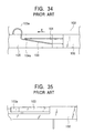
- FIGS. 34 and 35 are partial side and partial plan views, respectively, showing a state before an IC card is inserted in the card slot
- FIGS. 36 and 37 are partial side and partial plan views, respectively, showing a state in which the IC card is inserted in the card slot.
- the movable terminal 103 Before the IC card 101 is inserted in the card slot 102, the movable terminal 103 is inclined and is in elastic contact with the fixed terminal 104, and a bent leading end portion 103a thereof is placed inside the card slot 102, as shown in FIG. 34.
- Numeral 105 denotes a space portion for allowing pressure deformation of the movable terminal 103.
- the leading end portion 103a of the movable terminal 103 is pressed by the leading end portion of the IC card 101.
- the movable terminal 103 is thereby pressed down, and a leading end portion 104a of the fixed terminal 104 performs self-cleaning in sliding contact with the upper surface of the movable terminal 103, while the movable terminal 103 separates from the fixed terminal 104, so that the insertion of the IC card 101 is electrically detected.
- the IC card 101 is elastically held by repulsive force produced by pressure deformation of the movable terminal 103, and is kept in the inserted state. In this state, signal exchange (information processing) is carried out.
- the movable terminal 103 When the IC card 101 is drawn out of the card slot 102 after the completion of information processing, the movable terminal 103 returns to the state shown in FIG. 34 by its repulsive force, and makes contact again with the fixed terminal 104, whereby the ejection of the IC card 101 is detected.
- An object of the present invention is to solve such problems of the conventional art, and to provide a card connector having a simple structure and excellent operation reliability in which the loaded state of a card is stable.
- a card connector including a card detecting means, having a fixed terminal and a movable terminal, for detecting the insertion of a card, e.g., an IC card, by moving the movable terminal in response to the insertion of the card so as to switch a switch between the fixed terminal and the movable terminal, wherein resilient force of the movable terminal produced by the insertion of the card does not act in the ejecting direction of the card.
- a card detecting means having a fixed terminal and a movable terminal, for detecting the insertion of a card, e.g., an IC card, by moving the movable terminal in response to the insertion of the card so as to switch a switch between the fixed terminal and the movable terminal, wherein resilient force of the movable terminal produced by the insertion of the card does not act in the ejecting direction of the card.
- the acting direction of the resilient force of the movable terminal produced by the insertion of the card is orthogonal to the ejecting direction of the card. This further stabilizes the loaded state of the card, and improves operation reliability.
- the movable terminal has an inclined portion formed of, e.g., an actuator portion, which will be described later, and a part of the card runs onto the inclined portion so that the resilient force of the movable terminal does not act in the ejecting direction of the card.
- an inclined portion formed of, e.g., an actuator portion, which will be described later, and a part of the card runs onto the inclined portion so that the resilient force of the movable terminal does not act in the ejecting direction of the card.
- the movable terminal has an inclined portion
- the fixed terminal and the movable terminal are in contact with each other when the card is not inserted
- the movable terminal moves in contact with the fixed terminal when a part of the card impinges on the inclined portion
- the movable terminal separates from the fixed terminal when the card is inserted further and the part of the card runs onto the inclined portion.
- the effect of cleaning the contact portion therebetween is obtained.
- a stopper means formed of, e.g., a projection, which will be described later, may be provided to limit the distance over which the movable terminal moves in contact with the fixed terminal. This stopper means allows the moving distance of the movable terminal to be reduced, and therefore, the movement of the movable terminal does not have an adverse effect on switching accuracy.
- the movable terminal and the inclined portion are formed in one piece. This simplifies the structure, and reduces the costs.
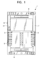
- FIG. 1 is a plan view of a housing used in an IC card connector according to a first embodiment of the present invention.
- FIG. 2 is a left side view of the housing.
- FIG. 3 is a right side view of the housing.
- FIG. 4 is a front view of the housing.
- FIG. 5 is a cross-sectional view of the housing with contact terminals mounted therein.
- FIG. 6 is a plan view of a cover used in the IC card connector.
- FIG. 7 is a left side view of the cover.
- FIG. 8 is a right side view of the cover.
- FIG. 9 is a front view of the cover.
- FIG. 10 is a cross-sectional view showing the state of the contact terminals before an IC card is inserted.
- FIG. 11 is a cross-sectional view showing the state of the contact terminals after the IC card is inserted.
- FIG. 12 is a plan view showing a part of the housing having a normally-closed detection switch in the IC card connector, and a part of the cover for covering the housing.
- FIG. 13 is a partial sectional view showing the state of a fixed terminal before the cover is mounted.
- FIG. 15 is a side view of the fixed terminal used in the normally closed detection switch.
- FIG. 16 is a side view showing the positional relationship between the fixed terminal and a movable terminal before the cover is mounted.
- FIG. 17 is a plan view showing the placement of the fixed terminal and the movable terminal.
- FIG. 18 is a cross-sectional view showing the normally closed detection switch in a standby state.
- FIG. 19 is a cross-sectional view showing the state of the normally closed detection switch during the insertion of the IC card.
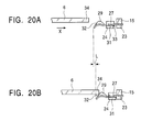
- FIGS. 20A and 20B are explanatory views showing how the movable terminal moves from when the normally closed detection switch is in the standby state and until when the IC card is being inserted.
- FIG. 21 is a cross-sectional view showing the state of the normally closed detection switch during the insertion of the IC card.
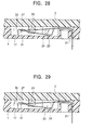
- FIG. 29 is a cross-sectional view showing the state of the normally closed detection switch during the insertion of an IC card.
- FIG. 32 is a cross-sectional view showing the state of the normally closed detection switch when the insertion of the IC card is completed.
- FIG. 35 is a partial plan view showing the state before the IC card is inserted in the card slot.
- the cover 2 is provided with an inclined face 12 formed at its right side end so as to guide the IC card 6 that is being inserted, two holes 13 on its upper surface, and retaining frames 14 projecting from its left side.
- a projection 15 is formed adjacent to one of the retaining frames 14.
- a receiving portion 16 having a flat lower surface is provided at the position opposed to the contact portions 10 of the contact terminals 11.
- FIGS. 10 and 11 are cross-sectional views of the IC card connector.
- FIG. 10 shows a state before the IC card 6 is inserted
- FIG. 11 shows a state when the insertion of the IC card 6 has been completed.
- the cover 2 is placed on the housing 1, the pins 8 of the housing 1 are inserted in the holes 13 of the cover 2, and the retaining frames 14 of the cover 2 are engaged with the retaining claws 9 of the housing 1, whereby the housing 1 and the cover 2 are combined into one, as shown in FIG. 10.
- a card slot 19 having a card insertion opening 18 is formed between the housing 1 and the cover 2, the inclined faces 7 and 12 are placed to face each other at the card insertion opening 18, and the contact portions 10 of the contact terminals 11 are brought into elastic contact with the lower surface of the receiving portion 16.
- the contact terminals 11 are pressed down by the leading end portion of the IC card 6, and make contact with the contact patterns of the IC card 6 at an inserted position of the IC card 6 (see FIG. 11), whereby signal exchange is made possible, and the IC card 6 is elastically clamped between the contact terminals 11 and the receiving portion 16.
- a round or inclined guide portion 20 is formed at the end of the receiving portion 16 on the side of the card insertion opening 18 in order to achieve smooth insertion of the IC card 6.
- FIG. 12 is a plan view showing a part of the housing having a normally closed detection switch, and a part of the cover for covering the housing
- FIG. 13 is a partial sectional view showing a state before the cover is mounted
- FIG. 14 is a partial sectional view showing a state in which the cover has been mounted
- FIG. 15 is a side view of a fixed terminal
- FIG. 16 is a side view showing the positional relationship between the fixed terminal and a movable terminal before the cover is mounted.
- the concave detection switch mounting portion 17 is provided at the position of the housing 1 adjacent to the card slot 19, in which a fixed terminal mounting hole 21 and a movable terminal mounting hole 22 are formed side by side.
- a fixed terminal 23 and a movable terminal 24 are fixed in parallel in the mounting holes 21 and 22, respectively, in a cantilevered manner to constitute a normally closed detection switch.
- the fixed terminal 23 includes a fixed portion 25 that is press-fitted in the mounting hole 21 and projects from the lower surface of the housing 1, a middle portion 26 having a stepped bent portion at the midpoint thereof so as to extend from the fixed portion 25 and to be slightly inclined upward from the bent portion toward the leading end, and a contact portion 27 provided at the leading end of the middle portion 26 so as to extend toward the movable terminal 24, as shown in FIG. 12.
- the fixed portion 28 of the movable terminal 24 is press-fitted in the mounting hole 22, thereby fixing the movable terminal 24.
- the detection switch mounting portion 17 is provided at the position adjacent to the card slot 19, and is isolated from the card slot 19 by a partition 36 formed therebetween.
- the partition 36 has a cutout portion 37, from which only the actuator portion 29 of the movable terminal 24 protrudes toward the card slot 19.
- the fixed portion 25 of the fixed terminal 23 is press-fitted in the mounting hole 21 at a short distance 31 from the movable terminal 24, and the fixed terminal 23 is fixed in parallel with the movable terminal 24.
- the contact portion 27 of the fixed terminal 23 is placed above the contact portion 31 of the movable terminal 24, and is separate from the contact portion 31, as shown in FIG. 16.
- the projection 15 formed in the cover 2 is positioned opposed to the middle portion 26 of the fixed terminal 23, as shown in FIGS. 13, 14, and 17.
- the fixed terminal 23 is pressed down by the projection 15, and the contact portion 27 of the fixed terminal 23 is brought into elastic contact with the contact portion 31 of the movable terminal 24, whereby the normally closed switch is placed into a standby state (on-state) (see FIGS. 18 and 20A).
- the movable terminal 24 is not shown in FIGS. 13 and 14 in order to prevent the figures from being complicated.
- FIGS. 18 and 20A show the state before the IC card 6 is inserted.
- a leading end portion 34 of the IC card 6 impinges on the pressing face 32 of the actuator portion 29 of the movable terminal 24. Since the movable terminal 24 is turnable about the fixed portion 28 in the direction of the arrow Z, as shown in FIG.
- the movable terminal 24 turns about the fixed portion 28 by a distance L (corresponding to a space 33) toward the projection 15 (in the card inserting direction, i.e., the X-direction), and impinges on the projection 15 (see FIG. 20B).
- the movable terminal 24 is pressed down by the IC card 6 via the actuator portion 29, as shown in FIG. 23B.
- Resilient force resulting from the press acts in the direction of the arrow F, and is orthogonal to the ejecting direction Y of the IC card 6.
- the resilient force of the movable terminal 24 does not act in the ejecting direction Y of the IC card 6.
- This embodiment is different from the first embodiment in that elastic force of a fixed terminal 23 is always directed downward, and is designed to be sufficiently smaller than that of a movable terminal 24.
- FIGS. 28 and 30A The upper side of the fixed terminal 23 raised by the movable terminal 24 is positioned by a projection 15 formed in a cover 2.
- a support portion 35 bent downward is provided at the leading end of the fixed terminal 23 on the side of the contact portion 27.
- IC card is used in the above embodiments, it is to be understood that the present invention is not limited to the above embodiments, and is also applicable to cases in which other cards, for example, a magnetic card and an optical card, are used.
Landscapes
- Engineering & Computer Science (AREA)
- Artificial Intelligence (AREA)
- Computer Vision & Pattern Recognition (AREA)
- Physics & Mathematics (AREA)
- General Physics & Mathematics (AREA)
- Theoretical Computer Science (AREA)
- Coupling Device And Connection With Printed Circuit (AREA)
- Details Of Connecting Devices For Male And Female Coupling (AREA)
Applications Claiming Priority (2)
| Application Number | Priority Date | Filing Date | Title |
|---|---|---|---|
| JP10215980A JP2000048915A (ja) | 1998-07-30 | 1998-07-30 | カード用コネクタ |
| JP21598098 | 1998-07-30 |
Publications (2)
| Publication Number | Publication Date |
|---|---|
| EP0977140A2 true EP0977140A2 (de) | 2000-02-02 |
| EP0977140A3 EP0977140A3 (de) | 2001-11-07 |
Family
ID=16681429
Family Applications (1)
| Application Number | Title | Priority Date | Filing Date |
|---|---|---|---|
| EP99305421A Withdrawn EP0977140A3 (de) | 1998-07-30 | 1999-07-08 | Kartenverbinder mit Mitteln zur Erkennung der Karteneinführung |
Country Status (4)
| Country | Link |
|---|---|
| US (1) | US6267619B1 (de) |
| EP (1) | EP0977140A3 (de) |
| JP (1) | JP2000048915A (de) |
| TW (1) | TW431039B (de) |
Families Citing this family (11)
| Publication number | Priority date | Publication date | Assignee | Title |
|---|---|---|---|---|
| JP3333481B2 (ja) * | 1999-11-16 | 2002-10-15 | 山一電機株式会社 | カードコネクタのカード認識スイッチ |
| JP3821648B2 (ja) * | 2001-01-15 | 2006-09-13 | アルプス電気株式会社 | カード用コネクタ装置 |
| TW496595U (en) * | 2001-03-20 | 2002-07-21 | Hon Hai Prec Ind Co Ltd | Electronic card connector |
| JP6081719B2 (ja) * | 2012-07-02 | 2017-02-15 | タイコエレクトロニクスジャパン合同会社 | カードコネクタ |
| CN203085808U (zh) * | 2013-02-20 | 2013-07-24 | 莫列斯公司 | 电连接器 |
| US9275260B2 (en) | 2013-02-20 | 2016-03-01 | Molex, Llc | Low profile connector |
| CN203135146U (zh) | 2013-02-20 | 2013-08-14 | 莫列斯公司 | 电连接器 |
| JP5970391B2 (ja) * | 2013-02-25 | 2016-08-17 | タイコエレクトロニクスジャパン合同会社 | カードコネクタ |
| US9969042B2 (en) | 2013-05-16 | 2018-05-15 | Kreg Enterprises, Inc. | Ratcheting quick-adjust drilling jig |
| JP6424328B2 (ja) * | 2014-12-12 | 2018-11-21 | 旭精工株式会社 | カード処理装置 |
| CN114333467B (zh) * | 2021-12-03 | 2024-04-30 | 苏州通富超威半导体有限公司 | 一种更换cpu测试插槽的员工培训装置及方法 |
Family Cites Families (11)
| Publication number | Priority date | Publication date | Assignee | Title |
|---|---|---|---|---|
| FR2623314B1 (fr) | 1987-11-13 | 1991-06-14 | Cit Alcatel | Cadre de contact pour lecteur de carte a puce, avec contact de fin de course |
| FR2638293B1 (fr) * | 1988-10-26 | 1991-01-18 | Itt Composants Instr | Connecteur electrique pour cartes a memoire electronique, procede de realisation d'un tel connecteur et dispositif de lecture-ecriture integrant un tel connecteur |
| DE3943703C2 (de) * | 1989-09-21 | 2001-06-21 | Amphenol Tuchel Elect | Chipkartenleser |
| US5511986A (en) * | 1994-02-23 | 1996-04-30 | Molex Incorporated | IC pack connector with detect switch |
| DE29618976U1 (de) * | 1996-11-04 | 1997-01-16 | Thomas & Betts GmbH, 63329 Egelsbach | Lesegerät für Chipkarten |
| JPH1197109A (ja) * | 1997-09-16 | 1999-04-09 | Alps Electric Co Ltd | Icカード用コネクタ |
| TW383933U (en) * | 1998-03-03 | 2000-03-01 | Hon Hai Prec Ind Co Ltd | Electrical connector |
| TW438096U (en) * | 1998-05-08 | 2001-05-28 | Hon Hai Prec Ind Co Ltd | Electronic card connector |
| JP3483467B2 (ja) * | 1998-05-18 | 2004-01-06 | アルプス電気株式会社 | Icカード用コネクタ |
| TW374506U (en) * | 1998-06-06 | 1999-11-11 | Hon Hai Prec Ind Co Ltd | Electronic card base board connector with the switching device |
| US6004155A (en) * | 1998-07-28 | 1999-12-21 | Hon Hai Precision Ind. Co., Ltd. | Card connector |
-
1998
- 1998-07-30 JP JP10215980A patent/JP2000048915A/ja active Pending
-
1999
- 1999-07-06 TW TW088111451A patent/TW431039B/zh not_active IP Right Cessation
- 1999-07-08 EP EP99305421A patent/EP0977140A3/de not_active Withdrawn
- 1999-07-30 US US09/364,586 patent/US6267619B1/en not_active Expired - Fee Related
Also Published As
| Publication number | Publication date |
|---|---|
| EP0977140A3 (de) | 2001-11-07 |
| TW431039B (en) | 2001-04-21 |
| JP2000048915A (ja) | 2000-02-18 |
| US6267619B1 (en) | 2001-07-31 |
Similar Documents
| Publication | Publication Date | Title |
|---|---|---|
| US6399906B1 (en) | Switch for a card connector | |
| CN100521394C (zh) | 卡连接器 | |
| JP3821648B2 (ja) | カード用コネクタ装置 | |
| EP0704813B1 (de) | Informationsverarbeitungsvorrichtung für eine IC-Karte | |
| EP1152499B1 (de) | Schreibschutz-schalter für kartenverbinder | |
| US6267619B1 (en) | Card connector having means for detecting insertion of a card | |
| WO1998043199A1 (en) | Card reader connector having a separable cover | |
| JP2000506638A (ja) | スマートカード及びスマートカード用コネクタ | |
| JP3961224B2 (ja) | カード用コネクタ装置 | |
| JPH08511115A (ja) | Simカード及び標準カード用のsmtリーダー | |
| US6769614B2 (en) | Magnetic card reader | |
| JPH09319838A (ja) | スマートカードシステム | |
| US6174186B1 (en) | Card connector | |
| CN101997242B (zh) | 连接器以及检测开关 | |
| JPH10240874A (ja) | カードリーダ | |
| JP2003036934A (ja) | カードコネクタ | |
| EP0293888B1 (de) | Chip-Kartenleser | |
| US7372136B2 (en) | Chip card retaining mechanism | |
| US20070131777A1 (en) | Chip card retaining mechanism | |
| JP3807730B2 (ja) | カードコネクタ | |
| US5282113A (en) | Memory card with a plurality of contact spaces | |
| KR100469668B1 (ko) | 카드커넥터 | |
| JP3683393B2 (ja) | 検出スイッチ | |
| JP3765708B2 (ja) | カード用コネクタ装置 | |
| JP2006172746A (ja) | カード用コネクタ装置およびカード |
Legal Events
| Date | Code | Title | Description |
|---|---|---|---|
| PUAI | Public reference made under article 153(3) epc to a published international application that has entered the european phase |
Free format text: ORIGINAL CODE: 0009012 |
|
| AK | Designated contracting states |
Kind code of ref document: A2 Designated state(s): AT BE CH CY DE DK ES FI FR GB GR IE IT LI LU MC NL PT SE Kind code of ref document: A2 Designated state(s): DE FR GB |
|
| AX | Request for extension of the european patent |
Free format text: AL;LT;LV;MK;RO;SI |
|
| PUAL | Search report despatched |
Free format text: ORIGINAL CODE: 0009013 |
|
| AK | Designated contracting states |
Kind code of ref document: A3 Designated state(s): AT BE CH CY DE DK ES FI FR GB GR IE IT LI LU MC NL PT SE |
|
| AX | Request for extension of the european patent |
Free format text: AL;LT;LV;MK;RO;SI |
|
| 17P | Request for examination filed |
Effective date: 20011207 |
|
| AKX | Designation fees paid |
Free format text: DE FR GB |
|
| 17Q | First examination report despatched |
Effective date: 20020821 |
|
| GRAP | Despatch of communication of intention to grant a patent |
Free format text: ORIGINAL CODE: EPIDOSNIGR1 |
|
| STAA | Information on the status of an ep patent application or granted ep patent |
Free format text: STATUS: THE APPLICATION IS DEEMED TO BE WITHDRAWN |
|
| 18D | Application deemed to be withdrawn |
Effective date: 20070508 |