EP0977252B1 - Selektive Verlegung von Elementen von einem Träger zu einem anderen Träger - Google Patents
Selektive Verlegung von Elementen von einem Träger zu einem anderen Träger Download PDFInfo
- Publication number
- EP0977252B1 EP0977252B1 EP99401896A EP99401896A EP0977252B1 EP 0977252 B1 EP0977252 B1 EP 0977252B1 EP 99401896 A EP99401896 A EP 99401896A EP 99401896 A EP99401896 A EP 99401896A EP 0977252 B1 EP0977252 B1 EP 0977252B1
- Authority
- EP
- European Patent Office
- Prior art keywords
- elements
- face
- transferred
- support
- bonding
- Prior art date
- Legal status (The legal status is an assumption and is not a legal conclusion. Google has not performed a legal analysis and makes no representation as to the accuracy of the status listed.)
- Expired - Lifetime
Links
Images

Classifications
-
- H—ELECTRICITY
- H10—SEMICONDUCTOR DEVICES; ELECTRIC SOLID-STATE DEVICES NOT OTHERWISE PROVIDED FOR
- H10W—GENERIC PACKAGES, INTERCONNECTIONS, CONNECTORS OR OTHER CONSTRUCTIONAL DETAILS OF DEVICES COVERED BY CLASS H10
- H10W74/00—Encapsulations, e.g. protective coatings
- H10W74/01—Manufacture or treatment
- H10W74/019—Manufacture or treatment using temporary auxiliary substrates
-
- H—ELECTRICITY
- H10—SEMICONDUCTOR DEVICES; ELECTRIC SOLID-STATE DEVICES NOT OTHERWISE PROVIDED FOR
- H10P—GENERIC PROCESSES OR APPARATUS FOR THE MANUFACTURE OR TREATMENT OF DEVICES COVERED BY CLASS H10
- H10P72/00—Handling or holding of wafers, substrates or devices during manufacture or treatment thereof
- H10P72/70—Handling or holding of wafers, substrates or devices during manufacture or treatment thereof for supporting or gripping
- H10P72/74—Handling or holding of wafers, substrates or devices during manufacture or treatment thereof for supporting or gripping using temporarily an auxiliary support
-
- H—ELECTRICITY
- H10—SEMICONDUCTOR DEVICES; ELECTRIC SOLID-STATE DEVICES NOT OTHERWISE PROVIDED FOR
- H10W—GENERIC PACKAGES, INTERCONNECTIONS, CONNECTORS OR OTHER CONSTRUCTIONAL DETAILS OF DEVICES COVERED BY CLASS H10
- H10W72/00—Interconnections or connectors in packages
- H10W72/30—Die-attach connectors
-
- H—ELECTRICITY
- H10—SEMICONDUCTOR DEVICES; ELECTRIC SOLID-STATE DEVICES NOT OTHERWISE PROVIDED FOR
- H10P—GENERIC PROCESSES OR APPARATUS FOR THE MANUFACTURE OR TREATMENT OF DEVICES COVERED BY CLASS H10
- H10P72/00—Handling or holding of wafers, substrates or devices during manufacture or treatment thereof
- H10P72/70—Handling or holding of wafers, substrates or devices during manufacture or treatment thereof for supporting or gripping
- H10P72/74—Handling or holding of wafers, substrates or devices during manufacture or treatment thereof for supporting or gripping using temporarily an auxiliary support
- H10P72/7428—Handling or holding of wafers, substrates or devices during manufacture or treatment thereof for supporting or gripping using temporarily an auxiliary support used to support diced chips prior to mounting
-
- H—ELECTRICITY
- H10—SEMICONDUCTOR DEVICES; ELECTRIC SOLID-STATE DEVICES NOT OTHERWISE PROVIDED FOR
- H10P—GENERIC PROCESSES OR APPARATUS FOR THE MANUFACTURE OR TREATMENT OF DEVICES COVERED BY CLASS H10
- H10P72/00—Handling or holding of wafers, substrates or devices during manufacture or treatment thereof
- H10P72/70—Handling or holding of wafers, substrates or devices during manufacture or treatment thereof for supporting or gripping
- H10P72/74—Handling or holding of wafers, substrates or devices during manufacture or treatment thereof for supporting or gripping using temporarily an auxiliary support
- H10P72/7434—Handling or holding of wafers, substrates or devices during manufacture or treatment thereof for supporting or gripping using temporarily an auxiliary support used in a transfer process involving at least two transfer steps, i.e. including an intermediate handle substrate
-
- H—ELECTRICITY
- H10—SEMICONDUCTOR DEVICES; ELECTRIC SOLID-STATE DEVICES NOT OTHERWISE PROVIDED FOR
- H10W—GENERIC PACKAGES, INTERCONNECTIONS, CONNECTORS OR OTHER CONSTRUCTIONAL DETAILS OF DEVICES COVERED BY CLASS H10
- H10W72/00—Interconnections or connectors in packages
- H10W72/01—Manufacture or treatment
- H10W72/0198—Manufacture or treatment batch processes
-
- H—ELECTRICITY
- H10—SEMICONDUCTOR DEVICES; ELECTRIC SOLID-STATE DEVICES NOT OTHERWISE PROVIDED FOR
- H10W—GENERIC PACKAGES, INTERCONNECTIONS, CONNECTORS OR OTHER CONSTRUCTIONAL DETAILS OF DEVICES COVERED BY CLASS H10
- H10W72/00—Interconnections or connectors in packages
- H10W72/071—Connecting or disconnecting
- H10W72/073—Connecting or disconnecting of die-attach connectors
-
- H—ELECTRICITY
- H10—SEMICONDUCTOR DEVICES; ELECTRIC SOLID-STATE DEVICES NOT OTHERWISE PROVIDED FOR
- H10W—GENERIC PACKAGES, INTERCONNECTIONS, CONNECTORS OR OTHER CONSTRUCTIONAL DETAILS OF DEVICES COVERED BY CLASS H10
- H10W72/00—Interconnections or connectors in packages
- H10W72/071—Connecting or disconnecting
- H10W72/073—Connecting or disconnecting of die-attach connectors
- H10W72/07331—Connecting techniques
- H10W72/07337—Connecting techniques using a polymer adhesive, e.g. an adhesive based on silicone or epoxy
Definitions
- the present invention relates to the selective transfer of elements from a transfer medium to a receiving medium.
- the invention enables the transfer of chips, for example the transfer of 1 cm 2 chips from the surface of their initial substrate onto glass or onto a transparent substrate. It also allows the transfer of optoelectronic components such as VCSELs (vertical cavity lasers) or small pieces of III-V semiconductor from their initial substrate onto silicon wafers prepared by microelectronics techniques to obtain semiconductor elements. III-V on silicon. In this case in general, the size of the chips is smaller, for example of the order of 1 mm 2 or less.
- Molecular adhesion comprises two types of bonding: hydrophilic bonding and hydrophobic bonding.
- hydrophilic bonding results from the evolution of -OH interactions on the surface of a structure towards the formation of Si-O-Si bonds for example in the case of silicon oxide.
- the forces associated with this type of interaction are strong.
- the bonding energy of the order of 100 mJ / m 2 at room temperature, reaches 500 mJ / m 2 after annealing at 400 ° C for 30 minutes (values obtained for a SiO 2 bonding native or hydrophilic - SiO 2 thermal unpolished).
- the bonding energy is generally determined by the blade method disclosed by WP MASZARA et al. in the article "Bonding of silicon wafers for silicon-on-insulator" published in J. Appl. Phys. 64 (10), November 15, 1988, pages 4943-4950. .
- the bonding energy is of the order of 1 J / m 2 for annealing under the same conditions.
- the present invention has been designed to provide selective element transfer from a first medium to a receiving medium. To achieve this result, it can in particular implement the technique of molecular adhesion.
- the joining of the face of the initial substrate comprising said elements with the transfer medium is obtained by molecular adhesion.
- this molecular adhesion it is advantageous for this molecular adhesion to be carried out by one or more treatments of the faces to be joined to the initial substrate and / or of the transfer medium so as to control the hydrophilicity and / or the hydrophobicity and / or a microroughness. satisfactory for obtaining said defined adhesion energy.
- a heat treatment can be implemented, globally or locally, to contribute to obtaining this adhesion energy.
- the elements may include a layer, called the barrier layer, by which they are connected to the initial substrate.
- the elimination of the initial substrate can be obtained by one or more of: rectification, chemical etching of the initial substrate and / or the barrier layer, polishing, separation following a heat treatment along an ion implant induced cleavage plane.
- the step of defining at least one element to be transferred may comprise the isolation of the element to be transferred.
- this isolation can be achieved by chemical etching, blade cutting, laser etching or any other cutting means.
- this isolation is achieved by etching, it is conducted so as to form etching feet near the transfer medium.
- the adhering contact of the second face of said element to be transferred with the receiving medium can be obtained by molecular adhesion.
- a heat treatment may be implemented, globally or locally, to contribute to obtaining the adhesion energy defined between the second face of said element to be transferred and the receiving medium.
- the adhesion by molecular adhesion of the second face of said element to be transferred and of the receiving medium can be obtained by a treatment of said second face and / or all or part of the receiving medium.
- the retaining means may consist of treating the elements not to be transferred and / or zones of the receiving support not able to receive elements so that there is no adhesion between the elements not to be transferred and the support reception.
- the treatment conferring said retaining means may be chosen from one or more of the following treatments: hydrophilicity, hydrophobicity, roughness, heat treatment, surface removal.
- the retaining means may consist in treating the second face of these elements not to be transferred for confer a hydrophobic bonding quality with the receiving support, the second face of said element to be transferred being treated to give it a hydrophilic bonding quality, the receiving support providing the second face of each element a hydrophilic bonding quality.
- They may also consist in treating the zone of the receiving support facing the second face of a non-transferable element in order to confer on it a quality of hydrophobic bonding, the zone of the receiving support facing the second face of said element transferring being treated to give it a hydrophilic bonding quality, all the second faces of the elements being treated to give them a hydrophilic bonding quality.
- a variant of the method therefore consists in locally carrying out the heat treatment so as to heat only the areas where it is desired to transfer between the elements and the receiving medium.
- the heating may be performed using a laser or a heating tip.
- said retaining means may consist of either performing a local heat treatment, or to provide an absence of mechanical contact between the second face of the elements not to be transferred and the receiving medium. For example, this absence of contact will be related to a local withdrawal on the second face and / or on the receiving medium.
- the separation of the transfer medium and the receiving medium is consecutive to a mechanical force exerted between these supports and consisting of a tensile force and / or a shear force and / or a bending force, all of which can be assisted. thermally.
- the method according to the invention applies in particular to the case where said elements comprise electronic components, for example semiconductor chips and / or passive elements.
- said elements comprise electronic components, for example semiconductor chips and / or passive elements.
- the cited elements having applications in microelectronics, optoelectronics or even in the field of superconductors.
- FIG. 1 shows a substrate 2, called an initial substrate, for example made of silicon, on which semiconductor chips 4 have been developed according to the techniques known to those skilled in the art.
- a barrier layer 6, for example silicon oxide, may optionally be provided between the semiconductor chips 4 and the initial substrate 2. This stop layer provides the advantage of better homogeneity of the transfer thereafter because it is a barrier layer for example with respect to chemical etching and / or selective plasma etching.
- the semiconductor chips 4 are intended to be selectively transferred. To do this, the surface of the initial substrate presenting the chips will be prepared to allow hydrophilic bonding with controlled bonding energy.
- This surface preparation illustrated in FIG. 2, can comprise the deposition of a layer 8 in which the semiconductor chips 4 are embedded.
- the layer 8 may be a silicon oxide layer having undergone a planarization operation if the topology of its free surface requires it.
- the bonding energy of a surface can be controlled by varying the roughness of this surface.
- a roughness of the order of 6 angstroms in root mean square obtained by HF etching provides a adhesive energy of the order of 250 mJ / m 2 after annealing at a temperature of 400 ° C for 30 minutes.
- a transfer support or handle 10 is glued to the free face of the layer 8. If the faces glued together of the layer 8 and the transfer support 10 each have a roughness of about 6 angstroms rms, the bonding energy obtained is of the order of 250 mJ / m 2 .
- the handle 10 may be transparent (for example glass or pure silica).
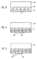
- the initial substrate is then removed (see Figure 4) by a conventional method or a combination of conventional methods.
- Mechanical rectification, polishing or separation obtained after thermal treatment along an ion implantation induced cleavage plane may be mentioned. This latter method is particularly described in the document FR-A-2,681,472 . This achievement can also be obtained by chemical, reactive, selective or ultrasonic etching.
- the elements to be transferred are then delimited. For example, this can be done by delineation trenches by chemical or dry etching, by a circular saw, by a disc saw, by ultrasonic cutting. This is shown in FIG. 5, where trenches 12, cut to the transfer medium 10, delimit elements 14, each element comprising a semiconductor chip 4.
- the free surface of the elements 14 is then prepared (for example: surface cleaning and / or deposition of a very thin film of oxide) to have a very good hydrophilic bonding.
- hydrophilic preparation is meant any surface treatment which makes it possible to obtain OH groups on the surface.
- the free surface of the elements that must not be transferred is treated to make it hydrophobic.
- This treatment therefore makes it possible to delimit hydrophilic and hydrophobic zones.
- the zones can be rendered hydrophobic for example by means of an HF treatment in the case of silicon oxide, by a plasma treatment or by another treatment localized chemical.
- an object that makes it possible to modify the hydrophilicity when it is brought into contact. Examples include the use of a Teflon ® tip whose size is equal to the area to treat.
- FIG. 6 symbolically illustrates such a treatment.
- One of the elements 14 is shown with a hydrophilic surface treatment 16 while the other elements 14 have hydrophobic surfaces.
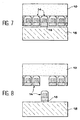
- the transfer support 10 provided with the elements 14 can be glued to the receiving support 18 which has been cleaned in such a way that the surface it presents to the elements 14 is hydrophilic.
- the bonding energy between the elements 14 and the transfer medium 10 is of the order of 250 mJ / m 2 .
- the bonding energy between the element 14 having the hydrophilic surface treatment 16 and the receiving support 18 is greater than 500 mJ / m 2 .
- the bonding energy between the other elements 14 having a hydrophobic surface treatment and the hydrophilic surface of the receiving support 18 is of the order of 100 mJ / m 2 . It is recalled that the bonding forces can be controlled by means of a heat treatment, for example at a temperature of 400 ° C. for 30 minutes.
- the method according to the invention allows precise positioning of an element (comprising a semiconductor chip) on its new support using standard lithography means or, preferably, using a transparent handle by optical alignment. or with a microcrystalline handle for X-ray alignment. It allows the transfer of elements in several times or the transfer of several elements at a time. It also allows the transfer of any type of solid material.
- the size of the semiconductor chips that can be transferred can range from a few tens of square micrometers to several square centimeters.
- the transfer of the elements is ensured only in the areas where the bonding is effective by contact of hydrophilic surfaces between the elements and the receiving medium.
- the surface of the elements to be transferred can be made hydrophilic as well as the corresponding surface of the receiving medium while the surface of the elements not to be transferred is rendered hydrophobic (as described above).
- the surface of all the elements is made hydrophilic as well as the corresponding surface of the receiving medium facing the elements to be transferred while the areas of the receiving medium facing the elements not to be transferred are rendered hydrophobic.
- the surface of all the elements is made hydrophilic as well as the surface of the receiving support. Items not to be transferred are indented. In this case, only the elements to be transferred come into contact with the reception medium.
- the indentation can be obtained by chemical etching and / or dry etching, for example, if one is in the presence of SiO 2 by chemical etching with HF. Lithography can be done to delimit the areas to be treated.
- the surface of all the elements is rendered hydrophilic as well as the surface of the receiving medium whose zones opposite the elements not to be transferred are recessed.
- the method according to the invention applies to the individual transfer or the collective transfer of elements from their initial support to their receiving medium. For example, if a substrate has 150 transferable semiconductor chips and it is desired to transfer only 50 chips at a time on the receiving medium, it is possible, by calculating the pitch between the chips, to transfer first 50 chips, then shift one of the media of the defined step, transfer again 50 chips, perform a new shift of the defined step and transfer again the last 50 chips.
- Another variant of the process consists in using chemical or physical treatments which strongly modify the roughness locally. For example, if the areas to be bonded by chemical cleaning are roughened to obtain roughnesses of the order of 15 angstroms in root mean square, even after hydrophilic cleaning, the bonding forces will be so small that will not occur in areas of high roughness.
- This selective processing can be performed on the elements to be transferred or on the receiving medium.
Landscapes
- Recrystallisation Techniques (AREA)
- Jigs For Machine Tools (AREA)
- Weting (AREA)
- Pressure Welding/Diffusion-Bonding (AREA)
- Micromachines (AREA)
Claims (23)
- Verfahren für den selektiven Transfer von Elementen (14) von einem Transferträger (10) zu einem Empfangsträger (18), wobei die Elemente (14) mit einer ersten Seite und einer definierten Adhäsionsenergie an dem Transferträger (10) haften, jedes der Elemente (14) eine zweite Seite zur Herstellung des Kontakts mit dem Empfangsträger (18) aufweist, das Verfahren dabei die folgenden Schritte umfasst:- Definition wenigstens eines zu transferierenden Elements unter den genannten Elementen (14), was die Trennung des genannten zu transferierenden Elements von den nicht zu transferierenden Elementen impliziert,- Behandlung der zweiten Seite des genannten zu transferierenden Elements (14), um ihr eine Adhäsionsenergie in Verbindung mit dem Empfangsträger (18) zu verleihen, die größer ist als die Adhäsionsenergie seiner ersten Seite in Verbindung mit dem Transferträger (10), wobei Rückhaltemittel vorgesehen sind, um die nicht zu transferierenden Elemente am Transferträger (10) festzuhalten,- Herstellung des Haftkontakts zwischen der zweiten Seite des zu transferierenden Elements (14) und dem Empfangsträger (18),- Trennung bzw. Entfernung des Transferträgers (10) vom Empfangsträger (18), um das Transferieren des genannten zu transferierenden Elements zum Empfangsträger und das Festhalten der anderen Elemente am Transferträger zu realisieren.
- Verfahren nach Anspruch 1, dadurch gekennzeichnet, dass es die folgenden vorausgehenden Schritte umfasst:- Bildung der genannten Elemente auf einer Seite eines Initialsubstrats (2), wobei die Elemente mit ihrer zweiten Seite auf der genannten Seite des Initialsubstrats (2) ruhen,- Verbindung der die genannten Elemente umfassenden Seite des Initialsubstrats mit dem Transferträger (10), so dass die Elemente mit ihrer ersten Seite entsprechend der genannten definierten Adhäsionsenergie daran haften,- Eliminierung des Initialsubstrats (2), so dass die Elemente ihre zweite Seite präsentieren.
- Verfahren nach Anspruch 2, dadurch gekennzeichnet, dass die Verbindung der die genannten Elemente umfassenden Seite des Initialsubstrats mit dem Transferträger (10) auf Molekularadhäsion beruht.
- Verfahren nach Anspruch 3, dadurch gekennzeichnet, dass diese Molekularadhäsion durch eine oder mehrere Behandlungen der zu verbindenden Seiten des Initialsubstrats (2) und/oder des Transferträgers (10) realisiert wird, um die Hydrophilie und/oder die Hydrophobie und/oder eine zufriedenstellende Mikrorauhigkeit zur Erzeugung der genannten definierten Adhäsionsenergie zu kontrollieren.
- Verfahren nach Anspruch 3, dadurch gekennzeichnet, dass eine Wärmebehandlung durchgeführt wird, global oder lokal, um zu der Erzeugung der definierten Adhäsionsenergie zwischen der die genannten Elemente umfassenden Seite des Substrats (2) und dem Transferträger (10) beizutragen.
- Verfahren nach einem der Ansprüche 2 bis 5, dadurch gekennzeichnet, dass die Elemente eine Sperrschicht genannte Schicht (6) umfassen, durch die sie mit dem Initialsubstrat (2) verbunden sind.
- Verfahren nach einem der Ansprüche 2 bis 6, dadurch gekennzeichnet, dass man zur Eliminierung des Initialsubstrats (2) eine oder mehrere Techniken unter folgenden auswählt: Schleifen, chemisches Ätzen des Initialsubstrats und/oder der Sperrschicht, Polieren, Abtrennen infolge einer thermischen Behandlung längs einer durch Ionenimplantation erzeugten Spaltungsebene.
- Verfahren nach einem der Ansprüche 1 bis 7, dadurch gekennzeichnet, dass - da die Elemente (14) auf dem Transferträger eine kontinuierliche Schicht bilden, der Schritt zur Definition wenigstens eines zu transferierenden Elements die Isolierung des zu transferierenden Elements umfasst.
- Verfahren nach Anspruch 8, dadurch gekennzeichnet, dass diese Isolierung durch eine der folgenden Techniken erfolgt: chemisches Ätzen, Messerschneiden, L.aserstrahlschneidon.
- Verfahren nach Anspruch 9, dadurch gekennzeichnet, dass - wenn die Isolierung durch Ätzen erfolgt, dieses so durchgeführt wird, dass sich nahe bei dem Transferträger (10) Ätzfüße bilden.
- Verfahren nach einem der Ansprüche 1 bis 10, dadurch gekennzeichnet, dass die Herstellung des Haftkontakts der zweiten Seite des genannten zu transferierenden Elements (14) mit dem Empfangsträger (18) durch Molekularadhäsion erlangt wird.
- Verfahren nach Anspruch 11, dadurch gekennzeichnet, dass eine thermische Behandlung durchgeführt wird, global oder lokal, um zu der Erzeugung der definierten Adhäsionsenergie zwischen der zweiten Seite des genannten zu transferierenden Elements und dem Empfangsträger beizutragen.
- Verfahren nach Anspruch 11, dadurch gekennzeichnet, dass die Adhäsion mittels Molekularhaftung der zweiten Seite des genannten zu transferierenden Elements (14) und des Empfangsträgers durch eine Behandlung der genannten zweiten Seite und/oder der Gesamtheit oder eines Teils des Empfangsträgers (18) erlangt wird.
- Verfahren nach einem der vorangehenden Ansprüche, dadurch gekennzeichnet, dass die genannten Rückhaltemittel aus einer Behandlung der nicht zu transferierenden Elemente und/oder von nicht zum Empfang von Elementen geeigneten bzw. bestimmten Zonen des Empfangsträgers bestehen, so dass es keine Adhäsion zwischen den nicht zu transferierenden Elementen und dem Empfangsträger gibt.
- Verfahren nach Anspruch 14, dadurch gekennzeichnet, dass die genannten Rückhaltemittel aus einer Modifizierung der Oberfläche der nicht zu transferierenden Elemente und/oder der Oberfläche der nicht zum Empfang von Elementen geeigneten bzw. bestimmten Zonen des Empfangsträgers bestehen, um die Adhäsionsenergie zwischen den nicht zu transferierenden Elementen und dem Empfangsträger niedriger als die Adhäsionsenergie zwischen den zu transferierenden Elementen und dem Empfangsträger und niedriger als die Adhäsionsenergie zwischen den ersten Seiten der Elemente und dem Transferträger zu halten.
- Verfahren nach Anspruch 14, dadurch gekennzeichnet, dass man für die die genannten Rückhaltemittel realisierende Behandlung eine oder mehrere der folgenden Behandlungen wählt: Hydrophilie, Hydrophobie, Rauhigkeit, Wärmebehandlung, Oberfiächenschrumpfung.
- Verfahren nach Anspruch 14, dadurch gekennzeichnet, dass in dem Haftkontaktherstellungsschrift, in dem die zweite Seite von nicht zu transferierenden Elementen (14) in Kontakt mit dem Empfangsträger (18) kommt, die genannten Rückhaltemittel darin bestehen, die zweite Seite dieser nicht zu transferierenden Elemente zu behandeln, um ihr eine hydrophobe Klebequalität bezüglich des Empfangsträgers (18) zu verleihen, wobei die zweite Seite des genannten zu transferierenden Elements behandelt wird, um ihr eine hydrophile Klebequalität zu verleihen, und der Empfangsträger (18) der zweiten Seite jedes Elements eine hydrophile Klebequalität bietet.
- Verfahren nach Anspruch 14, dadurch gekennzeichnet, dass in dem Haftkontaktherstellungsschritt, in dem die zweite Seite von nicht zu transferierenden Elementen in Kontakt mit dem Empfangsträger kommt, die genannten Rückhaltemittel darin bestehen, die einer zweiten Seite eines nicht zu transferierenden Elements gegenüberstehende Zone des Empfangsträgers zu behandeln, um ihr eine hydrophobe Klebequalität zu verleihen, wobei die der zweiten Seite des zu transferierenden Elements gegenüberstehende Zone des Empfangsträgers behandelt wird, um ihr eine hydrophile Klebequalität zu verleihen, und alle zweiten Seiten der Elemente behandelt werden, um ihnen eine hydrophile Klebequalität zu verleihen.
- Verfahren nach einem der Ansprüche 4, 16, 17 und 18, dadurch gekennzeichnet, dass man die Oberflächenhydrophilie durch wenigstens eine der folgenden Methoden erlangt: Reinigung, Rauhigkeit und Abscheidung.
- Verfahren nach einem der Ansprüche 4, 16, 17 und 18, dadurch gekennzeichnet, dass man die Oberflächenhydrophobie durch wenigstens eine der folgenden Methoden erlangt: Reinigung und Verunreinigung durch einen Kontakt mit Teflon®.
- Verfahren nach einem der Ansprüche 1 bis 20, dadurch gekennzeichnet, dass die Trennung des Transferträgers und des Empfangsträgers durch eine mechanische Kraft erfolgt, ausgeübt zwischen diesen Trägern und gebildet durch eine Zugkraft und/oder eine Scherkraft und/oder eine Biegekraft.
- Anwendung des Verfahrens nach einem der Ansprüche 1 bis 21 in dem Fall, wo die genannten Elemente (14) elektronische Bauteile umfassen.
- Anwendung nach Anspruch 22, dadurch gekennzeichnet, dass die elektronischen Bauteile Halbleiterchips (14) sind.
Applications Claiming Priority (2)
| Application Number | Priority Date | Filing Date | Title |
|---|---|---|---|
| FR9809783A FR2781925B1 (fr) | 1998-07-30 | 1998-07-30 | Transfert selectif d'elements d'un support vers un autre support |
| FR9809783 | 1998-07-30 |
Publications (2)
| Publication Number | Publication Date |
|---|---|
| EP0977252A1 EP0977252A1 (de) | 2000-02-02 |
| EP0977252B1 true EP0977252B1 (de) | 2007-11-21 |
Family
ID=9529212
Family Applications (1)
| Application Number | Title | Priority Date | Filing Date |
|---|---|---|---|
| EP99401896A Expired - Lifetime EP0977252B1 (de) | 1998-07-30 | 1999-07-26 | Selektive Verlegung von Elementen von einem Träger zu einem anderen Träger |
Country Status (5)
| Country | Link |
|---|---|
| US (1) | US6204079B1 (de) |
| EP (1) | EP0977252B1 (de) |
| JP (1) | JP4272310B2 (de) |
| DE (1) | DE69937591T2 (de) |
| FR (1) | FR2781925B1 (de) |
Families Citing this family (72)
| Publication number | Priority date | Publication date | Assignee | Title |
|---|---|---|---|---|
| FR2773261B1 (fr) | 1997-12-30 | 2000-01-28 | Commissariat Energie Atomique | Procede pour le transfert d'un film mince comportant une etape de creation d'inclusions |
| FR2774511B1 (fr) * | 1998-01-30 | 2002-10-11 | Commissariat Energie Atomique | Substrat compliant en particulier pour un depot par hetero-epitaxie |
| EP1066653A1 (de) * | 1998-03-25 | 2001-01-10 | Asulab S.A. | Verfahren zur herstellung und montage von photovoltaischen zellen |
| US6984571B1 (en) * | 1999-10-01 | 2006-01-10 | Ziptronix, Inc. | Three dimensional device integration method and integrated device |
| JP3906653B2 (ja) * | 2000-07-18 | 2007-04-18 | ソニー株式会社 | 画像表示装置及びその製造方法 |
| FR2816445B1 (fr) * | 2000-11-06 | 2003-07-25 | Commissariat Energie Atomique | Procede de fabrication d'une structure empilee comprenant une couche mince adherant a un substrat cible |
| JP4461616B2 (ja) | 2000-12-14 | 2010-05-12 | ソニー株式会社 | 素子の転写方法、素子保持基板の形成方法、及び素子保持基板 |
| JP2004537158A (ja) * | 2001-02-08 | 2004-12-09 | インターナショナル・ビジネス・マシーンズ・コーポレーション | チップ転写方法および該装置 |
| FR2823012B1 (fr) * | 2001-04-03 | 2004-05-21 | Commissariat Energie Atomique | Procede de transfert selectif d'au moins un element d'un support initial sur un support final |
| WO2002084631A1 (en) * | 2001-04-11 | 2002-10-24 | Sony Corporation | Element transfer method, element arrangmenet method using the same, and image display apparatus production method |
| FR2823596B1 (fr) * | 2001-04-13 | 2004-08-20 | Commissariat Energie Atomique | Substrat ou structure demontable et procede de realisation |
| FR2823599B1 (fr) | 2001-04-13 | 2004-12-17 | Commissariat Energie Atomique | Substrat demomtable a tenue mecanique controlee et procede de realisation |
| JP3608615B2 (ja) * | 2001-04-19 | 2005-01-12 | ソニー株式会社 | 素子の転写方法及びこれを用いた素子の配列方法、画像表示装置の製造方法 |
| EP2565924B1 (de) * | 2001-07-24 | 2018-01-10 | Samsung Electronics Co., Ltd. | Transferverfahren |
| FR2830983B1 (fr) | 2001-10-11 | 2004-05-14 | Commissariat Energie Atomique | Procede de fabrication de couches minces contenant des microcomposants |
| FR2831148B1 (fr) | 2001-10-22 | 2004-01-02 | Gemplus Card Int | Procede et dispositif de manipulation d'un wafer |
| JP3912117B2 (ja) | 2002-01-17 | 2007-05-09 | ソニー株式会社 | 結晶成長方法、半導体発光素子及びその製造方法 |
| JP2003282478A (ja) * | 2002-01-17 | 2003-10-03 | Sony Corp | 合金化方法及び配線形成方法、表示素子の形成方法、画像表示装置の製造方法 |
| JP3815335B2 (ja) * | 2002-01-18 | 2006-08-30 | ソニー株式会社 | 半導体発光素子及びその製造方法 |
| FR2837620B1 (fr) * | 2002-03-25 | 2005-04-29 | Commissariat Energie Atomique | Procede de transfert d'elements de substrat a substrat |
| FR2837981B1 (fr) * | 2002-03-28 | 2005-01-07 | Commissariat Energie Atomique | Procede de manipulation de couches semiconductrices pour leur amincissement |
| US7101729B2 (en) * | 2002-03-28 | 2006-09-05 | Seiko Epson Corporation | Method of manufacturing a semiconductor device having adjoining substrates |
| US6682955B2 (en) * | 2002-05-08 | 2004-01-27 | Micron Technology, Inc. | Stacked die module and techniques for forming a stacked die module |
| FR2842647B1 (fr) * | 2002-07-17 | 2004-09-17 | Soitec Silicon On Insulator | Procede de transfert de couche |
| US7176108B2 (en) | 2002-11-07 | 2007-02-13 | Soitec Silicon On Insulator | Method of detaching a thin film at moderate temperature after co-implantation |
| JP4097510B2 (ja) * | 2002-11-20 | 2008-06-11 | 株式会社沖データ | 半導体装置の製造方法 |
| FR2848336B1 (fr) | 2002-12-09 | 2005-10-28 | Commissariat Energie Atomique | Procede de realisation d'une structure contrainte destinee a etre dissociee |
| FR2850390B1 (fr) | 2003-01-24 | 2006-07-14 | Soitec Silicon On Insulator | Procede d'elimination d'une zone peripherique de colle lors de la fabrication d'un substrat composite |
| US7122095B2 (en) | 2003-03-14 | 2006-10-17 | S.O.I.Tec Silicon On Insulator Technologies S.A. | Methods for forming an assembly for transfer of a useful layer |
| US6855647B2 (en) * | 2003-04-02 | 2005-02-15 | Hewlett-Packard Development Company, L.P. | Custom electrodes for molecular memory and logic devices |
| US7109092B2 (en) | 2003-05-19 | 2006-09-19 | Ziptronix, Inc. | Method of room temperature covalent bonding |
| FR2856844B1 (fr) | 2003-06-24 | 2006-02-17 | Commissariat Energie Atomique | Circuit integre sur puce de hautes performances |
| FR2857953B1 (fr) | 2003-07-21 | 2006-01-13 | Commissariat Energie Atomique | Structure empilee, et procede pour la fabriquer |
| US7408566B2 (en) * | 2003-10-22 | 2008-08-05 | Oki Data Corporation | Semiconductor device, LED print head and image-forming apparatus using same, and method of manufacturing semiconductor device |
| FR2861497B1 (fr) | 2003-10-28 | 2006-02-10 | Soitec Silicon On Insulator | Procede de transfert catastrophique d'une couche fine apres co-implantation |
| US7772087B2 (en) | 2003-12-19 | 2010-08-10 | Commissariat A L'energie Atomique | Method of catastrophic transfer of a thin film after co-implantation |
| US7534702B2 (en) * | 2004-06-29 | 2009-05-19 | Semiconductor Energy Laboratory Co., Ltd. | Method for manufacturing a semiconductor device |
| JP2006049859A (ja) * | 2004-06-29 | 2006-02-16 | Semiconductor Energy Lab Co Ltd | 半導体装置およびその作製方法 |
| KR20060125307A (ko) * | 2005-06-02 | 2006-12-06 | 삼성전자주식회사 | 표시장치용 기판, 이의 제조 방법 및 이를 갖는 표시장치 |
| US7687372B2 (en) | 2005-04-08 | 2010-03-30 | Versatilis Llc | System and method for manufacturing thick and thin film devices using a donee layer cleaved from a crystalline donor |
| US7364983B2 (en) * | 2005-05-04 | 2008-04-29 | Avery Dennison Corporation | Method and apparatus for creating RFID devices |
| WO2006121906A1 (en) * | 2005-05-10 | 2006-11-16 | Dow Corning Corporation | Sub-micron decal transfer lithography |
| FR2886051B1 (fr) | 2005-05-20 | 2007-08-10 | Commissariat Energie Atomique | Procede de detachement d'un film mince |
| EP2937896B1 (de) * | 2005-06-02 | 2022-05-04 | The Board of Trustees of the University of Illinois | Verfahren zur übertragung eines druckbaren halbleiterelements |
| US7169248B1 (en) * | 2005-07-19 | 2007-01-30 | Micron Technology, Inc. | Methods for releasably attaching support members to microfeature workpieces and microfeature assemblies formed using such methods |
| FR2889887B1 (fr) | 2005-08-16 | 2007-11-09 | Commissariat Energie Atomique | Procede de report d'une couche mince sur un support |
| FR2891281B1 (fr) | 2005-09-28 | 2007-12-28 | Commissariat Energie Atomique | Procede de fabrication d'un element en couches minces. |
| FR2897982B1 (fr) * | 2006-02-27 | 2008-07-11 | Tracit Technologies Sa | Procede de fabrication des structures de type partiellement soi, comportant des zones reliant une couche superficielle et un substrat |
| US7749349B2 (en) * | 2006-03-14 | 2010-07-06 | Micron Technology, Inc. | Methods and systems for releasably attaching support members to microfeature workpieces |
| FR2899378B1 (fr) | 2006-03-29 | 2008-06-27 | Commissariat Energie Atomique | Procede de detachement d'un film mince par fusion de precipites |
| US7779522B2 (en) * | 2006-05-05 | 2010-08-24 | Fujifilm Dimatix, Inc. | Method for forming a MEMS |
| FR2910179B1 (fr) | 2006-12-19 | 2009-03-13 | Commissariat Energie Atomique | PROCEDE DE FABRICATION DE COUCHES MINCES DE GaN PAR IMPLANTATION ET RECYCLAGE D'UN SUBSTRAT DE DEPART |
| FR2922359B1 (fr) * | 2007-10-12 | 2009-12-18 | Commissariat Energie Atomique | Procede de fabrication d'une structure micro-electronique impliquant un collage moleculaire |
| US8201325B2 (en) * | 2007-11-22 | 2012-06-19 | International Business Machines Corporation | Method for producing an integrated device |
| FR2925221B1 (fr) | 2007-12-17 | 2010-02-19 | Commissariat Energie Atomique | Procede de transfert d'une couche mince |
| FR2929864B1 (fr) * | 2008-04-09 | 2020-02-07 | Commissariat A L'energie Atomique | Auto-assemblage de puces sur un substrat |
| US7927975B2 (en) | 2009-02-04 | 2011-04-19 | Micron Technology, Inc. | Semiconductor material manufacture |
| JP2010205943A (ja) | 2009-03-04 | 2010-09-16 | Canon Inc | 機能性領域の移設方法、ledアレイ、ledプリンタヘッド、及びledプリンタ |
| FR2947098A1 (fr) | 2009-06-18 | 2010-12-24 | Commissariat Energie Atomique | Procede de transfert d'une couche mince sur un substrat cible ayant un coefficient de dilatation thermique different de celui de la couche mince |
| FR2963159B1 (fr) * | 2010-07-21 | 2018-01-19 | Soitec | Procedes de formation de structures semi-conductrices liees, et structures semi-conductrices formees par ces procedes |
| US8481406B2 (en) | 2010-07-15 | 2013-07-09 | Soitec | Methods of forming bonded semiconductor structures |
| FR2990565B1 (fr) * | 2012-05-09 | 2016-10-28 | Commissariat Energie Atomique | Procede de realisation de detecteurs infrarouges |
| US9481566B2 (en) | 2012-07-31 | 2016-11-01 | Soitec | Methods of forming semiconductor structures including MEMS devices and integrated circuits on opposing sides of substrates, and related structures and devices |
| KR102631260B1 (ko) | 2016-04-08 | 2024-01-31 | 삼성디스플레이 주식회사 | 표시장치 및 표시장치 제조방법 |
| US9887119B1 (en) * | 2016-09-30 | 2018-02-06 | International Business Machines Corporation | Multi-chip package assembly |
| US10930528B2 (en) * | 2018-02-13 | 2021-02-23 | Mikro Mesa Technology Co., Ltd. | Method for transferring micro device |
| FR3083918B1 (fr) * | 2018-07-13 | 2020-10-23 | Commissariat Energie Atomique | Procede de transfert de structures |
| WO2021168615A1 (zh) * | 2020-02-24 | 2021-09-02 | 重庆康佳光电技术研究院有限公司 | 发光二极管的巨量转移方法、以及显示背板组件 |
| CN114348956B (zh) * | 2020-10-13 | 2024-08-27 | 南京中兴软件有限责任公司 | 微器件转移设备、微器件转移方法、计算机可读存储介质 |
| KR20230097121A (ko) | 2020-10-29 | 2023-06-30 | 아데이아 세미컨덕터 본딩 테크놀로지스 인코포레이티드 | 직접 접합 방법 및 구조체 |
| CN112133667B (zh) * | 2020-11-25 | 2021-03-16 | 武汉大学 | 一种微型器件转移装置及转移方法 |
| CN112466800B (zh) * | 2021-01-25 | 2024-02-09 | 武汉大学 | 一种电润湿转印头、转印头阵列及微led巨量转移的方法 |
Family Cites Families (7)
| Publication number | Priority date | Publication date | Assignee | Title |
|---|---|---|---|---|
| DE3067381D1 (en) * | 1979-11-15 | 1984-05-10 | Secr Defence Brit | Series-connected combination of two-terminal semiconductor devices and their fabrication |
| US4941255A (en) * | 1989-11-15 | 1990-07-17 | Eastman Kodak Company | Method for precision multichip assembly |
| FR2681472B1 (fr) * | 1991-09-18 | 1993-10-29 | Commissariat Energie Atomique | Procede de fabrication de films minces de materiau semiconducteur. |
| US5244818A (en) * | 1992-04-08 | 1993-09-14 | Georgia Tech Research Corporation | Processes for lift-off of thin film materials and for the fabrication of three dimensional integrated circuits |
| WO1994017551A1 (en) * | 1993-01-19 | 1994-08-04 | Hughes Aircraft Company | Intermediate-temperature diffusion welding |
| US5455202A (en) * | 1993-01-19 | 1995-10-03 | Hughes Aircraft Company | Method of making a microelectric device using an alternate substrate |
| DE4410179C1 (de) * | 1994-03-24 | 1995-11-23 | Bosch Gmbh Robert | Verfahren zum Aufnehmen eines elektrischen Bauelements |
-
1998
- 1998-07-30 FR FR9809783A patent/FR2781925B1/fr not_active Expired - Lifetime
-
1999
- 1999-07-14 US US09/352,783 patent/US6204079B1/en not_active Expired - Lifetime
- 1999-07-26 EP EP99401896A patent/EP0977252B1/de not_active Expired - Lifetime
- 1999-07-26 DE DE69937591T patent/DE69937591T2/de not_active Expired - Lifetime
- 1999-07-30 JP JP21810399A patent/JP4272310B2/ja not_active Expired - Lifetime
Also Published As
| Publication number | Publication date |
|---|---|
| FR2781925B1 (fr) | 2001-11-23 |
| US6204079B1 (en) | 2001-03-20 |
| DE69937591D1 (de) | 2008-01-03 |
| JP2000153420A (ja) | 2000-06-06 |
| JP4272310B2 (ja) | 2009-06-03 |
| FR2781925A1 (fr) | 2000-02-04 |
| EP0977252A1 (de) | 2000-02-02 |
| DE69937591T2 (de) | 2008-10-23 |
Similar Documents
| Publication | Publication Date | Title |
|---|---|---|
| EP0977252B1 (de) | Selektive Verlegung von Elementen von einem Träger zu einem anderen Träger | |
| EP0898307B1 (de) | Behandlungsverfahren zum Molekularkleben und Ablösen von zwei Strukturen | |
| EP1299905B1 (de) | Verfahren zur trennung einer materialblocks und bildung eines dünnen films | |
| EP0950257B1 (de) | Verfahren zur herstellung von einer dünnschicht auf einem träger | |
| EP1497857B1 (de) | Verfahren zur manipulation von halbleiterschichten zum dünnmachen derselben | |
| EP1386346B1 (de) | Verfahren zum selektiven transferieren von halbleiter-chips von einem träger zu einem empfangssubstrat | |
| FR2797347A1 (fr) | Procede de transfert d'une couche mince comportant une etape de surfragililisation | |
| EP2339615A1 (de) | Herstellungsverfahren einer Heterostruktur mit Spannungsminimierung | |
| FR2823599A1 (fr) | Substrat demomtable a tenue mecanique controlee et procede de realisation | |
| FR2823596A1 (fr) | Substrat ou structure demontable et procede de realisation | |
| FR2880184A1 (fr) | Procede de detourage d'une structure obtenue par assemblage de deux plaques | |
| EP1487012A2 (de) | Verfahren zur Herstellung einer Heterogenen struktur und eine damit erzeugte Struktur | |
| FR2943177A1 (fr) | Procede de fabrication d'une structure multicouche avec report de couche circuit | |
| FR2990054A1 (fr) | Procede de collage dans une atmosphere de gaz presentant un coefficient de joule-thomson negatif. | |
| FR2858875A1 (fr) | Procede de realisation de couches minces de materiau semi-conducteur a partir d'une plaquette donneuse | |
| EP4309216B1 (de) | Verfahren zum transfer einer schicht einer heterostruktur | |
| EP2302666B1 (de) | Verfahren zur Planarisierung durch Ultraschall eines Substrates dessen Oberfläche durch Bruch einer geschwächten vergrabenen Schicht freigegeben wurde | |
| EP1593152B1 (de) | Halbleitende struktur auf einem substrat mit starker rauheit | |
| WO2020188169A1 (fr) | Procede de transfert d'une couche utile sur une substrat support | |
| FR3108439A1 (fr) | Procede de fabrication d’une structure empilee | |
| EP2676288B1 (de) | Verfahren zur herstellung einer substrathalterung | |
| FR2996052A1 (fr) | Procede de collage par adhesion moleculaire | |
| EP4473559B1 (de) | Verfahren zur herstellung einer doppelten halbleiter-auf-isolator-struktur | |
| EP3365929B1 (de) | Verfahren zur herstellung einer hybridstruktur | |
| EP4480001B1 (de) | Verfahren zum übertragen eines dünnfilms auf ein trägersubstrat |
Legal Events
| Date | Code | Title | Description |
|---|---|---|---|
| PUAI | Public reference made under article 153(3) epc to a published international application that has entered the european phase |
Free format text: ORIGINAL CODE: 0009012 |
|
| AK | Designated contracting states |
Kind code of ref document: A1 Designated state(s): DE GB IT |
|
| AX | Request for extension of the european patent |
Free format text: AL;LT;LV;MK;RO;SI |
|
| 17P | Request for examination filed |
Effective date: 20000715 |
|
| AKX | Designation fees paid |
Free format text: DE GB IT |
|
| GRAP | Despatch of communication of intention to grant a patent |
Free format text: ORIGINAL CODE: EPIDOSNIGR1 |
|
| GRAS | Grant fee paid |
Free format text: ORIGINAL CODE: EPIDOSNIGR3 |
|
| RAP1 | Party data changed (applicant data changed or rights of an application transferred) |
Owner name: COMMISSARIAT A L'ENERGIE ATOMIQUE |
|
| GRAA | (expected) grant |
Free format text: ORIGINAL CODE: 0009210 |
|
| AK | Designated contracting states |
Kind code of ref document: B1 Designated state(s): DE GB IT |
|
| REG | Reference to a national code |
Ref country code: GB Ref legal event code: FG4D Free format text: NOT ENGLISH |
|
| REF | Corresponds to: |
Ref document number: 69937591 Country of ref document: DE Date of ref document: 20080103 Kind code of ref document: P |
|
| GBT | Gb: translation of ep patent filed (gb section 77(6)(a)/1977) |
Effective date: 20080227 |
|
| PLBE | No opposition filed within time limit |
Free format text: ORIGINAL CODE: 0009261 |
|
| STAA | Information on the status of an ep patent application or granted ep patent |
Free format text: STATUS: NO OPPOSITION FILED WITHIN TIME LIMIT |
|
| 26N | No opposition filed |
Effective date: 20080822 |
|
| PGFP | Annual fee paid to national office [announced via postgrant information from national office to epo] |
Ref country code: DE Payment date: 20180710 Year of fee payment: 20 Ref country code: IT Payment date: 20180712 Year of fee payment: 20 |
|
| PGFP | Annual fee paid to national office [announced via postgrant information from national office to epo] |
Ref country code: GB Payment date: 20180718 Year of fee payment: 20 |
|
| REG | Reference to a national code |
Ref country code: DE Ref legal event code: R071 Ref document number: 69937591 Country of ref document: DE |
|
| REG | Reference to a national code |
Ref country code: GB Ref legal event code: PE20 Expiry date: 20190725 |
|
| PG25 | Lapsed in a contracting state [announced via postgrant information from national office to epo] |
Ref country code: GB Free format text: LAPSE BECAUSE OF EXPIRATION OF PROTECTION Effective date: 20190725 |