EP1497857B1 - Verfahren zur manipulation von halbleiterschichten zum dünnmachen derselben - Google Patents
Verfahren zur manipulation von halbleiterschichten zum dünnmachen derselben Download PDFInfo
- Publication number
- EP1497857B1 EP1497857B1 EP03727614A EP03727614A EP1497857B1 EP 1497857 B1 EP1497857 B1 EP 1497857B1 EP 03727614 A EP03727614 A EP 03727614A EP 03727614 A EP03727614 A EP 03727614A EP 1497857 B1 EP1497857 B1 EP 1497857B1
- Authority
- EP
- European Patent Office
- Prior art keywords
- wafer
- bonding
- face
- thin layer
- front face
- Prior art date
- Legal status (The legal status is an assumption and is not a legal conclusion. Google has not performed a legal analysis and makes no representation as to the accuracy of the status listed.)
- Expired - Lifetime
Links
Images


Classifications
-
- B—PERFORMING OPERATIONS; TRANSPORTING
- B81—MICROSTRUCTURAL TECHNOLOGY
- B81C—PROCESSES OR APPARATUS SPECIALLY ADAPTED FOR THE MANUFACTURE OR TREATMENT OF MICROSTRUCTURAL DEVICES OR SYSTEMS
- B81C1/00—Manufacture or treatment of devices or systems in or on a substrate
- B81C1/00349—Creating layers of material on a substrate
- B81C1/0038—Processes for creating layers of materials not provided for in groups B81C1/00357 - B81C1/00373
-
- H—ELECTRICITY
- H10—SEMICONDUCTOR DEVICES; ELECTRIC SOLID-STATE DEVICES NOT OTHERWISE PROVIDED FOR
- H10P—GENERIC PROCESSES OR APPARATUS FOR THE MANUFACTURE OR TREATMENT OF DEVICES COVERED BY CLASS H10
- H10P90/00—Preparation of wafers not covered by a single main group of this subclass, e.g. wafer reinforcement
- H10P90/19—Preparing inhomogeneous wafers
- H10P90/1904—Preparing vertically inhomogeneous wafers
- H10P90/1906—Preparing SOI wafers
- H10P90/1914—Preparing SOI wafers using bonding
-
- H—ELECTRICITY
- H10—SEMICONDUCTOR DEVICES; ELECTRIC SOLID-STATE DEVICES NOT OTHERWISE PROVIDED FOR
- H10P—GENERIC PROCESSES OR APPARATUS FOR THE MANUFACTURE OR TREATMENT OF DEVICES COVERED BY CLASS H10
- H10P72/00—Handling or holding of wafers, substrates or devices during manufacture or treatment thereof
- H10P72/70—Handling or holding of wafers, substrates or devices during manufacture or treatment thereof for supporting or gripping
- H10P72/74—Handling or holding of wafers, substrates or devices during manufacture or treatment thereof for supporting or gripping using temporarily an auxiliary support
-
- H—ELECTRICITY
- H10—SEMICONDUCTOR DEVICES; ELECTRIC SOLID-STATE DEVICES NOT OTHERWISE PROVIDED FOR
- H10W—GENERIC PACKAGES, INTERCONNECTIONS, CONNECTORS OR OTHER CONSTRUCTIONAL DETAILS OF DEVICES COVERED BY CLASS H10
- H10W10/00—Isolation regions in semiconductor bodies between components of integrated devices
- H10W10/10—Isolation regions comprising dielectric materials
- H10W10/181—Semiconductor-on-insulator [SOI] isolation regions, e.g. buried oxide regions of SOI wafers
-
- B—PERFORMING OPERATIONS; TRANSPORTING
- B81—MICROSTRUCTURAL TECHNOLOGY
- B81C—PROCESSES OR APPARATUS SPECIALLY ADAPTED FOR THE MANUFACTURE OR TREATMENT OF MICROSTRUCTURAL DEVICES OR SYSTEMS
- B81C2201/00—Manufacture or treatment of microstructural devices or systems
- B81C2201/01—Manufacture or treatment of microstructural devices or systems in or on a substrate
- B81C2201/0174—Manufacture or treatment of microstructural devices or systems in or on a substrate for making multi-layered devices, film deposition or growing
- B81C2201/0191—Transfer of a layer from a carrier wafer to a device wafer
-
- B—PERFORMING OPERATIONS; TRANSPORTING
- B81—MICROSTRUCTURAL TECHNOLOGY
- B81C—PROCESSES OR APPARATUS SPECIALLY ADAPTED FOR THE MANUFACTURE OR TREATMENT OF MICROSTRUCTURAL DEVICES OR SYSTEMS
- B81C2203/00—Forming microstructural systems
- B81C2203/03—Bonding two components
- B81C2203/033—Thermal bonding
- B81C2203/036—Fusion bonding
-
- H—ELECTRICITY
- H10—SEMICONDUCTOR DEVICES; ELECTRIC SOLID-STATE DEVICES NOT OTHERWISE PROVIDED FOR
- H10P—GENERIC PROCESSES OR APPARATUS FOR THE MANUFACTURE OR TREATMENT OF DEVICES COVERED BY CLASS H10
- H10P72/00—Handling or holding of wafers, substrates or devices during manufacture or treatment thereof
- H10P72/70—Handling or holding of wafers, substrates or devices during manufacture or treatment thereof for supporting or gripping
- H10P72/74—Handling or holding of wafers, substrates or devices during manufacture or treatment thereof for supporting or gripping using temporarily an auxiliary support
- H10P72/743—Handling or holding of wafers, substrates or devices during manufacture or treatment thereof for supporting or gripping using temporarily an auxiliary support used as a support during manufacture of interconnect decals or build up layers
-
- Y—GENERAL TAGGING OF NEW TECHNOLOGICAL DEVELOPMENTS; GENERAL TAGGING OF CROSS-SECTIONAL TECHNOLOGIES SPANNING OVER SEVERAL SECTIONS OF THE IPC; TECHNICAL SUBJECTS COVERED BY FORMER USPC CROSS-REFERENCE ART COLLECTIONS [XRACs] AND DIGESTS
- Y10—TECHNICAL SUBJECTS COVERED BY FORMER USPC
- Y10S—TECHNICAL SUBJECTS COVERED BY FORMER USPC CROSS-REFERENCE ART COLLECTIONS [XRACs] AND DIGESTS
- Y10S438/00—Semiconductor device manufacturing: process
- Y10S438/977—Thinning or removal of substrate
Definitions
- ultra-thin components have a number of advantages, the main ones are the small footprint and the great flexibility of use.
- Such electronic components may for example be integrated on plastic or paper supports.
- the first area of application is smart cards and electronic tags.
- Ultra-thin electronic components are also increasingly in demand in areas such as encapsulation for circuits in ultra-thin packages.
- ultra-thin components are also essential for making vertically integrated circuits or 3D circuits.
- the transfer of an ultra-thin circuit to another circuit increases the integration density.
- the applications of these 3D circuits concern new integrated power systems, radio frequency, optoelectronics and also the field of microprocessors.
- micro-system components in the broad sense MEMS for "Micro-Electro-Mechanical Systems” or MOEMS for “Micro-Optical-Electro-Mechanical Systems"
- MEMS Micro-Electro-Mechanical Systems
- MOEMS Micro-Optical-Electro-Mechanical Systems
- the so-called active layer of microelectronic components is only a few ⁇ m thick (or less) to a few tens of ⁇ m.
- the interesting part of the component is therefore made only on the surface of the wafers of semiconductor material.
- the thickness of the substrate plays an essential mechanical role during the manufacture of integrated circuits.
- the thickness of the substrate gives it sufficient mechanical strength, allows its handling by standard automated equipment and allows the control of its flatness to ensure a necessary compatibility with high resolution photolithography equipment and processes. In other words, a production of integrated circuits directly on films of semiconductor material a few microns thick is not possible.
- This additional layer if it makes it possible to provide very strong bonding forces that are compatible with thinning, modifies the thickness of the structure.
- the use of glue presents another problem in the case where, after thinning, it is desired to postpone the thin layer onto a final support and eliminate the intermediate support which serves as a handle.
- the first problem is that the solvent is not always compatible with the final support, for example if the final support is a plastic chip card.
- the second problem is that there are glue residues that are sometimes difficult to remove.
- plates that have electronic components have a relief that does not provide the conditions required to obtain a molecular adhesion.
- it is often necessary to prepare the surfaces to be put in contact for example by means of a step of planarization by mechanical-chemical polishing.
- These preparation techniques are particularly well suited for contacting, for example, surfaces made of silicon oxide, silicon nitride or polysilicon (see C. GUI et al., J. Electrochem. Soc. 144, 1997, page 237 ).
- the surface relief is eliminated so as to obtain the maximum surface area in contact in order to have the strongest bonding forces possible.
- the structures thus obtained are irreversibly joined together.
- the documents cited above insist on the need to planarize the surfaces in contact perfectly over the entire plate to obtain good adhesion.
- the plates are said to be perfectly planarized when at any point of the plate the roughness AFM (rms) is less than or of the order of 0.5 nm.
- the roughness measured in AFM corresponds to the relief measured by a tip in contact with the surface over a 100 ⁇ m 2 field .
- the molecular bonding method is also used in fields other than microelectronics, for example for the manufacture of microsensors or MEMS. In these other areas, certain devices are made from a molecular bond bonding of plates having a local recess or cavities.
- T. GESSNER et al. Proc. of second Internat. Symp. Microstructures and microfabricated systems (Pennington, NJ, USA, 1995), pages 297-308 (Chicago, IL, USA, 8-13 October 1995). ).
- the surfaces to be joined are prepared in such a way that the bonding forces are very important.
- the prior art teaches how to thin a plate by sticking it to a holding handle by various means.
- the prior art does not include any method for reversibly bonding a plate, comprising components and having a relief which must be partly preserved, on an intermediate support serving as a handle, this bonding being used to thin the plate and manipulate the thinned plate on its handle.
- the document FR-A-2,781,925 discloses a method of selective transfer of elements from a transfer medium to a receiving medium, the elements adhering by a first face to the transfer medium according to a defined adhesion energy, the elements each having a second face capable of being contacting the receiving medium.
- the transfer of the elements to be transferred is obtained by imparting to them an adhesion energy with the receiving medium greater than the adhesion energy of their first face with the transfer medium, retaining means being provided for retaining the elements to be transferred. do not transfer to the transfer media.
- the document US 2001/051 415 discloses a method of manufacturing a thin semiconductor substrate from an initial substrate.
- a thin layer is delimited in the initial substrate by a plurality of voids.
- At least one electronic component is formed in the thin layer.
- a portion of this thin layer is then separated from the rest of the initial substrate.
- the document FR-A-2,809,867 discloses a method for producing a weakened substrate comprising a step of introducing at least one gaseous species into a zone of the substrate in order to form microcavities in this zone, the zone thus weakened delimiting a thin layer with one face of the substrate , and a step of removing all or part of the gaseous species from the weakened zone.
- the invention overcomes the problem described above.
- step e) all the surface elements are transferred to the use medium
- step e) the transfer of the surface elements being done individually, step b) is conducted so as to obtain for each surface element a bonding energy E 0 , 1 step e) being preceded by a step of cutting the thin layer into surface elements.
- step e) the transfer of the surface elements being done by group of surface elements, step b) is carried out so as to obtain for each group of surface elements a bonding energy E 0 , step e) being preceded by a step of cutting the thin layer into a group of surface elements.
- the cutting of the thin layer can be accompanied by the cutting of the support handle.
- the cutting step can be performed by combining a step of deep etching of the thin layer and a sawing step.
- the part of the plate intended to provide the thin layer may in particular comprise semiconductor material.
- Surface elements may be electronic components that are completed or not.
- step b) incomplete planarization can be performed by a chemical mechanical polishing method.
- the thinning of the plate can be achieved by a mechanical, chemical or mechano-chemical thinning method.
- step e) the separation from the support handle can be achieved in particular by mechanical and / or pneumatic means.
- step e the transfer takes place before the separation with the support handle.
- the figure 1 shows, in cross section, a support handle 10 consisting for example of a silicon or glass plate.
- the glass has the advantage of being transparent, which makes it possible to visually control the objects deposited on the rear face.
- the support handle 10 has a face 11 prepared to serve as a bonding face.
- the figure 2 shows, in cross section, a plate 20 of semiconductor material, for example silicon.
- One of its main faces has undergone treatments intended to produce electronic components.
- The- figure 2 which is a partial view, shows three components 21 completed or not. The presence of these components makes the treated plane face has a large relief with several areas of different heights and different roughness. When the plate includes completed components, a part of this relief corresponds to the presence of openings making it possible to go back to electrical contacts.
- the chemical nature of the plates to be bonded by molecular adhesion, the chemical cleanings before bonding and the heat treatment of bonding consolidation are fixed in such a way that a bonding energy E is obtained if the plate comprising the components is totally planarized.
- a surface is totally planarized if its roughness is less than about 0.5 nm on any element of 100 ⁇ m 2 of this surface (AFM measurement).
- E 1 is the minimum bonding energy that is compatible with thinning.
- E 2 is the maximum bonding energy below which the bonding of the bonded parts is reversible.
- the coefficient ⁇ is advantageously between 0.4 and 0.8. This coefficient is the ratio between the planarized surface and the total area of the plate.
- the planarized surface is equal to the sum of the planarized surface elements. Planarized surface element is any connected part of the surface where the roughness measured in AFM is less than about 0.5 nm on any element of 100 ⁇ m 2 .
- the bonding being performed by molecular adhesion, there is no addition of material at the interface of the two parts secured.
- the total thickness of the glued parts is not changed and the thinning can be performed with great precision. This accuracy depends on the equipment used. If a mechanical thinning is performed, an accuracy of + or - 1 ⁇ m can be obtained.
- the figure 3A shows the plate 20 after the planarization operation carried out to reach the level 22.
- the planarization is carried out preferentially by chemical mechanical polishing (CMP) so as to clipping the summits of the relief sufficiently to obtain a molecular adhesion but without completely planarize the plate contrary to the usual practice.
- CMP chemical mechanical polishing
- the bonding energy E 1 corresponds to the minimum bonding energy that allows thinning. This minimum energy is of course a function of the method of thinning which can be mechanical, chemical, mechano-chemical or other. For example, E 1 is 500 mJ / m 2 for thinning by grinding and chemical mechanical polishing.
- the figure 3B shows the structure obtained when the plate 20 is secured by molecular adhesion, component side, with the support handle 10.
- the bonding energy E depends on the temperature at which the structure was optionally annealed, the nature of the materials that are brought into contact (Si 3 N 4 , SiO 2 , Si ...) and chemical cleaning that are performed before contacting.
- the thermal and chemical treatments are, in all cases, chosen so as not to degrade the structure and in particular the present components. For example, for a hydrophilic bonding of two completely planarized SiO 2 - SiO 2 surfaces, an energy of 1 J / m 2 is obtained after annealing at 300 ° C. for two hours.
- the bonding energy E 2 is the maximum bonding energy below which the bonding is reversible.
- E 2 is about 800 mJ / m 2 (the bonding energies are measured by the blade method).
- the plate 20, glued on the support handle 10, is thinned by its rear face to provide a thin layer 23. This is shown in FIG. figure 3C .
- This thinning can be mechanical: polishing or grinding ("grinding" in English). It can be chemical: by etching with a solution that attacks the material to be thinned. It can also be mechano-chemical: by mechanical-chemical polishing.
- a barrier layer may also be present in the initial substrate (for example a buried oxide layer in the case of an SOI substrate). In this case, the thinning is carried out until this stop layer.
- the thin layer secured with the support handle can be manipulated.
- the components of the thin layer can then be transferred collectively to another support of the same diameter. They can also be reported individually. In the case where an individual report is requested, the components are cut on their support handle. On the figure 3C the cutting axes 24 of the components 21 have been indicated.
- the 3D figure shows a component 21 and the portion of the support handle 10 which corresponds to it, during handling.
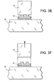
- figure 3E represents a component 21 carried on its final support 25, the component 21 being always integral with its support handle portion 10.
- figure 3F represents the component 21 fixed on its final support 25 and separated from its support handle portion 10.
- the separation can be performed by any mechanical or pneumatic means used alone or in combination.
- a variant of the method consists in cutting only the thin layer containing the elements to be transferred or only this layer and part of the handle. The removal of the element to be transferred is then simultaneous with the separation between the element and the support handle.
- a manipulator for example a vacuum micropipette
- a manipulator is used to postpone the element.
- the component can be separated from the support handle during the transfer. This is the case when a needle is used through a perforated support handle.
- the invention applies to the thinning of any type of semiconductor, for example silicon, germanium, III-V semiconductors (AsGa, InP, GaN). It also applies to the case where the plate is of any material but which can be thinned.
- the plate is planarized incompletely so as to clipping the summits of the relief and to obtain trays whose surface is about 2 mm 2 and whose roughness on this surface is less than 0.5 nm.
- This surface is for example silicon oxide or silicon nitride.
- the planarized surface represents 60% of the total area.
- the planarization is carried out by CMP and, after chemical cleaning, the plate is put in contact with its support handle which may be a surface-oxidized silicon plate or a glass plate possibly with a silicon oxide deposit on the surface. Annealing at 250 ° C. for two hours is carried out for this plate in order to obtain a bonding energy of the order of 600 mJ / m 2 . It is also possible to heat at a lower temperature and longer or vice versa to obtain a bonding energy of the same order of magnitude.
- the rear face of the plate containing the integrated circuits is thinned to a thickness of 10 microns, for example by rectification followed by chemical mechanical polishing.
- the circuits are then cut on their support handle using a standard saw.
- An alternative is to perform a deep etching of the thin layer carrying the components in a pattern such that it facilitates sawing, for example an engraving of the entire thin layer to a length greater than the kerf.
- a circuit can then be carried forward for example on a smart card by gluing the rear face of the circuit on the final support with an adhesive. Then, a pull is exerted so as to separate the front face of the circuit of the support handle.
- the rear face of the circuit is adhesively bonded to a wafer containing other circuits in order to produce 3D circuits.
- the securing of the rear face of the circuit can be done with a bonding energy of, for example, 1.5 J / m 2 . Such energy can be achieved through plasma cleaning.
- the intermediate support can be removed by introducing a blade to the bonding interface. A small recess may have been provided at the interface to facilitate insertion of the blade.
Landscapes
- Engineering & Computer Science (AREA)
- Manufacturing & Machinery (AREA)
- Microelectronics & Electronic Packaging (AREA)
- Mechanical Treatment Of Semiconductor (AREA)
- Element Separation (AREA)
- Micromachines (AREA)
- Recrystallisation Techniques (AREA)
- Led Devices (AREA)
- Container, Conveyance, Adherence, Positioning, Of Wafer (AREA)
- Bipolar Transistors (AREA)
- Formation Of Insulating Films (AREA)
Claims (12)
- Verfahren zur Gerinnung einer dünnen Schicht (23) aus einer Platte (20), enthaltend eine vordere Fläche, die in Oberflächenelemente unterteilt ist und die ein gegebenes Relief mit Erhebungen und eine rückwärtige Fläche zeigt, welches die Stufen umfasst, die bestehen aus:a) Bereitstellung eines Trägers (10), mit einer Fläche, die als Haftfläche dient;b) Herstellung der vorderen Fläche der Platte (20), wobei diese Herstellung die Einebnung des Reliefs als unvollständige Einebnung der vorderen Fläche der Platte umfasst, um, bezogen auf die Haftfläche des Trägers (10) eine Haftenergie Eo zu erhalten, die zwischen einem ersten Wert, welcher der minimalen Haftenergie, die mit dem anschließenden Schritt der Verdünnung verträglich ist, und einem zweiten Wert liegt, welcher der maximalen Haftenergie, die mit der anschließenden Operation der Aufweichung verträglich ist, entspricht, wobei die Haftenergie der Beziehung Eo=aE entspricht, wobei E die Haftenergie, die erhalten wird, wenn die vordere Fläche der Platte eingeebnet ist, und a das Verhältnis zwischen der unvollständig eingeebneten vorderen Fläche der Platte und der vollständig eingeebneten vorderen Fläche der Platte bedeutet und wobei a zwischen 0,4 und 0,8 liegt;c) Vereinigung der vorderen Fläche der Platte mit der Haftfläche (11) des Trägers (10) durch molekulare Haftung;d) Verdünnung der Platte (20), ausgehend von ihrer rückwärtigen Fläche, bis eine dünne Schicht (23) erhalten wird;e) Übertragung der Oberflächenelemente auf einen Gebrauchsträger, wobei die Trennung von dem Träger erfolgt.
- Verfahren nach Anspruch 1, dadurch gekennzeichnet, dass auf der Stufe e) die Gesamtheit der Oberflächenelemente auf den Gebrauchsträger übertragen wird.
- Verfahren nach Anspruch 1, dadurch gekennzeichnet, dass auf der Stufe e) das Verhältnis der Oberflächenelemente individuell gestaltet ist, die Stufe b) so ausgestaltet ist, dass für jedes Oberflächenelement eine Haftenergie E0 erhalten wird und der Stufe e) eine Stufe vorausgeht, auf der die dünnen Schicht in Oberflächenelemente zerschnitten wird.
- Verfahren nach Anspruch 1, dadurch gekennzeichnet, dass auf der Stufe e) das Verhältnis der Oberflächenelemente durch Gruppen von Oberflächenelementen dargestellt wird, die Stufe b) so ausgestaltet wird, dass für jede Gruppe von Oberflächenelementen eine Haftenergie Eo erhalten wird und der Stufe e) eine Stufe vorausgeht, auf der die dünne Schicht in eine Gruppe von Oberflächenelementen zerschnitten wird.
- Verfahren nach einem der Ansprüche 3 oder 4, dadurch gekenntzeichnet, dass das Zerschneiden der dünnen Schicht zusammen mit dem Zerschneiden des Trägers erfolgt.
- Verfahren nach einem der Ansprüche 3 bis 5, dadurch gekennzeichnet, dass die Stufe des Zerschneidens in Kombination mit einer Stufe der Tiefengravur der dünnen Schicht und einer Stufe des Sägens durchgeführt wird.
- Verfahren nach einem der Ansprüche 1 bis 6, dadurch gekennzeichnet, dass der Teil der Platte, der zur Bereitstellung der dünnen Schicht bestimmt ist, ein Halbleitermaterial darstellt.
- Verfahren nach Anspruch 7, dadurch gekennzeichnet, dass die Oberflächenelemente vollständige oder unvollständige elektronische Komponenten darstellen.
- Verfahren nach einem der Ansprüche 1 bis 8, dadurch gekennzeichnet, dass auf der Stufe b) die unvollständige Einebnung durch ein mechanisch-chemisches Polierverfahren durchgeführt wird.
- Verfahren nach einem der Ansprüche 1 bis 9, dadurch gekennzeichnet, dass auf der Stufe b) die Verdünnung der Platte durch ein mechanisches, chemisches oder mechanisch-chemisches Verdünnungsverfahren durchgeführt wird.
- Verfahren nach einem der Ansprüche 1 bis 10, dadurch gekennzeichnet, dass auf der Stufe e) die Entfernung vom Träger durch mechanische und/oder pneumatische Mittel durchgeführt wird.
- Verfahren nach einem der Ansprüche 1 bis 11, dadurch gekennzeichnet, dass auf der Stufe e) die Übertragung vor der Trennung vom Träger durchgeführt wird.
Applications Claiming Priority (3)
| Application Number | Priority Date | Filing Date | Title |
|---|---|---|---|
| FR0203909 | 2002-03-28 | ||
| FR0203909A FR2837981B1 (fr) | 2002-03-28 | 2002-03-28 | Procede de manipulation de couches semiconductrices pour leur amincissement |
| PCT/FR2003/000954 WO2003083930A1 (fr) | 2002-03-28 | 2003-03-26 | Procede de manipulation de couches semiconductrices pour leur amincissement |
Publications (2)
| Publication Number | Publication Date |
|---|---|
| EP1497857A1 EP1497857A1 (de) | 2005-01-19 |
| EP1497857B1 true EP1497857B1 (de) | 2010-05-19 |
Family
ID=27839282
Family Applications (1)
| Application Number | Title | Priority Date | Filing Date |
|---|---|---|---|
| EP03727614A Expired - Lifetime EP1497857B1 (de) | 2002-03-28 | 2003-03-26 | Verfahren zur manipulation von halbleiterschichten zum dünnmachen derselben |
Country Status (7)
| Country | Link |
|---|---|
| US (1) | US7205211B2 (de) |
| EP (1) | EP1497857B1 (de) |
| JP (1) | JP4593116B2 (de) |
| AT (1) | ATE468605T1 (de) |
| DE (1) | DE60332613D1 (de) |
| FR (1) | FR2837981B1 (de) |
| WO (1) | WO2003083930A1 (de) |
Families Citing this family (34)
| Publication number | Priority date | Publication date | Assignee | Title |
|---|---|---|---|---|
| FR2774511B1 (fr) * | 1998-01-30 | 2002-10-11 | Commissariat Energie Atomique | Substrat compliant en particulier pour un depot par hetero-epitaxie |
| FR2857502B1 (fr) | 2003-07-10 | 2006-02-24 | Soitec Silicon On Insulator | Substrats pour systemes contraints |
| FR2857983B1 (fr) * | 2003-07-24 | 2005-09-02 | Soitec Silicon On Insulator | Procede de fabrication d'une couche epitaxiee |
| FR2860842B1 (fr) * | 2003-10-14 | 2007-11-02 | Tracit Technologies | Procede de preparation et d'assemblage de substrats |
| DE10350036B4 (de) * | 2003-10-27 | 2014-01-23 | Robert Bosch Gmbh | Verfahren zum Vereinzeln von Halbleiterchips und entsprechende Halbleiterchipanordnung |
| DE102004010956B9 (de) | 2004-03-03 | 2010-08-05 | Infineon Technologies Ag | Halbleiterbauteil mit einem dünnen Halbleiterchip und einem steifen Verdrahtungssubstrat sowie Verfahren zur Herstellung und Weiterverarbeitung von dünnen Halbleiterchips |
| US7381950B2 (en) * | 2004-09-29 | 2008-06-03 | Texas Instruments Incorporated | Characterizing dimensions of structures via scanning probe microscopy |
| US7563691B2 (en) * | 2004-10-29 | 2009-07-21 | Hewlett-Packard Development Company, L.P. | Method for plasma enhanced bonding and bonded structures formed by plasma enhanced bonding |
| FR2878076B1 (fr) * | 2004-11-17 | 2007-02-23 | St Microelectronics Sa | Amincissement d'une plaquette semiconductrice |
| FR2879183B1 (fr) * | 2004-12-15 | 2007-04-27 | Atmel Grenoble Soc Par Actions | Procede de fabrication collective de microstructures a elements superposes |
| JP4349278B2 (ja) * | 2004-12-24 | 2009-10-21 | セイコーエプソン株式会社 | 半導体装置の製造方法 |
| CN100383929C (zh) * | 2005-02-01 | 2008-04-23 | 矽品精密工业股份有限公司 | 一种半导体处理制程 |
| US20070029043A1 (en) * | 2005-08-08 | 2007-02-08 | Silicon Genesis Corporation | Pre-made cleavable substrate method and structure of fabricating devices using one or more films provided by a layer transfer process |
| US20070032044A1 (en) * | 2005-08-08 | 2007-02-08 | Silicon Genesis Corporation | Method and structure for fabricating devices using one or more films provided by a layer transfer process and etch back |
| US7166520B1 (en) | 2005-08-08 | 2007-01-23 | Silicon Genesis Corporation | Thin handle substrate method and structure for fabricating devices using one or more films provided by a layer transfer process |
| DE102005048153B4 (de) * | 2005-10-06 | 2010-08-05 | Infineon Technologies Ag | Verfahren zur Herstellung eines Halbleiterbauteils mit Halbleiterchip und Klebstofffolie |
| FR2899594A1 (fr) | 2006-04-10 | 2007-10-12 | Commissariat Energie Atomique | Procede d'assemblage de substrats avec traitements thermiques a basses temperatures |
| US8124499B2 (en) * | 2006-11-06 | 2012-02-28 | Silicon Genesis Corporation | Method and structure for thick layer transfer using a linear accelerator |
| US20080128641A1 (en) * | 2006-11-08 | 2008-06-05 | Silicon Genesis Corporation | Apparatus and method for introducing particles using a radio frequency quadrupole linear accelerator for semiconductor materials |
| US20080188011A1 (en) * | 2007-01-26 | 2008-08-07 | Silicon Genesis Corporation | Apparatus and method of temperature conrol during cleaving processes of thick film materials |
| FR2919959B1 (fr) * | 2007-08-07 | 2009-12-18 | Commissariat Energie Atomique | Procede de transfert a basse temperature a partir d'une couche de molecules auto-assemblees |
| DE102008001738A1 (de) * | 2008-05-14 | 2009-11-26 | Robert Bosch Gmbh | Verfahren zur Herstellung von Chips |
| FR2936357B1 (fr) * | 2008-09-24 | 2010-12-10 | Commissariat Energie Atomique | Procede de report de puces sur un substrat. |
| FR2938117B1 (fr) | 2008-10-31 | 2011-04-15 | Commissariat Energie Atomique | Procede d'elaboration d'un substrat hybride ayant une couche continue electriquement isolante enterree |
| US7927975B2 (en) | 2009-02-04 | 2011-04-19 | Micron Technology, Inc. | Semiconductor material manufacture |
| FR2953065A1 (fr) * | 2009-11-20 | 2011-05-27 | Commissariat Energie Atomique | Procede de realisation d'empilements sur plusieurs niveaux d'ensembles de puces electroniques |
| SG177816A1 (en) * | 2010-07-15 | 2012-02-28 | Soitec Silicon On Insulator | Methods of forming bonded semiconductor structures, and semiconductor structures formed by such methods |
| US8481406B2 (en) | 2010-07-15 | 2013-07-09 | Soitec | Methods of forming bonded semiconductor structures |
| US8461017B2 (en) | 2010-07-19 | 2013-06-11 | Soitec | Methods of forming bonded semiconductor structures using a temporary carrier having a weakened ion implant region for subsequent separation along the weakened region |
| US9481566B2 (en) | 2012-07-31 | 2016-11-01 | Soitec | Methods of forming semiconductor structures including MEMS devices and integrated circuits on opposing sides of substrates, and related structures and devices |
| JPWO2014129433A1 (ja) | 2013-02-19 | 2017-02-02 | 日本碍子株式会社 | 複合基板及び半導体デバイスの製法 |
| US9248466B2 (en) | 2013-05-10 | 2016-02-02 | Infineon Technologies Ag | Application of fluids to substrates |
| JP6469070B2 (ja) * | 2016-12-21 | 2019-02-13 | エーファウ・グループ・エー・タルナー・ゲーエムベーハー | 第1の基板を第2の基板から剥離する方法および可撓性の基板保持装置の使用 |
| CN110838462B (zh) * | 2018-08-15 | 2022-12-13 | 北科天绘(合肥)激光技术有限公司 | 一种器件阵列的巨量转移方法及系统 |
Family Cites Families (16)
| Publication number | Priority date | Publication date | Assignee | Title |
|---|---|---|---|---|
| JP3287436B2 (ja) * | 1993-09-27 | 2002-06-04 | キヤノン株式会社 | 半導体装置の作製方法 |
| FR2725074B1 (fr) * | 1994-09-22 | 1996-12-20 | Commissariat Energie Atomique | Procede de fabrication d'une structure comportant une couche mince semi-conductrice sur un substrat |
| FR2748851B1 (fr) * | 1996-05-15 | 1998-08-07 | Commissariat Energie Atomique | Procede de realisation d'une couche mince de materiau semiconducteur |
| FR2767604B1 (fr) * | 1997-08-19 | 2000-12-01 | Commissariat Energie Atomique | Procede de traitement pour le collage moleculaire et le decollage de deux structures |
| FR2781925B1 (fr) * | 1998-07-30 | 2001-11-23 | Commissariat Energie Atomique | Transfert selectif d'elements d'un support vers un autre support |
| FR2796491B1 (fr) * | 1999-07-12 | 2001-08-31 | Commissariat Energie Atomique | Procede de decollement de deux elements et dispositif pour sa mise en oeuvre |
| FR2809867B1 (fr) * | 2000-05-30 | 2003-10-24 | Commissariat Energie Atomique | Substrat fragilise et procede de fabrication d'un tel substrat |
| US6303469B1 (en) * | 2000-06-07 | 2001-10-16 | Micron Technology, Inc. | Thin microelectronic substrates and methods of manufacture |
| FR2816445B1 (fr) * | 2000-11-06 | 2003-07-25 | Commissariat Energie Atomique | Procede de fabrication d'une structure empilee comprenant une couche mince adherant a un substrat cible |
| US7407869B2 (en) * | 2000-11-27 | 2008-08-05 | S.O.I.Tec Silicon On Insulator Technologies | Method for manufacturing a free-standing substrate made of monocrystalline semiconductor material |
| US6989314B2 (en) * | 2003-02-12 | 2006-01-24 | S.O.I.Tec Silicon On Insulator Technologies S.A. | Semiconductor structure and method of making same |
| JP2004319538A (ja) * | 2003-04-10 | 2004-11-11 | Seiko Epson Corp | 半導体装置の製造方法、集積回路、電子光学装置及び電子機器 |
| FR2857983B1 (fr) * | 2003-07-24 | 2005-09-02 | Soitec Silicon On Insulator | Procede de fabrication d'une couche epitaxiee |
| FR2867310B1 (fr) * | 2004-03-05 | 2006-05-26 | Soitec Silicon On Insulator | Technique d'amelioration de la qualite d'une couche mince prelevee |
| US20060014363A1 (en) * | 2004-03-05 | 2006-01-19 | Nicolas Daval | Thermal treatment of a semiconductor layer |
| CN101036222A (zh) * | 2004-09-21 | 2007-09-12 | S.O.I.Tec绝缘体上硅技术公司 | 通过实施共注入获得薄层的方法和随后的注入 |
-
2002
- 2002-03-28 FR FR0203909A patent/FR2837981B1/fr not_active Expired - Fee Related
-
2003
- 2003-03-26 DE DE60332613T patent/DE60332613D1/de not_active Expired - Lifetime
- 2003-03-26 US US10/509,007 patent/US7205211B2/en not_active Expired - Lifetime
- 2003-03-26 EP EP03727614A patent/EP1497857B1/de not_active Expired - Lifetime
- 2003-03-26 WO PCT/FR2003/000954 patent/WO2003083930A1/fr not_active Ceased
- 2003-03-26 AT AT03727614T patent/ATE468605T1/de not_active IP Right Cessation
- 2003-03-26 JP JP2003581250A patent/JP4593116B2/ja not_active Expired - Lifetime
Also Published As
| Publication number | Publication date |
|---|---|
| WO2003083930A1 (fr) | 2003-10-09 |
| FR2837981A1 (fr) | 2003-10-03 |
| FR2837981B1 (fr) | 2005-01-07 |
| JP4593116B2 (ja) | 2010-12-08 |
| US20050124138A1 (en) | 2005-06-09 |
| US7205211B2 (en) | 2007-04-17 |
| DE60332613D1 (de) | 2010-07-01 |
| JP2005528779A (ja) | 2005-09-22 |
| ATE468605T1 (de) | 2010-06-15 |
| EP1497857A1 (de) | 2005-01-19 |
Similar Documents
| Publication | Publication Date | Title |
|---|---|---|
| FR2837981A1 (fr) | Procede de manipulation de couches semiconductrices pour leur amincissement | |
| EP1378003B1 (de) | Verfahren zur herstellung eines abspaltbaren substrates oder einer abspaltbaren struktur | |
| EP1386346B1 (de) | Verfahren zum selektiven transferieren von halbleiter-chips von einem träger zu einem empfangssubstrat | |
| EP1299905B1 (de) | Verfahren zur trennung einer materialblocks und bildung eines dünnen films | |
| EP1378004B1 (de) | Methode zur herstellung eines abmontierbaren substrates mit kontrollierbarer mechanischen festigkeit | |
| EP0977252B1 (de) | Selektive Verlegung von Elementen von einem Träger zu einem anderen Träger | |
| EP1423873B1 (de) | Verfahren zum erhalten eines selbsttragenden halbleiterdünnfilms für elektronische schaltungen | |
| EP1923912B1 (de) | Verfahren zur Herstellung einer gemischten mikrotechnologischen Struktur | |
| EP1651560B1 (de) | Schichtstruktur und Herstellungsverfahren dafür | |
| EP1576658B1 (de) | Herstellungsverfahren für gemischte substrate und dadurch hergestellte struktur | |
| FR2880184A1 (fr) | Procede de detourage d'une structure obtenue par assemblage de deux plaques | |
| EP1364400B1 (de) | Herstellungsverfahren für dünne schichten auf einem spezifischen substrat und anwendung | |
| WO2015092254A1 (fr) | Procédé de fabrication d'un substrat-poignée destiné au collage temporaire d'un substrat | |
| FR2889887A1 (fr) | Procede de report d'une couche mince sur un support | |
| FR2938117A1 (fr) | Procede d'elaboration d'un substrat hybride ayant une couche continue electriquement isolante enterree | |
| EP2612352B1 (de) | Verfahren zur herstellung einer folie, etwa einer einkristallfolie, auf einem polymersubstrat | |
| FR2842651A1 (fr) | Procede de lissage du contour d'une couche utile de materiau reportee sur un substrat support | |
| EP1593152B1 (de) | Halbleitende struktur auf einem substrat mit starker rauheit | |
| WO2007006914A1 (fr) | Procede d'assemblage de substrats par depot d'une couche mince de collage d'oxyde ou de nitrure | |
| EP2676288B1 (de) | Verfahren zur herstellung einer substrathalterung | |
| FR3085230A1 (fr) | Separation d’une plaque en composants individuels. | |
| EP4668324A1 (de) | Verfahren zum direkten bonden von chips |
Legal Events
| Date | Code | Title | Description |
|---|---|---|---|
| PUAI | Public reference made under article 153(3) epc to a published international application that has entered the european phase |
Free format text: ORIGINAL CODE: 0009012 |
|
| 17P | Request for examination filed |
Effective date: 20040913 |
|
| AK | Designated contracting states |
Kind code of ref document: A1 Designated state(s): AT BE BG CH CY CZ DE DK EE ES FI FR GB GR HU IE IT LI LU MC NL PT RO SE SI SK TR |
|
| RIN1 | Information on inventor provided before grant (corrected) |
Inventor name: CLERC, JEAN-FREDERIC Inventor name: ASPAR, BERNARD Inventor name: ZUSSY, MARC |
|
| RAP1 | Party data changed (applicant data changed or rights of an application transferred) |
Owner name: COMMISSARIAT A L'ENERGIE ATOMIQUE |
|
| 17Q | First examination report despatched |
Effective date: 20080611 |
|
| GRAP | Despatch of communication of intention to grant a patent |
Free format text: ORIGINAL CODE: EPIDOSNIGR1 |
|
| GRAS | Grant fee paid |
Free format text: ORIGINAL CODE: EPIDOSNIGR3 |
|
| GRAA | (expected) grant |
Free format text: ORIGINAL CODE: 0009210 |
|
| RAP1 | Party data changed (applicant data changed or rights of an application transferred) |
Owner name: COMMISSARIAT A L'ENERGIE ATOMIQUE ET AUX ENERGIES |
|
| AK | Designated contracting states |
Kind code of ref document: B1 Designated state(s): AT BE BG CH CY CZ DE DK EE ES FI FR GB GR HU IE IT LI LU MC NL PT RO SE SI SK TR |
|
| REG | Reference to a national code |
Ref country code: GB Ref legal event code: FG4D Free format text: NOT ENGLISH |
|
| REG | Reference to a national code |
Ref country code: CH Ref legal event code: EP |
|
| REG | Reference to a national code |
Ref country code: IE Ref legal event code: FG4D Free format text: LANGUAGE OF EP DOCUMENT: FRENCH |
|
| REF | Corresponds to: |
Ref document number: 60332613 Country of ref document: DE Date of ref document: 20100701 Kind code of ref document: P |
|
| REG | Reference to a national code |
Ref country code: NL Ref legal event code: VDEP Effective date: 20100519 |
|
| PG25 | Lapsed in a contracting state [announced via postgrant information from national office to epo] |
Ref country code: SE Free format text: LAPSE BECAUSE OF FAILURE TO SUBMIT A TRANSLATION OF THE DESCRIPTION OR TO PAY THE FEE WITHIN THE PRESCRIBED TIME-LIMIT Effective date: 20100519 Ref country code: ES Free format text: LAPSE BECAUSE OF FAILURE TO SUBMIT A TRANSLATION OF THE DESCRIPTION OR TO PAY THE FEE WITHIN THE PRESCRIBED TIME-LIMIT Effective date: 20100830 |
|
| PG25 | Lapsed in a contracting state [announced via postgrant information from national office to epo] |
Ref country code: SI Free format text: LAPSE BECAUSE OF FAILURE TO SUBMIT A TRANSLATION OF THE DESCRIPTION OR TO PAY THE FEE WITHIN THE PRESCRIBED TIME-LIMIT Effective date: 20100519 Ref country code: FI Free format text: LAPSE BECAUSE OF FAILURE TO SUBMIT A TRANSLATION OF THE DESCRIPTION OR TO PAY THE FEE WITHIN THE PRESCRIBED TIME-LIMIT Effective date: 20100519 Ref country code: AT Free format text: LAPSE BECAUSE OF FAILURE TO SUBMIT A TRANSLATION OF THE DESCRIPTION OR TO PAY THE FEE WITHIN THE PRESCRIBED TIME-LIMIT Effective date: 20100519 |
|
| PG25 | Lapsed in a contracting state [announced via postgrant information from national office to epo] |
Ref country code: GR Free format text: LAPSE BECAUSE OF FAILURE TO SUBMIT A TRANSLATION OF THE DESCRIPTION OR TO PAY THE FEE WITHIN THE PRESCRIBED TIME-LIMIT Effective date: 20100820 Ref country code: CY Free format text: LAPSE BECAUSE OF FAILURE TO SUBMIT A TRANSLATION OF THE DESCRIPTION OR TO PAY THE FEE WITHIN THE PRESCRIBED TIME-LIMIT Effective date: 20100519 |
|
| REG | Reference to a national code |
Ref country code: IE Ref legal event code: FD4D |
|
| PG25 | Lapsed in a contracting state [announced via postgrant information from national office to epo] |
Ref country code: NL Free format text: LAPSE BECAUSE OF FAILURE TO SUBMIT A TRANSLATION OF THE DESCRIPTION OR TO PAY THE FEE WITHIN THE PRESCRIBED TIME-LIMIT Effective date: 20100519 Ref country code: PT Free format text: LAPSE BECAUSE OF FAILURE TO SUBMIT A TRANSLATION OF THE DESCRIPTION OR TO PAY THE FEE WITHIN THE PRESCRIBED TIME-LIMIT Effective date: 20100920 Ref country code: DK Free format text: LAPSE BECAUSE OF FAILURE TO SUBMIT A TRANSLATION OF THE DESCRIPTION OR TO PAY THE FEE WITHIN THE PRESCRIBED TIME-LIMIT Effective date: 20100519 Ref country code: EE Free format text: LAPSE BECAUSE OF FAILURE TO SUBMIT A TRANSLATION OF THE DESCRIPTION OR TO PAY THE FEE WITHIN THE PRESCRIBED TIME-LIMIT Effective date: 20100519 Ref country code: IE Free format text: LAPSE BECAUSE OF FAILURE TO SUBMIT A TRANSLATION OF THE DESCRIPTION OR TO PAY THE FEE WITHIN THE PRESCRIBED TIME-LIMIT Effective date: 20100519 |
|
| PG25 | Lapsed in a contracting state [announced via postgrant information from national office to epo] |
Ref country code: SK Free format text: LAPSE BECAUSE OF FAILURE TO SUBMIT A TRANSLATION OF THE DESCRIPTION OR TO PAY THE FEE WITHIN THE PRESCRIBED TIME-LIMIT Effective date: 20100519 Ref country code: CZ Free format text: LAPSE BECAUSE OF FAILURE TO SUBMIT A TRANSLATION OF THE DESCRIPTION OR TO PAY THE FEE WITHIN THE PRESCRIBED TIME-LIMIT Effective date: 20100519 Ref country code: RO Free format text: LAPSE BECAUSE OF FAILURE TO SUBMIT A TRANSLATION OF THE DESCRIPTION OR TO PAY THE FEE WITHIN THE PRESCRIBED TIME-LIMIT Effective date: 20100519 |
|
| PLBE | No opposition filed within time limit |
Free format text: ORIGINAL CODE: 0009261 |
|
| STAA | Information on the status of an ep patent application or granted ep patent |
Free format text: STATUS: NO OPPOSITION FILED WITHIN TIME LIMIT |
|
| 26N | No opposition filed |
Effective date: 20110222 |
|
| REG | Reference to a national code |
Ref country code: DE Ref legal event code: R097 Ref document number: 60332613 Country of ref document: DE Effective date: 20110221 |
|
| BERE | Be: lapsed |
Owner name: COMMISSARIAT A L'ENERGIE ATOMIQUE ET AUX ENERGIES Effective date: 20110331 |
|
| PG25 | Lapsed in a contracting state [announced via postgrant information from national office to epo] |
Ref country code: MC Free format text: LAPSE BECAUSE OF NON-PAYMENT OF DUE FEES Effective date: 20110331 |
|
| REG | Reference to a national code |
Ref country code: CH Ref legal event code: PL |
|
| PG25 | Lapsed in a contracting state [announced via postgrant information from national office to epo] |
Ref country code: BE Free format text: LAPSE BECAUSE OF NON-PAYMENT OF DUE FEES Effective date: 20110331 |
|
| PG25 | Lapsed in a contracting state [announced via postgrant information from national office to epo] |
Ref country code: LI Free format text: LAPSE BECAUSE OF NON-PAYMENT OF DUE FEES Effective date: 20110331 Ref country code: CH Free format text: LAPSE BECAUSE OF NON-PAYMENT OF DUE FEES Effective date: 20110331 |
|
| PG25 | Lapsed in a contracting state [announced via postgrant information from national office to epo] |
Ref country code: LU Free format text: LAPSE BECAUSE OF NON-PAYMENT OF DUE FEES Effective date: 20110326 |
|
| PG25 | Lapsed in a contracting state [announced via postgrant information from national office to epo] |
Ref country code: TR Free format text: LAPSE BECAUSE OF FAILURE TO SUBMIT A TRANSLATION OF THE DESCRIPTION OR TO PAY THE FEE WITHIN THE PRESCRIBED TIME-LIMIT Effective date: 20100519 Ref country code: BG Free format text: LAPSE BECAUSE OF FAILURE TO SUBMIT A TRANSLATION OF THE DESCRIPTION OR TO PAY THE FEE WITHIN THE PRESCRIBED TIME-LIMIT Effective date: 20100819 |
|
| PG25 | Lapsed in a contracting state [announced via postgrant information from national office to epo] |
Ref country code: HU Free format text: LAPSE BECAUSE OF FAILURE TO SUBMIT A TRANSLATION OF THE DESCRIPTION OR TO PAY THE FEE WITHIN THE PRESCRIBED TIME-LIMIT Effective date: 20100519 |
|
| REG | Reference to a national code |
Ref country code: FR Ref legal event code: PLFP Year of fee payment: 14 |
|
| REG | Reference to a national code |
Ref country code: FR Ref legal event code: PLFP Year of fee payment: 15 |
|
| REG | Reference to a national code |
Ref country code: FR Ref legal event code: PLFP Year of fee payment: 16 |
|
| PGFP | Annual fee paid to national office [announced via postgrant information from national office to epo] |
Ref country code: GB Payment date: 20220324 Year of fee payment: 20 Ref country code: DE Payment date: 20220322 Year of fee payment: 20 |
|
| PGFP | Annual fee paid to national office [announced via postgrant information from national office to epo] |
Ref country code: FR Payment date: 20220328 Year of fee payment: 20 |
|
| PGFP | Annual fee paid to national office [announced via postgrant information from national office to epo] |
Ref country code: IT Payment date: 20220331 Year of fee payment: 20 |
|
| REG | Reference to a national code |
Ref country code: DE Ref legal event code: R071 Ref document number: 60332613 Country of ref document: DE |
|
| REG | Reference to a national code |
Ref country code: GB Ref legal event code: PE20 Expiry date: 20230325 |
|
| PG25 | Lapsed in a contracting state [announced via postgrant information from national office to epo] |
Ref country code: GB Free format text: LAPSE BECAUSE OF EXPIRATION OF PROTECTION Effective date: 20230325 |