EP0977263A2 - Apparatus and method for reducing propagation delay in a conductor - Google Patents
Apparatus and method for reducing propagation delay in a conductor Download PDFInfo
- Publication number
- EP0977263A2 EP0977263A2 EP99305955A EP99305955A EP0977263A2 EP 0977263 A2 EP0977263 A2 EP 0977263A2 EP 99305955 A EP99305955 A EP 99305955A EP 99305955 A EP99305955 A EP 99305955A EP 0977263 A2 EP0977263 A2 EP 0977263A2
- Authority
- EP
- European Patent Office
- Prior art keywords
- conductor
- area
- conductive portion
- accordance
- along
- Prior art date
- Legal status (The legal status is an assumption and is not a legal conclusion. Google has not performed a legal analysis and makes no representation as to the accuracy of the status listed.)
- Withdrawn
Links
Images

Classifications
-
- H—ELECTRICITY
- H10—SEMICONDUCTOR DEVICES; ELECTRIC SOLID-STATE DEVICES NOT OTHERWISE PROVIDED FOR
- H10W—GENERIC PACKAGES, INTERCONNECTIONS, CONNECTORS OR OTHER CONSTRUCTIONAL DETAILS OF DEVICES COVERED BY CLASS H10
- H10W20/00—Interconnections in chips, wafers or substrates
- H10W20/40—Interconnections external to wafers or substrates, e.g. back-end-of-line [BEOL] metallisations or vias connecting to gate electrodes
- H10W20/41—Interconnections external to wafers or substrates, e.g. back-end-of-line [BEOL] metallisations or vias connecting to gate electrodes characterised by their conductive parts
- H10W20/423—Shielding layers
Definitions
- the present invention relates to electrical and integrated circuits and, in particular, to an electrical conductor for an electrical and/or integrated circuit.
- the transmission speed of an electrical signal along a conductor medium in an electrical circuit is dependent on several factors.
- the propagation delay of the pulse depends on the length of the medium and the wave velocity.
- the wave velocity is related to the dielectric constant of the surrounding medium and the speed of light.
- the RC time constant Another factor that delays the signal is caused by the resistance and capacitance of the conductor medium, commonly called the RC time constant.
- the speed of an electrical signal decreases when capacitance increases. Similarly, speed increases when capacitance decreases.
- the capacitance of the conductor medium depends on several factors, mainly the environment surrounding the conductor medium.
- an apparatus for decreasing the propagation delay time of an electrical signal transmitted along a conductor in a circuit includes a first conductor having a length extending from a first area of the circuit to a second area of the circuit and for carrying the electrical signal.
- a second conductor located proximate the first conductor extends substantially parallel and along the first conductor, with the second conductor electrically coupled to the first conductor.
- a conductor for transmitting a clocking signal from a first area to a second area of an integrated circuit.
- the conductor has a first elongated conductive portion extending from the first area to the second area and a second elongated conductive portion located proximate and spaced apart from the first conductive portion and extending substantially parallel with the first conductive portion.
- the conductor also includes a third elongated conductive portion located proximate and spaced apart from the first conductive portion and extending substantially parallel with the first conductive portion.
- the first conductive portion is electrically connected to the second conductive portion and the third conductive portion.
- a method of forming an electrical conductor in a circuit that increases the speed of an electrical signal transmitted along the conductor.
- the method includes the steps of fabricating a first conductor having a length extending from a first area of the circuit to a second area of the circuit, and fabricating a second conductor proximate the first conductor and extending substantially parallel and along the first conductor, the second conductor electrically coupled to the first conductor.
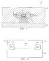
- FIGURE 1 there is shown a cross-sectional view of a medium ( semiconductor integrated circuit or printed circuit board, or the like) 8 having a substrate layer 20, an insulation layer 10, a first conductor 12 (also referenced as conductor A), a conductor 14 (also referenced as conductor D) and a conductor 16 (also referenced as conductor E) formed in the insulation layer 10.
- a medium 8 semiconductor integrated circuit or printed circuit board, or the like
- FIGURE 1 also shows capacitance paths 18 (illustrated in dotted lines) between the first conductor 12 and the conductors 14, 16.
- the substrate layer 20 which may include a conductive layer or other elements
- capacitance paths may exist between the conductor 12 and other elements or materials located proximate (above, beside, below) the conductor 12, but are not shown for convenience.
- a signal on one conductor increasing in voltage while a signal on another conductor decreases in voltage generates the maximum capacitive effect, while two signals increasing (or decreasing) together generates the least capacitive effect.
- the capacitive effect is great between non-shielded conductor lines when both signals are active and opposite in direction. This effect remains substantial when one signal is active (increasing or decreasing) and the other signal is static (e.g., one signal is rising to a logic one and the other signal is held at a logic zero).
- FIGURE 2 there is illustrated a circuit 100 having a conductor 120 extending from a first circuit 112 located in a first area 114 of an integrated circuit 100 to a second circuit 116 located in a second area 118 of the integrated circuit 100.
- the conductor 120 has a length L, as shown in FIGURE 2.
- the conductor 120 in accordance with the present invention reduces or decreases the propagation delay time (increases the speed) of an electrical signal transmitted along the conductor 120.
- the circuit 100 may also be any other electrical circuit, including a printed circuit board. Accordingly, the description of the present invention with respect to integrated circuits is also applicable to printed circuit boards and the like.
- the signal transmitted on the conductor 120 is a clocking signal and the propagation delay of the signal is reduced or decreased, thus increasing the speed of the signal.
- the length L of the conductor 120 should be more than about 250 microns, and preferably about 1000 microns or more. As will be appreciated, when used in an integrated circuit, the length L will most likely be less than 50,000 microns, depending on the size of the integrated circuit substrate.
- the signal(s) transmitted on the conductor 120 are generally about 10 MHz or greater and, preferably, about 200 MHz or greater, to obtain the many advantages of the present invention.
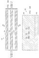
- the conductor 120 includes a first conductor 120a, a second conductor (or conductive portion) 120b extending substantially parallel and along the first conductor 120a, and a third conductor (or conductive portion) 120c extending substantially parallel and along the first conductor 120a.
- the conductors 120a, 120b, 120c are shown extending from the first circuit 112 (in the first area 114) to the second circuit 116 (in the second area 118) (see also FIGURE 2).
- Each of the conductors 120a, 120b, 120c are made of any conductive metal or material, preferably of low resistance, including copper, tungsten, aluminum, polysilicon or other material, or combination thereof.
- the additional conductor(s) may not run along the conductor 120a the entire distance L, but instead substantial portions may run along the conductor 120a.
- FIGURE 3B there is shown a cross-sectional view cut along line A-A of FIGURE 3A.
- the conductors 120a, 120b, 120c are formed in a insulating layer 200 (of an integrated circuit or printed circuit board, or the like). Additional layers of substrate may be provided, such as a substrate layer 202.
- the conductors 120b and 120c are each spaced apart substantially laterally from the conductor 120a, with the conductor 120b positioned along one side of the conductor 120a and the conductor 120c positioned along the other side of the conductor 120a.
- the width of each of the conductors is generally about 0.7 microns and the spacing therebetween is about 0.7 microns. However, the width and spacing dimensions may vary, and elements/dimensions in the figure may vary and may not be drawn to scale. It is expected that next generation processes will generate widths on the order of 0.2 to 0.4 microns, and perhaps even smaller.
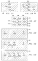
- FIGURES 4A-4C there are illustrated different configurations or embodiments for electrically connecting the conductors 120b, 120c to the main conductor 120a.
- the conductors 120a, 120b, 120c are electrically connected at or near the source end, as illustrated, using a conductive material, such as the material used to fabricate the conductors.
- a conductive material such as the material used to fabricate the conductors.
- source and destination are used for convenience and illustrative purposes only, and that the designations could be switched, such that the source end may refer to the first circuit 112 or first area 114, or the second circuit 116 or second area 118.
- the conductor 120 (or 120a) may be bi-directional, depending on the desired circuitry and functioning of the integrated circuit (or electrical circuit).
- FIGURE 4B there is illustrated another configuration or embodiment of the conductor 120 wherein the conductor 120a is electrically connected at one end to three separate drivers 210.
- Each driver 210 drives the respective conductors 120a, 120b, 120c.
- the drivers 210 may include any other type of circuitry, and are not limited to inverters.
- FIGURE 4C there is illustrated yet another configuration or embodiment of the conductor 120 wherein a plurality of switches 220 are used to electrically connect the conductor 120a to the conductor 120b, and to electrically connect the conductor 120a to the conductor 120c.
- the switches could also be tri-state devices. It will be understood to those skilled in the art that other circuits and methods may be used to electrically connect the conductor 120a to the conductors 120b, 120c.
- the conductors 120b and 120c could also be utilized by other circuitry when the conductor 120a is not active, unused, or when a signal is transmitted whose speed or propagation delay is unimportant. This is accomplished using switches and/or tri-state devices with appropriate control lines, and can be implemented by those skilled in the art.
- the conductor 120 includes a first conductor 120a, a second conductor (or conductive portion) 120b extending substantially parallel and along the first conductor 120a, and a third conductor (or conductive portion) 120c extending substantially parallel and along the first conductor 120a.
- the conductors 120b and 120c are each spaced apart substantially vertically from the conductor 120a, with the conductor 120b positioned along the top side of the conductor 120a and the conductor 120c positioned along the bottom side of the conductor 120a.
- the conductor 120 includes a first conductor 120a and a plurality of conductors (or conductive portions) 120b, 120c, 120d, 120e, whereby the conductors 120b, 120c, 120d, 120e each extend substantially parallel and along the first conductor 120a.
- the conductors 120b and 120c are each spaced apart substantially laterally from the conductor 120a, with the conductor 120b positioned along one side of the conductor 120a and the conductor 120c positioned along the other side of the conductor 120a.
- the conductors 120d and 120e are each spaced apart substantially vertically from the conductor 120a, with the conductor 120d positioned along the top side of the conductor 120a and the conductor 120e positioned along the bottom side of the conductor 120a.
- the conductor 120 in includes the conductors 120b, 120c, 120d, 120e as set forth in FIGURE 5B, and also includes a conductor 120f, a conductor 120g, a conductor 120h, and a conductor 120i, as shown in FIGURE 5C.
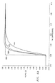
- FIGURES 6A-6D there are shown in FIGURE 6A signal waveforms in graphical representation illustrating rise times for a prior art conductor shown in FIGURE 6B, for one embodiment of the present invention shown in FIGURE 6C, and for another embodiment of the present invention shown in FIGURE 6D.
- FIGURE 6B there is shown the prior art conductor 12 with additional conductors 14 and 16.
- the width of each conductor 12, 14, 16 is about 0.7 microns and the spacing therebetween is about 2.1 microns.
- the conductors 14 and 16 are not electrically connected to the conductors 14 and 16.
- FIGURE 6C there is shown one embodiment of the present invention having the conductor 120 including the conductor 120a and 120b.
- the width of each conductor 120a, 120b, 14, 16 is about 0.7 microns and the spacing between the conductors 14, 120b and 120a is about 0.7 microns while the spacing between the conductors 120a and 16 is about 2.1 microns.
- the conductors 120a and 120b are electrically connected while the conductors 14 and 16 are not electrically connected to the conductor 120.
- FIGURE 6D there is shown one embodiment of the present invention having the conductor 120 including the conductor 120a and 120b.
- the width of each conductor 120a, 120b, 120c, 14, 16 is about 0.7 microns and the spacing therebetween is about 0.7 microns.
- the conductors 120a and 120b are electrically connected while the conductors 14 and 16 are not electrically connected to the conductor 120.
- FIGURE 6A there is shown a graph of voltage (volts) versus time (nanoseconds) comparing simulation results of the present invention with a prior art conductor.
- An ideal signal waveform for a signal transition from a logic zero (about 0 volts) to a logic one (about 3.3 volts) is identified by reference numeral 600, and illustrated with an instantaneous rise time.
- the waveform of a signal on the conductor 12 is identified by reference numeral 602, with the conductors 14 and 16 held at a logic zero.
- the prior art conductor 12 has a rise time (measured at about 90% of the logic one level of about 3.3 volts) of approximately 0.28 nanoseconds due to the capacitive effects of the conductors 14 and 16 on the conductor 12.
- the conductor 120a corresponds to the prior art conductor 12 shown in FIGURE 6B.
- the waveform of the signal on the conductor 120a is identified by reference numeral 604, with the conductors 14 and 16 held at a logic zero.
- the conductor 120a has a rise time of approximately 0.16 nanoseconds due to the capacitive effects of the conductors 14 and 16 on the conductor 12.
- the conductor 120a is "shielded" from some of the capacitive effects of the conductors 14 and 16 on the conductor 120a.
- the conductor 120 results in an increase in speed and decrease in rise time (with a corresponding decrease in propagation delay) of a signal transmitted on the conductor 120.
- the waveform of the signal on the conductor 120a is identified by reference numeral 606, with the conductors 14 and 16 held at a logic zero.
- the conductor 120a has a rise time of approximately 0.13 nanoseconds due to the capacitive effects of the conductors 14 and 16 on the conductor 12.
- the conductor 120a is "shielded" from some of the capacitive effects of the conductors 14 and 16 on the conductor 120a.
- the conductor 120 results in an increase in speed and decrease in rise time (with a corresponding decrease in propagation delay) of a signal transmitted on the conductor 120.
- the decrease/gain in rise time is about 0.15 nanoseconds. As shown, the decrease in rise time (increase in speed) is greater than a factor of two (and the corresponding reduction in propagation delay is greater than 50%).
- the signal on the conductors 120b and 120c will have slower rise time in voltage at the end of the conductor line than the conductor 120a. It will also be understood that the advantages of the present invention are also present for decreases in voltage (fall time) and not limited to increases in voltage (rise time).
- the capacitive effect (which causes delay) becomes greater as the dimensions of the integrated circuit (including printed circuit boards) decreases, and the next smaller generation of integrated circuits will incur a greater capacitive effect from line to line. Therefore, the present invention will be of increased benefit for future generation devices.
Landscapes
- Design And Manufacture Of Integrated Circuits (AREA)
- Semiconductor Integrated Circuits (AREA)
- Internal Circuitry In Semiconductor Integrated Circuit Devices (AREA)
Abstract
Description
Claims (17)
- An apparatus for decreasing the propagation delay time of an electrical signal transmitted along a conductor in a circuit, the apparatus comprising:a first conductor having a length extending from a first area of the circuit to a second area of the circuit and for carrying the electrical signal; anda second conductor located proximate the first conductor and extending substantially parallel and along the first conductor, the second conductor electrically coupled to the first conductor.
- The apparatus in accordance with Claim 1 further comprising a third conductor located proximate the first conductor and extending substantially parallel and along the first conductor, the third conductor electrically coupled to the first conductor.
- The apparatus in accordance with Claim 2 wherein the first conductor and the second conductor and the third conductor each comprise metal.
- The apparatus in accordance with Claim 2 further comprising a fourth conductor located proximate the first conductor and extending substantially parallel and along the first conductor, the fourth conductor electrically coupled to the first conductor.
- The apparatus in accordance with Claim 4 wherein the first conductor and the fourth conductor are located substantially in a second plane.
- The apparatus in accordance with Claim 1 wherein the second conductor reduces the effective capacitance of the first conductor thereby increasing the speed of the electrical signal transmitted on the first conductor.
- The apparatus in accordance with Claim 6 wherein the first conductor and the second conductor each comprise metal.
- An electrical conductor for increasing the speed of an electrical signal transmitted along the conductor in an integrated, the conductor comprising:a first conductor having a length extending from a first area of the integrated circuit to a second area of the integrated circuit;a second conductor located proximate the first conductor and extending substantially parallel and along the first conductor; andmeans for electrically coupling the first conductor to the second conductor.
- The electrical conductor in accordance with Claim 8 further comprising:a third conductor located proximate the first conductor and extending substantially parallel and along the first conductor; andmeans for electrically coupling the first conductor to the third conductor.
- The electrical conductor in accordance with Claim 1 or Claim 3 or Claim 9 conductor and the third conductor are located substantially in a same plane as the first conductor.
- The electrical conductor in accordance with Claim 9 wherein the coupling of the first conductor to the second conductor and to the third conductor decreases the effective capacitance of the first conductor thus decreasing the propagation delay time of the electrical signal transmitted along the first conductor from the first area to the second area of the integrated circuit.
- The electrical conductor in accordance with Claim 8 wherein the coupling of the first conductor to the second conductor decreases the effective capacitance of the first conductor thus decreasing the propagation delay time of the electrical signal transmitted along the first conductor from the first area to the second area of the integrated circuit.
- The electrical conductor in accordance with Claim 1 or Claim 12 wherein the length of the first conductor is greater tnan about 1000 microns.
- A conductor for transmitting a clocking signal from a first area to a second area of an integrated circuit, the conductor comprising:a first elongated conductive portion extending from the first area to the second area;a second elongated conductive portion located proximate and space apart from the first conductive portion and extending substantially parallel with the first conductive portion;a third elongated conductive portion located proximate and space apart from the first conductive portion and extending substantially parallel with the first conductive portion;means for electrically connecting the first conductive portion to the second conductive portion; andmeans for electrically connecting the first conductive portion to the third conductive portion.
- The conductor in accordance with Claim 14 wherein the second conductive portion and the third conductive portion reduce the capacitive effects on the first conductive portion thereby reducing the propagation delay of the clocking signal transmitted from the first area to the second area.
- The conductor in accordance with Claim 15 wherein the length of each of the first conductive portion, the second conductive portion, and the third conductive portion is greater than about 1000 microns.
- A method of forming an electrical conductor in a circuit for increasing the speed of an electrical signal transmitted along the conductor, comprising the steps of:fabricating a first conductor having a length extending from a first area of the circuit to a second area of the circuit; andfabricating a second conductor proximate the first conductor and extending substantially parallel and along the first conductor, such that when the first conductor and the second conductor are electrically coupled together while the electrical signal is transmitted along the first conductor from the first area to the second area, the propagation delay of the electrical signal is decreased.
Applications Claiming Priority (2)
| Application Number | Priority Date | Filing Date | Title |
|---|---|---|---|
| US12705098A | 1998-07-31 | 1998-07-31 | |
| US127050 | 1998-07-31 |
Publications (2)
| Publication Number | Publication Date |
|---|---|
| EP0977263A2 true EP0977263A2 (en) | 2000-02-02 |
| EP0977263A3 EP0977263A3 (en) | 2002-07-10 |
Family
ID=22428070
Family Applications (1)
| Application Number | Title | Priority Date | Filing Date |
|---|---|---|---|
| EP99305955A Withdrawn EP0977263A3 (en) | 1998-07-31 | 1999-07-27 | Apparatus and method for reducing propagation delay in a conductor |
Country Status (3)
| Country | Link |
|---|---|
| US (3) | US6842092B2 (en) |
| EP (1) | EP0977263A3 (en) |
| JP (1) | JP2000174017A (en) |
Cited By (1)
| Publication number | Priority date | Publication date | Assignee | Title |
|---|---|---|---|---|
| WO2002099970A1 (en) * | 2001-06-07 | 2002-12-12 | Koninklijke Philips Electronics N.V. | Controllable delay circuit for delaying an electric signal |
Families Citing this family (2)
| Publication number | Priority date | Publication date | Assignee | Title |
|---|---|---|---|---|
| EP0977263A3 (en) * | 1998-07-31 | 2002-07-10 | STMicroelectronics, Inc. | Apparatus and method for reducing propagation delay in a conductor |
| US8212634B2 (en) * | 2009-06-04 | 2012-07-03 | International Business Machines Corporation | Vertical coplanar waveguide with tunable characteristic impedance design structure and method of fabricating the same |
Family Cites Families (14)
| Publication number | Priority date | Publication date | Assignee | Title |
|---|---|---|---|---|
| JPS4921974B1 (en) * | 1969-06-30 | 1974-06-05 | ||
| US3659227A (en) * | 1970-09-08 | 1972-04-25 | Gen Electric | Switch-controlled directional coupler |
| JPS61119060A (en) * | 1984-11-14 | 1986-06-06 | Toshiba Corp | Signal propagation path for semiconductor integrated circuit |
| JPH0237763A (en) * | 1988-07-27 | 1990-02-07 | Nec Corp | Semiconductor integrated circuit |
| JP2736107B2 (en) * | 1989-03-14 | 1998-04-02 | 株式会社東芝 | Signal wiring board |
| US5043792A (en) * | 1989-04-17 | 1991-08-27 | Nec Corporation | Integrated circuit having wiring strips for propagating in-phase signals |
| JPH0473951A (en) * | 1990-07-16 | 1992-03-09 | Nec Ic Microcomput Syst Ltd | Semiconductor device |
| JPH04142074A (en) * | 1990-10-02 | 1992-05-15 | Seiko Epson Corp | Semiconductor device |
| JPH05136125A (en) * | 1991-11-14 | 1993-06-01 | Hitachi Ltd | Clock wiring and semiconductor integrated circuit device having clock wiring |
| DE69421591T2 (en) * | 1993-10-21 | 2000-06-08 | Advanced Micro Devices, Inc. | Dynamic high-density bus |
| JPH09237870A (en) * | 1996-03-01 | 1997-09-09 | Hitachi Ltd | Signal line drive |
| US5689217A (en) * | 1996-03-14 | 1997-11-18 | Motorola, Inc. | Directional coupler and method of forming same |
| US5742210A (en) * | 1997-02-12 | 1998-04-21 | Motorola Inc. | Narrow-band overcoupled directional coupler in multilayer package |
| EP0977263A3 (en) * | 1998-07-31 | 2002-07-10 | STMicroelectronics, Inc. | Apparatus and method for reducing propagation delay in a conductor |
-
1999
- 1999-07-27 EP EP99305955A patent/EP0977263A3/en not_active Withdrawn
- 1999-07-30 JP JP11216821A patent/JP2000174017A/en active Pending
-
2001
- 2001-01-09 US US09/757,378 patent/US6842092B2/en not_active Expired - Lifetime
-
2004
- 2004-11-23 US US10/997,089 patent/US7495526B2/en not_active Expired - Fee Related
-
2009
- 2009-02-11 US US12/378,073 patent/US20090206946A1/en not_active Abandoned
Cited By (1)
| Publication number | Priority date | Publication date | Assignee | Title |
|---|---|---|---|---|
| WO2002099970A1 (en) * | 2001-06-07 | 2002-12-12 | Koninklijke Philips Electronics N.V. | Controllable delay circuit for delaying an electric signal |
Also Published As
| Publication number | Publication date |
|---|---|
| US20050093640A1 (en) | 2005-05-05 |
| US7495526B2 (en) | 2009-02-24 |
| US6842092B2 (en) | 2005-01-11 |
| US20010018988A1 (en) | 2001-09-06 |
| US20090206946A1 (en) | 2009-08-20 |
| JP2000174017A (en) | 2000-06-23 |
| EP0977263A3 (en) | 2002-07-10 |
Similar Documents
| Publication | Publication Date | Title |
|---|---|---|
| US4514749A (en) | VLSI Chip with ground shielding | |
| US6281704B2 (en) | High-performance interconnect | |
| KR100283508B1 (en) | Non-solid reference plane with bidirectional impedance control | |
| US6937480B2 (en) | Printed wiring board | |
| US5194833A (en) | Airbridge compensated microwave conductors | |
| US5682124A (en) | Technique for increasing the range of impedances for circuit board transmission lines | |
| US20030107056A1 (en) | Substrate pads with reduced impedance mismatch and methods to fabricate substrate pads | |
| CN1102501A (en) | Electrical cable with improved shield | |
| US7759801B1 (en) | Tapered signal lines | |
| KR940012602A (en) | Semiconductor devices | |
| JPH10209580A (en) | Method and device for controlling signal line impedance of circuit board | |
| KR100394255B1 (en) | Wiring structure of semiconductor device | |
| US6242796B1 (en) | Wiring structure of semiconductor memory device and formation method thereof | |
| US20090206946A1 (en) | Apparatus and method for reducing propagation delay in a conductor | |
| US7170361B1 (en) | Method and apparatus of interposing voltage reference traces between signal traces in semiconductor devices | |
| EP0181600B1 (en) | Signal transmission circuit in a semiconductor integrated circuit | |
| WO2012039120A2 (en) | Printed circuit board | |
| US7309906B1 (en) | Apparatus and methods for providing highly effective and area efficient decoupling capacitance in programmable logic devices | |
| EP4060732B1 (en) | Shield structure for a low crosstalk single ended clock distribution circuit | |
| JPS61290794A (en) | Wiring board | |
| EP0837503A2 (en) | Reference plane metallization on an integrated circuit | |
| JP2017220505A (en) | Printed board | |
| JPH0691324B2 (en) | Wiring board | |
| JPH0669210A (en) | Integrated circuit | |
| JPH07135407A (en) | High frequency line |
Legal Events
| Date | Code | Title | Description |
|---|---|---|---|
| PUAI | Public reference made under article 153(3) epc to a published international application that has entered the european phase |
Free format text: ORIGINAL CODE: 0009012 |
|
| AK | Designated contracting states |
Kind code of ref document: A2 Designated state(s): AT BE CH CY DE DK ES FI FR GB GR IE IT LI LU MC NL PT SE |
|
| AX | Request for extension of the european patent |
Free format text: AL;LT;LV;MK;RO;SI |
|
| PUAL | Search report despatched |
Free format text: ORIGINAL CODE: 0009013 |
|
| AK | Designated contracting states |
Kind code of ref document: A3 Designated state(s): AT BE CH CY DE DK ES FI FR GB GR IE IT LI LU MC NL PT SE |
|
| AX | Request for extension of the european patent |
Free format text: AL;LT;LV;MK;RO;SI |
|
| 17P | Request for examination filed |
Effective date: 20030107 |
|
| AKX | Designation fees paid |
Designated state(s): DE FR GB IT |
|
| 17Q | First examination report despatched |
Effective date: 20051019 |
|
| STAA | Information on the status of an ep patent application or granted ep patent |
Free format text: STATUS: THE APPLICATION IS DEEMED TO BE WITHDRAWN |
|
| 18D | Application deemed to be withdrawn |
Effective date: 20070215 |