EP0977346A1 - Gleichstrom-Gleichstromwandler - Google Patents
Gleichstrom-Gleichstromwandler Download PDFInfo
- Publication number
- EP0977346A1 EP0977346A1 EP98870170A EP98870170A EP0977346A1 EP 0977346 A1 EP0977346 A1 EP 0977346A1 EP 98870170 A EP98870170 A EP 98870170A EP 98870170 A EP98870170 A EP 98870170A EP 0977346 A1 EP0977346 A1 EP 0977346A1
- Authority
- EP
- European Patent Office
- Prior art keywords
- capacitor
- current
- winding
- transformer
- switch
- Prior art date
- Legal status (The legal status is an assumption and is not a legal conclusion. Google has not performed a legal analysis and makes no representation as to the accuracy of the status listed.)
- Withdrawn
Links
Images





Classifications
-
- H—ELECTRICITY
- H02—GENERATION; CONVERSION OR DISTRIBUTION OF ELECTRIC POWER
- H02M—APPARATUS FOR CONVERSION BETWEEN AC AND AC, BETWEEN AC AND DC, OR BETWEEN DC AND DC, AND FOR USE WITH MAINS OR SIMILAR POWER SUPPLY SYSTEMS; CONVERSION OF DC OR AC INPUT POWER INTO SURGE OUTPUT POWER; CONTROL OR REGULATION THEREOF
- H02M3/00—Conversion of DC power input into DC power output
- H02M3/22—Conversion of DC power input into DC power output with intermediate conversion into AC
- H02M3/24—Conversion of DC power input into DC power output with intermediate conversion into AC by static converters
- H02M3/28—Conversion of DC power input into DC power output with intermediate conversion into AC by static converters using discharge tubes with control electrode or semiconductor devices with control electrode to produce the intermediate AC
- H02M3/325—Conversion of DC power input into DC power output with intermediate conversion into AC by static converters using discharge tubes with control electrode or semiconductor devices with control electrode to produce the intermediate AC using devices of a triode or a transistor type requiring continuous application of a control signal
- H02M3/335—Conversion of DC power input into DC power output with intermediate conversion into AC by static converters using discharge tubes with control electrode or semiconductor devices with control electrode to produce the intermediate AC using devices of a triode or a transistor type requiring continuous application of a control signal using semiconductor devices only
- H02M3/33538—Conversion of DC power input into DC power output with intermediate conversion into AC by static converters using discharge tubes with control electrode or semiconductor devices with control electrode to produce the intermediate AC using devices of a triode or a transistor type requiring continuous application of a control signal using semiconductor devices only of the forward type
Definitions
- the present invention relates to a circuit for DC / DC conversion with direct transfer.
- the present invention relates more particularly a new converter circuit to direct transfer called "forward converter”.
- converters In the field of DC / DC converters, there is known to use converters to transform a unipolar tension, preferably continuous, in one other unipolar voltage, preferably continuous, while guaranteeing galvanic isolation.
- a type of converter is called "forward" converter.
- Galvanic isolation consists of isolating the primary winding of the secondary winding of a transformer, hereinafter also called respectively primary and secondary, and allow to have a different potential across the secondary of that across the primary.
- the transformation ratio is the tension at the terminals of the secondary referred to the voltage at the terminals from primary.
- the "forward" converter presents as disadvantage of accumulating magnetization energy at level of the transformer core.
- winding tertiary or more simply tertiary, which returns this magnetization energy at the voltage source for the purpose to extract this magnetizing energy.
- forward converters several types can be distinguished, in particular the forward to a single switch, two switches or forward parallel.
- the forward to a single switch is the basis of the invention.
- the non-conduction phase is used to discharge the magnetized energy accumulated at the nucleus of the transformer while the conduction phase is used for conversion of the supply voltage.
- this behavior is characterized by a duty cycle (closing time on total period) less than or equal to 50%.
- the document EP-A-0474471 describes a DC voltage converter by signal switching rectangular under zero voltage, with one input for a DC voltage source, a transformer comprising a primary and connected to the first input, a main switch connected in series with the primary and the input of the DC voltage source as well as a clock signal generator to control the main switch.
- This converter includes a auxiliary switch and reversing capacitor magnetic connected in series with the primary and with the input of the DC voltage source, which auxiliary switch is controlled by the generator clock signal in phase opposition with respect to main switch and used to reset the transformer. It also includes means of switching delay.
- the present invention aims to obtain a improvement of the electronic circuit of the converter classic forward with a single switch, avoiding disadvantages of the state of the art.
- Another object of the present invention is to propose to make better use of electronic components which constitute the body of the electronic circuit and better distribute energy over all of said components.
- the present invention aims to increase the power density both per unit volume and weight only per unit cost of the various components.
- Another purpose complementary to this invention aims to recover energy from transformer leakage and magnetization inductors by part of the circuit during the phases of converter operation.
- Another purpose complementary to this invention aims to improve the dynamic behavior of the converter and increase its handling range.
- the present invention relates to a DC / DC converter controlled by a rectangular signal, having an input for a DC voltage source, a transformer with a primary winding connected at the DC voltage source and a winding secondary connected to the load, a single switch in series with the primary winding and the input of the source of DC voltage intended to carry out the signal rectangular, as well as a tertiary winding located at proximity of primary and secondary windings at level of the transformer core.
- the tertiary winding is in series with a diode on a branch arranged in parallel to the branch comprising the primary winding and the switch.
- the tertiary winding disposed at the level of the transformer has the same winding direction as primary winding.
- Tertiary winding may be weak coupled, possibly wound on a separate core.
- the converter includes components electronic to build a first circuit current flow to drain energy at least contained in the leakage inductance and in the inductance of magnetization of the transformer, and a second circuit of current flow to return this energy accumulated as a magnetization induction reversed to the transformer.
- an inversion capacitor magnetic allowing the reset of the transformer is provided, preferably placed between the branch comprising the primary winding and the switch and the panel including the tertiary winding and the diode, as well that a second diode having the blocking direction vis-à-vis of the DC voltage source in series with tertiary winding.
- the first current circulation circuit therefore includes the primary winding, the capacitor, the first diode intended to form a circulation loop of current through which a current of the primary winding towards the capacitor allowing to accumulate at least the leakage inductance energy and magnetization of the transformer.
- the second current circulation circuit includes the primary winding, the capacitor, the second diode and the tertiary winding to form a current circulation loop with voltage source input of the converter through which a current from the capacitor to the primary winding for return the energy accumulated at the level of the capacitor to the transformer in the form of an induction of reverse magnetization.
- the converter according to the present invention thus exhibits dynamic behavior and energy behavior improved by the positioning of the tertiary winding in the same direction winding that the primary and secondary transformer, and by adding only two additional components which are a capacitor and a second diode.
- the type of converter behavior is mainly determined by the choice of these two elements and their arrangement in the circuit to lead to the formation of the two current circulation circuits previously mentioned.
- the realization of a rectangular signal of the voltage source is obtained by placing the switch cyclically in a conduction phase and in a non-conduction phase.
- This signal switching rectangular can in particular be performed at frequency constant by means of a conventional regulation circuit.
- the regulation circuit is used to give a low electrical potential control signal in order to place the transistor in phase passing or in situation of conduction.
- the circuit of the converter first absorbs the energy contained in transformer level by means of a loop current flow including the primary winding of the transformer, the capacitor and the first diode.
- the direction of flow in this loop is determined by the first diode which will only be conducting for a current of circulation from the primary winding to the capacitor.
- the circuit of the converter returns the energy stored at the capacitor in the form of a magnetization induction reverse to the transformer core, using a second current circulation circuit comprising series the primary winding, the capacitor, the second diode and tertiary winding. These elements forming a loop with the input voltage source of the converter.
- the direction of circulation in this loop is determined by the second diode which will only be on for circulation current from the winding tertiary to the capacitor and from the capacitor to primary winding.
- the energy stored at the level of capacitor is transferred via the primary windings and tertiary in the form of a magnetization induction reverse to the transformer core.
- An additional feature of the present invention relates to the fact that the current of magnetization through the transformer which, by the fact to be inverted when the energy stored in the circuit at the transformer core, takes a shape bipolar almost symmetrical with respect to the value 0 of complete demagnetization of the transformer core.
- the core of the transformer undergoes a following positive and negative magnetization induction a balanced distribution in relation to the situation completely demagnetized.
- Another particular advantage of this The invention relates to the conduction period of the switch.
- Another advantage of the present invention lies in soft switching of the switch by excluding sudden variations in voltage across the switch.
- the switch cuts off the flow of current from the source of input voltage to the primary winding.
- the current flow at the secondary level is not canceled however and the secondary winding continues to be traversed by a current which, ultimately, is reflected on the primary winding.
- the converter electronics according to this invention provides that the flow of the current image secondary is carried out through the capacitor in the first circulation circuit.
- the first diode and the capacitor realize a switching assistance circuit also called non-dissipative snubber, which allows the switch to open at zero voltage and soft switching.
- Another advantage of the converter according to the present invention lies in the fact that the maximum voltage across the terminals of the switch S remains constant. Indeed, the maximum voltage at the terminals of switch S is both proportional to the input voltage (V DC ) and to the duty cycle (D). The maximum stress is therefore proportional to the product V DC x D, ie the output voltage, often regulated and therefore constant.
- the Duty-cycle D can take a value greater than 50%, a wide range of values is obtained.
- the supply voltage V DC at the input of the converter can easily be chosen in a range going from simple to double and which, for example, is between 40 and 80 volts and even more, without resorting to the use of larger or larger items of value for the transformer core and the switch.
- the duty cycle can therefore be chosen in a range of 0 to 100%.
- the converter according to this invention especially exhibits dynamic behavior flexible, especially when changing from a stationary operation to another situation of stationary operation by simple variation of the duty cycle or input voltage or whatever. Converter then quickly finds a system without runaway steady state.
- the converter according to this overall has fewer components electronic than those already known.
- a third diode is planned in parallel on the tertiary winding and the second diode of the second traffic circuit.
- the electronic diagram can be subdivided into two circuits including the input circuit comprising the primary and tertiary winding of the transformer and the output circuit comprising the secondary winding of the transformer.
- the output circuit acts as a filter output and includes electronic components following: a DS1 diode, an L coil, in series with secondary winding 2 and a DS2 diode, a capacitor CS and a load RL in parallel with the secondary winding.
- the DS2 diode and the capacitor being arranged on either side of the coil L.
- the input circuit serves as a conduction, demagnetization and restoration circuit for the converter. It includes the DC voltage source symbolized by V DC which constitutes the energy and supply source of the converter. At the terminals of the voltage source there is in series the primary winding 1 of the transformer with the switch S.
- the input circuit can be subdivided into two current circulation circuits, in particular a first current circulation circuit and a second current circulation circuit.
- the first current circulation circuit is a loop formed by the primary winding 1, the capacitor C and diode D1.
- the passing direction of the diode D1 alone allows a flow of current from primary winding 1 to capacitor C.
- the second current circulation circuit comprises at the terminals of the voltage source V DC the primary winding 1 in series with the capacitor C, the diode D2 and the tertiary winding 3.
- the passing direction of the diode D2 alone allows circulation from the current from the tertiary winding 3 to the capacitor C and from the capacitor C to the primary winding 1 of the transformer.
- the primary windings 1, secondary 2 and tertiary 3 are polarized in the same direction and the number of turns n3 of the tertiary winding 3 is at most equal to the number of turns n1 of the winding primary.
- the energy is drawn from the voltage source V DC via the primary winding 1 and secondary 2 of the transformer and is transmitted directly to the filter. Release.
- the path of the current taken in the input circuit is from the voltage source V DC to the primary winding 1, then via the switch S in the closed position to the voltage source V DC to close the circulation loop.
- the current flows in the direction passing from the DS1 diode through the coil L to supply an output load symbolized by RL.
- Switching to the closed position of the switch S induces a current flow of the tertiary winding through diodes D2 and D1 and allows to restore the initial conditions of tension to capacitor terminals.
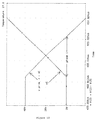
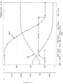
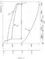
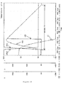
- FIGs 2 to 8 show diagrams diagrams of converter operation according to the invention. How the converter works the invention can be divided into seven phases. These different phases are designated by phases 0 to 6 and are described in Figures 9 to 15.
- Phase 0 constitutes the phase of converter operation when the switch is closed, i.e. in conduction state.
- Phases 1 to 6 constitute the phases of converter operation since switching the conduction state to the non-conduction state of the switch until switching of non-conduction state in the conduction state of the switch.
- Phase 0 Energy transfer phase from source V DC to the load RL through the transformer
- the energy transfer induces an increase in the current i O through the coil L.
- the magnetization current i M there is also a linear increase in the magnetization current i M at the level of the transformer core.
- the magnetization inductance of the transformer stores energy from the source V DC .
- Phase 1 Secondary current transfer phase
- the switch opens and goes from the conduction state to the non-conduction state.
- the image of the secondary current is reflected on the primary winding and charges the capacitor C by increasing the voltage V C across its terminals.
- the capacitor C slows the growth of the voltage V S at the terminals of the switch S which can then open by soft switching.
- This phase ends when the voltage V 1 , at the terminals of the transformer, that is to say of the primary winding is canceled.
- Phase 2 Leakage induction transfer phase
- This phase ends when the circulation current i DS1 through the diode DS1 is canceled.
- Phase 3 Induction transfer phase magnetization
- Phase 4 Transfer of energy stored in the internal capacity of the switch to the transformer
- the internal capacity Cp at switch S resonates with the inductance of magnetization, which induces a current from the capacitor internal Cp of the switch to the primary winding of the transformer.
- This phase ends when the difference potential across D2 is such that this enters in the conduction phase, that is to say in a busy situation.
- the diode D2 enters conduction so that the two primary windings and of the transformer are found in series with the capacitor C.
- this step is characterized by the on state of the diode D2. Following the passage of the current through the capacitor C, which discharges through the primary, a voltage drop V C is observed at the terminals of the capacitor C and a growth of the reverse magnetization induction i M at the transformer in addition negative.
- This phase is also characterized by a voltage drop V S at the terminals of the switch S and of the primary and tertiary windings (cf. FIG. 7).
- the restoration step is characterized by the passage of a large current i D2 , i D1 respectively through the diodes D2 and D1, thus allowing a voltage drop V C from V DC to -V DC .
- this phase is characterized by a current i DS1 in the diode DS1 which begins to increase.
- the current i DS1 reaches the value i 0 through the coil, the current i DS2 through the diode DS2 is interrupted (see Figure 8).
- Figures 16 and 17 show two more embodiments of the DC / DC conversion circuit according to the present invention, in which it is desired to improve the characteristics of the circuit making it possible to obtain a Duty-cycle even higher than that obtained using the device of Figure 1 without increasing the voltage constraints on switch S.
- an additional winding 4 is added to the transformer to allow phase 5 to start earlier and to obtain an even faster evolution of the voltage across the capacitor C thanks to an even lower transformer impedance.
- the equivalent magnetization impedance of the transformer seen by the circuit must be multiplied by (1 - m) 2 if m is the factor of the additional winding 4 of the transformer (compared to the primary winding).
- diode D3 and winding 4 carry a very weak current, this which means they can be relatively small size compared to other elements. This reduces obviously their cost.
- phase 5 the course of the current through diode D2 and winding 3 is replaced by a path through diode D3 (see figure 16) and possibly winding 4 (see Figure 17).
- V S V DC (1 + 1 / m) .
- winding 4 will serve as an absolute field for the voltage applied to switch S.
Landscapes
- Engineering & Computer Science (AREA)
- Power Engineering (AREA)
- Dc-Dc Converters (AREA)
- Amplifiers (AREA)
- Details Of Television Scanning (AREA)
Priority Applications (7)
| Application Number | Priority Date | Filing Date | Title |
|---|---|---|---|
| EP98870170A EP0977346A1 (de) | 1998-07-31 | 1998-07-31 | Gleichstrom-Gleichstromwandler |
| AT99936192T ATE429066T1 (de) | 1998-07-31 | 1999-07-27 | Gleichstrom-gleichstromwandlerschaltung |
| EP99936192A EP1101276B1 (de) | 1998-07-31 | 1999-07-27 | Gleichstrom-gleichstromwandlerschaltung |
| US09/762,150 US6421255B1 (en) | 1998-07-31 | 1999-07-27 | DC-to-DC converting circuit |
| AU51423/99A AU5142399A (en) | 1998-07-31 | 1999-07-27 | Dc-to-dc converting circuit |
| DE69940739T DE69940739D1 (de) | 1998-07-31 | 1999-07-27 | Gleichstrom-gleichstromwandlerschaltung |
| PCT/BE1999/000095 WO2000008741A1 (fr) | 1998-07-31 | 1999-07-27 | Circuit de conversion dc/dc |
Applications Claiming Priority (1)
| Application Number | Priority Date | Filing Date | Title |
|---|---|---|---|
| EP98870170A EP0977346A1 (de) | 1998-07-31 | 1998-07-31 | Gleichstrom-Gleichstromwandler |
Publications (1)
| Publication Number | Publication Date |
|---|---|
| EP0977346A1 true EP0977346A1 (de) | 2000-02-02 |
Family
ID=8237077
Family Applications (2)
| Application Number | Title | Priority Date | Filing Date |
|---|---|---|---|
| EP98870170A Withdrawn EP0977346A1 (de) | 1998-07-31 | 1998-07-31 | Gleichstrom-Gleichstromwandler |
| EP99936192A Expired - Lifetime EP1101276B1 (de) | 1998-07-31 | 1999-07-27 | Gleichstrom-gleichstromwandlerschaltung |
Family Applications After (1)
| Application Number | Title | Priority Date | Filing Date |
|---|---|---|---|
| EP99936192A Expired - Lifetime EP1101276B1 (de) | 1998-07-31 | 1999-07-27 | Gleichstrom-gleichstromwandlerschaltung |
Country Status (6)
| Country | Link |
|---|---|
| US (1) | US6421255B1 (de) |
| EP (2) | EP0977346A1 (de) |
| AT (1) | ATE429066T1 (de) |
| AU (1) | AU5142399A (de) |
| DE (1) | DE69940739D1 (de) |
| WO (1) | WO2000008741A1 (de) |
Cited By (4)
| Publication number | Priority date | Publication date | Assignee | Title |
|---|---|---|---|---|
| EP1806832A1 (de) | 2006-01-10 | 2007-07-11 | Samsung Electronics Co., Ltd. | DC-DC-Wandler |
| FR2959892A1 (fr) * | 2010-05-06 | 2011-11-11 | Sagem Defense Securite | Convertisseur a decoupage disposant d'un circuit d'aide a la commutation |
| EP2757673A3 (de) * | 2013-01-22 | 2016-02-17 | TDK-Lambda UK Limited | Wandler |
| US9780642B2 (en) | 2014-02-24 | 2017-10-03 | Tdk-Lambda Uk Limited | Energy recovery snubber |
Families Citing this family (12)
| Publication number | Priority date | Publication date | Assignee | Title |
|---|---|---|---|---|
| US6314002B1 (en) * | 2000-11-20 | 2001-11-06 | Philips Electronics North America Corporation | Voltage clamping system and method for a DC/DC power converter |
| US6473318B1 (en) * | 2000-11-20 | 2002-10-29 | Koninklijke Philips Electronics N.V. | Leakage energy recovering system and method for flyback converter |
| US7385833B2 (en) * | 2005-06-03 | 2008-06-10 | Astec International Limited | Snubber circuit for a power converter |
| US20080304299A1 (en) * | 2006-09-11 | 2008-12-11 | Bormann Ronald M | Low voltage LED drive from 120VAC line |
| US8000112B2 (en) * | 2008-04-11 | 2011-08-16 | Flextronics Ap, Llc | Active snubber for transition mode power converter |
| US20090257254A1 (en) * | 2008-04-15 | 2009-10-15 | National Taiwan University Of Science And Technology | Voltage-clamp power converters |
| TWI389438B (zh) * | 2009-11-02 | 2013-03-11 | Analog Integrations Corp | 高轉換效率之電壓轉換器 |
| US9379659B2 (en) | 2010-11-08 | 2016-06-28 | Regal Beloit America, Inc. | Lossless snubber drive for a permanent magnet synchronous motor |
| TWI732581B (zh) * | 2020-06-03 | 2021-07-01 | 亞源科技股份有限公司 | 具減震控制之轉換裝置及其減震控制的操作方法 |
| CN112072922B (zh) * | 2020-09-01 | 2022-11-25 | 亚瑞源科技(深圳)有限公司 | 一种具减震控制之转换装置及其减震控制的操作方法 |
| JP7676212B2 (ja) * | 2021-04-30 | 2025-05-14 | キヤノン株式会社 | 電源装置及び画像形成装置 |
| JP7767113B2 (ja) * | 2021-11-02 | 2025-11-11 | キヤノン株式会社 | 電源装置及び画像形成装置 |
Citations (2)
| Publication number | Priority date | Publication date | Assignee | Title |
|---|---|---|---|---|
| US4268898A (en) * | 1980-03-20 | 1981-05-19 | Lorain Products Corporation | Semiconductor switching circuit with clamping and energy recovery features |
| DE3634990A1 (de) * | 1985-11-28 | 1987-06-04 | Schrack Elektronik Ag | Verlustarmes spannungsbegrenzungsnetzwerk fuer sperr- oder flusswandler |
Family Cites Families (3)
| Publication number | Priority date | Publication date | Assignee | Title |
|---|---|---|---|---|
| US5331534A (en) * | 1991-11-20 | 1994-07-19 | Tokyo Electric Co., Ltd. | Power supply apparatus |
| US5523936A (en) * | 1994-07-25 | 1996-06-04 | Chun-Shan Institute Of Science And Technology | Built-in input filter forward converter |
| US5883795A (en) * | 1998-04-28 | 1999-03-16 | Lucent Technologies Inc. | Clamp circuit for a power converter and method of operation thereof |
-
1998
- 1998-07-31 EP EP98870170A patent/EP0977346A1/de not_active Withdrawn
-
1999
- 1999-07-27 DE DE69940739T patent/DE69940739D1/de not_active Expired - Lifetime
- 1999-07-27 EP EP99936192A patent/EP1101276B1/de not_active Expired - Lifetime
- 1999-07-27 US US09/762,150 patent/US6421255B1/en not_active Expired - Lifetime
- 1999-07-27 AT AT99936192T patent/ATE429066T1/de not_active IP Right Cessation
- 1999-07-27 WO PCT/BE1999/000095 patent/WO2000008741A1/fr not_active Ceased
- 1999-07-27 AU AU51423/99A patent/AU5142399A/en not_active Abandoned
Patent Citations (2)
| Publication number | Priority date | Publication date | Assignee | Title |
|---|---|---|---|---|
| US4268898A (en) * | 1980-03-20 | 1981-05-19 | Lorain Products Corporation | Semiconductor switching circuit with clamping and energy recovery features |
| DE3634990A1 (de) * | 1985-11-28 | 1987-06-04 | Schrack Elektronik Ag | Verlustarmes spannungsbegrenzungsnetzwerk fuer sperr- oder flusswandler |
Non-Patent Citations (1)
| Title |
|---|
| VARGA L D ET AL: "A NOVEL LOSSLESS SNUBBER CIRCUIT", PROCEEDINGS OF THE ANNUAL APPLIED POWER ELECTRONICS CONFERENCE AND EXPOSITION. (APEC), BALTIMORE, MAR. 13 - 17, 1989, no. CONF. 4, 13 March 1989 (1989-03-13), INSTITUTE OF ELECTRICAL AND ELECTRONICS ENGINEERS, pages 40 - 45, XP000044248 * |
Cited By (6)
| Publication number | Priority date | Publication date | Assignee | Title |
|---|---|---|---|---|
| EP1806832A1 (de) | 2006-01-10 | 2007-07-11 | Samsung Electronics Co., Ltd. | DC-DC-Wandler |
| US7630219B2 (en) | 2006-01-10 | 2009-12-08 | Samsung Electronics Co., Ltd. | DC to DC converter for decreasing switching loss according to the turn-on/turn-off state of a switch |
| FR2959892A1 (fr) * | 2010-05-06 | 2011-11-11 | Sagem Defense Securite | Convertisseur a decoupage disposant d'un circuit d'aide a la commutation |
| EP2757673A3 (de) * | 2013-01-22 | 2016-02-17 | TDK-Lambda UK Limited | Wandler |
| US9362831B2 (en) | 2013-01-22 | 2016-06-07 | Tdk-Lambda Uk Limited | Fly-forward converter with energy recovery snubber |
| US9780642B2 (en) | 2014-02-24 | 2017-10-03 | Tdk-Lambda Uk Limited | Energy recovery snubber |
Also Published As
| Publication number | Publication date |
|---|---|
| EP1101276A1 (de) | 2001-05-23 |
| US6421255B1 (en) | 2002-07-16 |
| EP1101276B1 (de) | 2009-04-15 |
| AU5142399A (en) | 2000-02-28 |
| DE69940739D1 (de) | 2009-05-28 |
| WO2000008741A1 (fr) | 2000-02-17 |
| ATE429066T1 (de) | 2009-05-15 |
Similar Documents
| Publication | Publication Date | Title |
|---|---|---|
| EP1101276B1 (de) | Gleichstrom-gleichstromwandlerschaltung | |
| EP0722211B1 (de) | Bidirektionaler Gleichstrom-Gleichstrom-Spannungswandler und Stromsensor | |
| EP0722212B1 (de) | Bidirektionale Gleichstrom-Gleichstrom-Spannungswandler und Stromsensor | |
| EP0737989A1 (de) | Schaltnetzteil mit einem sättigbaren Induktor zur Gestaltung einer Pulsstromquelle | |
| WO2002073783A2 (fr) | Circuit d'aide a la commutation d'un convertisseur a decoupage | |
| EP0803067A1 (de) | Bidirektionaler gleichspannung-gleichspannung-umformer und stromwandler | |
| EP2882087A1 (de) | Gleichstrom-Gleichstrom-Wandler in diskontinuierlichem Betriebsmodus | |
| EP2320553B1 (de) | Stromumwandlungsvorrichtung und unterbrechungsfreie Stromversorgung, die eine solche Vorrichtung umfasst | |
| FR2627644A1 (fr) | Convertisseur continu-continu, sans pertes de commutation, notamment pour alimentation continue haute frequence ou pour amplificateur a tube a ondes progressives | |
| FR2712126A1 (fr) | Amplificateur de puissance du type pont en H et ses moyens de blocage et dispositif amplificateur de puissance comportant de tels amplificateurs. | |
| FR2477338A1 (fr) | Circuit de sortie empeche de se bloquer du fait d'impulsions de tension produites par une charge inductive | |
| EP3945674A1 (de) | Spannungswandler | |
| EP1986314B1 (de) | Steuerverfahren eines Schaltnetzteils mit einem einzigen induktiven Element und mehreren Ausgängen, sowie entsprechende Schaltnetzteilvorrichtung, insbesondere für ein Mobiltelefon | |
| FR2802359A1 (fr) | Circuit d'alimentation pour moteur piezo-electrique | |
| EP1953904A1 (de) | Dämpferschaltung für einen Schaltkonverter | |
| FR2717015A1 (fr) | Alimentation à découpage adaptée pour permettre des commutations sous tension réduite. | |
| EP2286508A1 (de) | Überspannungsbegrenzung in einem chopping-wandler | |
| EP3584918B1 (de) | Schaltwandler | |
| EP0184493B1 (de) | Gleichstromregler mit Taktschalter und Transformator | |
| EP3195459B1 (de) | Gleichspannungswandler und zugehöriges steuerungsverfahren | |
| EP1929630A1 (de) | Strikte steuerung elektrischer stromumsetzer | |
| FR2744857A1 (fr) | Convertisseur d'energie electrique a inverseurs resonants "demi-periode" | |
| EP0195713A1 (de) | Kommutierungshilfseinrichtung für Schalter und Freilaufdiode | |
| EP0928057A1 (de) | Hochspannungsschalter aus reihengeschalteten resonanten Zellen | |
| FR2707053A1 (en) | Voltage converter of the inverter type for supplying an electric load, especially a fluorescent tube |
Legal Events
| Date | Code | Title | Description |
|---|---|---|---|
| PUAI | Public reference made under article 153(3) epc to a published international application that has entered the european phase |
Free format text: ORIGINAL CODE: 0009012 |
|
| AK | Designated contracting states |
Kind code of ref document: A1 Designated state(s): AT BE CH CY DE DK ES FI FR GB GR IE IT LI LU MC NL PT SE |
|
| AX | Request for extension of the european patent |
Free format text: AL;LT;LV;MK;RO;SI |
|
| AKX | Designation fees paid | ||
| STAA | Information on the status of an ep patent application or granted ep patent |
Free format text: STATUS: THE APPLICATION IS DEEMED TO BE WITHDRAWN |
|
| 18D | Application deemed to be withdrawn |
Effective date: 20000803 |