EP1986314B1 - Steuerverfahren eines Schaltnetzteils mit einem einzigen induktiven Element und mehreren Ausgängen, sowie entsprechende Schaltnetzteilvorrichtung, insbesondere für ein Mobiltelefon - Google Patents
Steuerverfahren eines Schaltnetzteils mit einem einzigen induktiven Element und mehreren Ausgängen, sowie entsprechende Schaltnetzteilvorrichtung, insbesondere für ein Mobiltelefon Download PDFInfo
- Publication number
- EP1986314B1 EP1986314B1 EP08103297.1A EP08103297A EP1986314B1 EP 1986314 B1 EP1986314 B1 EP 1986314B1 EP 08103297 A EP08103297 A EP 08103297A EP 1986314 B1 EP1986314 B1 EP 1986314B1
- Authority
- EP
- European Patent Office
- Prior art keywords
- inductive element
- outputs
- power supply
- terminal
- terminals
- Prior art date
- Legal status (The legal status is an assumption and is not a legal conclusion. Google has not performed a legal analysis and makes no representation as to the accuracy of the status listed.)
- Ceased
Links
- 230000001939 inductive effect Effects 0.000 title claims description 53
- 230000001413 cellular effect Effects 0.000 title claims description 10
- 238000000034 method Methods 0.000 title claims description 8
- 239000003990 capacitor Substances 0.000 claims description 7
- 238000004891 communication Methods 0.000 claims description 6
- 230000001105 regulatory effect Effects 0.000 description 13
- 101100402275 Arabidopsis thaliana MOS11 gene Proteins 0.000 description 4
- 101710170230 Antimicrobial peptide 1 Proteins 0.000 description 3
- 101710170231 Antimicrobial peptide 2 Proteins 0.000 description 3
- 101100464782 Saccharomyces cerevisiae (strain ATCC 204508 / S288c) CMP2 gene Proteins 0.000 description 2
- 101100464779 Saccharomyces cerevisiae (strain ATCC 204508 / S288c) CNA1 gene Proteins 0.000 description 2
- 240000008042 Zea mays Species 0.000 description 2
- 230000003321 amplification Effects 0.000 description 2
- 125000004122 cyclic group Chemical group 0.000 description 2
- 238000005516 engineering process Methods 0.000 description 2
- 235000021183 entrée Nutrition 0.000 description 2
- 230000005669 field effect Effects 0.000 description 2
- 238000003199 nucleic acid amplification method Methods 0.000 description 2
- 230000001276 controlling effect Effects 0.000 description 1
- 230000000763 evoking effect Effects 0.000 description 1
- 238000001914 filtration Methods 0.000 description 1
- 230000000630 rising effect Effects 0.000 description 1
- 229910052710 silicon Inorganic materials 0.000 description 1
- 239000010703 silicon Substances 0.000 description 1
Images


Classifications
-
- H—ELECTRICITY
- H02—GENERATION; CONVERSION OR DISTRIBUTION OF ELECTRIC POWER
- H02M—APPARATUS FOR CONVERSION BETWEEN AC AND AC, BETWEEN AC AND DC, OR BETWEEN DC AND DC, AND FOR USE WITH MAINS OR SIMILAR POWER SUPPLY SYSTEMS; CONVERSION OF DC OR AC INPUT POWER INTO SURGE OUTPUT POWER; CONTROL OR REGULATION THEREOF
- H02M3/00—Conversion of DC power input into DC power output
- H02M3/02—Conversion of DC power input into DC power output without intermediate conversion into AC
- H02M3/04—Conversion of DC power input into DC power output without intermediate conversion into AC by static converters
- H02M3/10—Conversion of DC power input into DC power output without intermediate conversion into AC by static converters using discharge tubes with control electrode or semiconductor devices with control electrode
- H02M3/145—Conversion of DC power input into DC power output without intermediate conversion into AC by static converters using discharge tubes with control electrode or semiconductor devices with control electrode using devices of a triode or transistor type requiring continuous application of a control signal
- H02M3/155—Conversion of DC power input into DC power output without intermediate conversion into AC by static converters using discharge tubes with control electrode or semiconductor devices with control electrode using devices of a triode or transistor type requiring continuous application of a control signal using semiconductor devices only
- H02M3/156—Conversion of DC power input into DC power output without intermediate conversion into AC by static converters using discharge tubes with control electrode or semiconductor devices with control electrode using devices of a triode or transistor type requiring continuous application of a control signal using semiconductor devices only with automatic control of output voltage or current, e.g. switching regulators
- H02M3/158—Conversion of DC power input into DC power output without intermediate conversion into AC by static converters using discharge tubes with control electrode or semiconductor devices with control electrode using devices of a triode or transistor type requiring continuous application of a control signal using semiconductor devices only with automatic control of output voltage or current, e.g. switching regulators including plural semiconductor devices as final control devices for a single load
Definitions
- the invention relates to switching power supplies and more particularly those comprising a single inductive element and several regulated outputs.
- the invention applies advantageously, but not exclusively, to portable battery-powered systems, including but not limited to remote terminals of wireless communication system, for example cellular mobile phones.
- Integrated systems for power management of portable applications require more and more different output voltages to regulate, from an increasingly lower battery voltage.
- a traditional solution is to create a regulated voltage from the supply voltage with a linear regulator.
- This regulator uses an external capacitor to ensure its function. And we use as many linear regulators as outputs to regulate.
- a disadvantage of this type of regulator is its low efficiency.
- a switching power supply uses in addition to a capacitor, an inductive element.
- One solution for obtaining a positive voltage and a negative voltage is to use at least two linear regulators, with their aforementioned drawbacks, and a large number of external components.
- control means are able to select simultaneously said at least two individually selectable outputs.
- the switching power supply may also comprise two switches respectively connected between a supply voltage and one of the terminals of the inductive element, and between the ground and one of the terminals of the inductive element.
- the switching cell is cyclically controllable by a control loop.
- the servocontrol loop comprises determination means capable, during each conduction cycle, of determining a total energy corresponding to the sum of the elementary energies respectively required by all the outputs during this cycle, and suitable control means. during this cycle, to control the switching cell so as to inject, possibly in several times, into the inductive element said total energy, possibly to select several times, the outputs requiring a non-zero elemental energy and to restore on each output selected, the corresponding elementary energy.
- This embodiment makes it possible to obtain a conduction of continuous type, that is to say a continuity of the current in the inductive element from one cycle to another.
- the control means may also be capable, during each conduction cycle, to select successively and in a predetermined order identical for all cycles, the outputs requiring a non-zero elemental energy.
- One of the outputs connected to the first terminal of the inductive element and one of the outputs connected to the second terminal of the inductive element may have opposing signal voltages and equal absolute values.
- a terminal of a wireless communication system incorporating a switching power supply, as defined above.
- This terminal can form a cellular mobile phone.
- the switching power supply is powered by the battery of the terminal and the regulating voltage of the audio amplifier can be the voltage difference available between two outputs respectively connected to the two terminals of the inductive element of the switching power supply.
- control of the switching cell comprises the simultaneous selection of at least two outputs respectively connected to the two terminals of the inductive element.
- the switching cell is cyclically controllable and, during each conduction cycle, a total energy corresponding to the sum of the respective elementary energies respectively injected, possibly in several stages, into the inductive element. by all the outputs during this cycle; the outputs requiring a non-zero elementary energy are optionally selected several times and the corresponding elementary energy is restored on each selected output.
- the outputs requiring a non-zero elementary energy can be successively selected and in a predetermined predetermined order for all the cycles.
- Two outputs connected respectively to the two terminals of the inductive element can be selected according to one command so as to obtain voltages of opposite signs and equal absolute values.
- the switched-mode power supply can be incorporated into a terminal of a wireless communication system, for example a cellular mobile telephone, comprising a battery and an audio amplifier.
- a wireless communication system for example a cellular mobile telephone, comprising a battery and an audio amplifier.
- the switching power supply is then, for example, powered by the terminal battery and the voltage of the audio amplifier is regulated, for example, with the difference in voltage available between two outputs respectively connected to the two terminals of the inductive element of the terminal. switching power supply.
- the reference TP generally denotes a remote terminal of a wireless communication system, for example a cellular mobile phone.
- This mobile phone has an audio amplifier AA.
- the audio amplifier AA is powered by two symmetrical + VS and -VS regulated voltages, delivered by two outputs of an ALM switching power supply.
- the switching power supply ALM is powered by a supply voltage VE delivered by a battery.
- this voltage VE may vary, depending on the state of the battery, between 2.5 Volts and 5.5 Volts.
- the switching power supply is a voltage-reducing type supply, in that the regulated voltage delivered on each of the outputs of the supply is equal to the product of the supply voltage VE by a coefficient ⁇ less than 1.
- This coefficient ⁇ is the duty ratio of the switching power supply.
- the invention is not limited to the use of a switching power supply of the "voltage step-down" type, but could also be applied to a "voltage booster” type power supply.
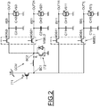
- the switching power supply comprises a switching cell CCM formed of two switches IT1 and IT2, respectively constituted in this example by a P-channel field effect transistor (PMOS transistor) powered by the supply voltage VE, and by an N-channel insulated gate field-effect transistor (NMOS transistor) connected to ground.
- the CCM switching cell here also comprises a single inductive element L connected between a first common terminal BC1 with the switch IT1, and a second common terminal BC2 with the switch IT2.
- the switching cell CCM also has several outputs OUT11-OUT1j and OUT21-OUT2i, which also form the outputs of the switching power supply.
- Each output OUT1j, OUT2i is associated with a capacitor C1j, C2i connected between this output and ground.
- the capacitor C1j, C2i, associated with each output OUT1j, OUT2i thus acts as a reservoir of energy to continue to feed the unselected output and maintain the voltage on said output, until it is again selected.
- the charges CH11 and CH21 may for example be the audio amplifier AA, and the regulated voltages VS11 and VS21 may be respectively the voltages -VS and + VS of the AA audio amplifier power supply.
- each output OUT1j is connected to the terminal BC1 via an elementary switch, here formed of a selection transistor MOS1j, which may be an N-channel or P-channel transistor.
- each output OUT2i is connected to the terminal BC2 via an elementary switch, here formed of a selection transistor MOS2i, which can also be an N-channel or P-channel transistor.
- the set of elementary switches MOS11-MOS1j form first selection means MSEL1
- the set of elementary switches MOS21-MOS2i forms second selection means MSEL2.
- the first and second selection means MSEL1, MSEL2 will make it possible to individually select the outputs of the switching power supply.
- the switching power supply is controlled by a servo-control loop so as to store a defined energy in the inductive element and then to restore this energy to the different outputs.
- the invention is not limited to this particular embodiment but also includes any type of switching power supply.
- the switching power supply may for example be devoid of a servocontrol loop and systematically restore the energy to an output after or during the storage of this energy in the inductive element.
- the switch IT1 is successively and alternately closed and open, so as to allow storage of energy in the inductive element, then a return of this energy.
- the duration during which the switch is open and closed during each conduction cycle depends on the duty cycle ⁇ .
- the energy stored in the inductive element corresponds to the total energy required by each of the outputs OUT1j, OUT2i of the power supply.
- the switching power supply ALM also comprises a control loop for controlling the switching cell to obtain the desired output voltage on each of the outputs.
- Each of the desired output voltages VS21 and VS11 is a regulated voltage whose value is set by the value of an external reference voltage VREF1 and VREF2, respectively. It is these reference voltages VREF1 and VREF2 which have for example, in the application of the cellular mobile phone evoked, opposite signs.
- the servo-control loop BAS comprises a first elementary amplification means AMP1, whose positive input receives the voltage VREF1, and whose negative input is connected to the first output terminal OUT11.
- the difference between the reference external voltage VREF1 and the output voltage VS11, is therefore amplified in the error amplifier AMP1, and the corresponding error voltage VERREUR1 is an image of the elementary energy required on the output OUT 11.
- the servo-control loop BAS likewise comprises a second elementary error amplifier AMP2 receiving, on the one hand, the reference voltage VREF2 and, on the other hand, the voltage VS21.
- This amplifier AMP2 delivers a VERREUR2 error voltage, which is also representative of the elementary energy required on the output OUT21.
- the servo-control loop BAS also includes SUMO summation means, the two inputs of which are respectively connected to the two outputs of the elementary error amplifiers AMP1 and AMP2.
- the output of the amplification means SUMO consequently delivers a voltage VERREUR0 which is representative of the total energy corresponding to the sum of the elementary energies respectively required by all the outputs during each conduction cycle.
- the servo-control loop BAS also comprises a control pre-stage formed here by several comparators CMP0, CAMP1 and CMP2.
- the comparator CMP0 here called the main comparator, receives on its negative input the error voltage VERREUR0, and on its positive input, a voltage VRAMPE corresponding to a ramp signal SRP generated in a conventional manner by a ramp generator GR structure known per se.
- the output of the main comparator CMP0 therefore delivers a main pulse control signal PWM0.
- the comparator CMP1 is a so-called “elementary” comparator, which is associated with the output OUT11. This comparator CMP1 receives on its negative input the voltage VERREUR1 and on its positive input voltage VRAMPE. It delivers an elementary pulse control signal PWM1.
- the comparator CMP2 is a so-called “elementary” comparator, associated with the output OUT21, which delivers, after having received on its two inputs the error voltage VERREUR2 and the voltage VRAMPE, an elementary pulse control signal PWM2.
- the signals PWM0, PWM1 and PWM2 are therefore pulse signals whose pulses are of width modulated by the level of the error voltage.
- the control means of the servo-control loop BAS further comprise a digital control stage ETNC, receiving the signals PWM0, PWM1, PWM2, as well as a clock signal CLK, which is moreover used to reset the generator of ramps at the beginning of each conduction cycle (this is done on the rising edge of the CLK clock, for example).
- a digital control stage ETNC receiving the signals PWM0, PWM1, PWM2, as well as a clock signal CLK, which is moreover used to reset the generator of ramps at the beginning of each conduction cycle (this is done on the rising edge of the CLK clock, for example).
- the control stage ETNC will develop from the signals PWM0, PWM1 and PWM2, control signals intended to control, on the one hand, the switches IT1 and IT2 of the control cell.
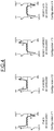
- the reference IL designates the current flowing in the inductive element L.
- the switches IT1 (PMOS transistor) and IT2 (NMOS transistor) are in conduction. They allow to inject energy into the inductive element L.
- the outputs OUT11 and OUT21 can also be selected simultaneously with the configuration No. 3, in which the transistors MOS11 and MOS21 are in conduction.
- the output OUT11 can be selected with the configuration No. 4, in which the switch IT2 and the transistor MOS11 are in conduction.
- the embodiment described thus makes it possible to keep a current in the inductive element L relatively low, even when the switching power supply is used as a voltage booster.
- the embodiment may comprise only three external components for producing two symmetrical voltages: an inductor and two capacitors.
- Transistors MOS1j and MOS2i selection means MSEL1, MSEL2 of the CCM switching cell may be N-channel or P-channel transistors. Their choice will depend on the application and the value of the regulated output voltages.
- the elementary switches of the selection means MSEL1, MSEL2 may be formed of any type of switch that can be implemented in an integrated circuit, for example bipolar transistors or IGBT transistors. It is the same for the switches IT1 and IT2.
Landscapes
- Engineering & Computer Science (AREA)
- Power Engineering (AREA)
- Dc-Dc Converters (AREA)
Claims (14)
- Schaltnetzteil (ALM) mit einer Schaltzelle (CCM), umfassend :- ein einziges induktives Element (L) mit zwei Anschlüssen (BC1, BC2) ;- mehrere individuell selektierbare Ausgänge (OUT1j, OUT2i),- zwei Schalter (IT1, IT2), jeweils geschaltet zwischen einer Versorgungsspannung (VE) und einem der Anschlüsse des induktiven Elements (L), und zwischen der Masse und einem der Anschlüsse des induktiven Elements (L)dadurch gekennzeichnet, dass die beiden Anschlüsse des induktiven Elements (L) mit jeweils wenigstens zweien der individuell selektierbaren Ausgänge verbunden sind, und dadurch, dass die Versorgung außerdem Steuereinrichtungen umfasst, die fähig sind, simultan die genannten wenigstens zwei der individuell selektierbaren Anschlüsse zu selektieren.
- Schaltnetzteil (ALM) nach Anspruch 1, bei dem die Schaltzelle (CCM) umfasst :- erste steuerbare Selektionseinrichtungen (MSEL1) mit einem mit einem ersten Anschluss (BC1) des induktiven Elements (L) verbundenen Eingangsanschluss und einem oder mehreren Ausgangsanschlüssen, jeweils angeschlossen an den Ausgang oder die Ausgänge (OUT11, OUT1j), verbunden mit dem ersten Anschluss (BC1) des induktiven Elements (L),- zweite steuerbare Selektionseinrichtungen (MSEL2) mit einem mit dem zweiten Anschluss (BC2) des induktiven Elements (L) verbundenen Eingangsanschluss und einem oder mehreren Ausgangsanschlüssen, jeweils angeschlossen an den Ausgang oder die Ausgänge (OUT21, OUT2i), verbunden mit dem zweiten Anschluss (BC2) des induktiven Elements (L), und- einen Kondensator (C1j, C2i) pro Ausgang (OUT1j, OUT2i), der einen Anschluss besitzt, der verbunden ist mit dem entsprechenden Anschluss der entsprechenden Selektionseinrichtungen.
- Schaltnetzteil (ALM) nach einem der Ansprüche 1 bis 2, ebenfalls zwei Schalter (IT1, IT2) umfassend, jeweils geschaltet zwischen einer Versorgungsspannung (VE) und einem der Anschlüsse des induktiven Elements (L), und zwischen der Masse und einem der Anschlüsse des induktiven Elements (L).
- Schaltnetzteil (ALM) nach einem der Ansprüche 1 bis 3, bei dem die Schaltzelle (CCM) zyklisch steuerbar ist durch einen Regelkreis (BAS), und bei dem der Regelkreis (BAS) Determinationsmittel umfasst, fähig bei jedem Leitzyklus eine der Summe der jeweils im Laufe dieses Zyklus von allen Ausgängen angeforderten Elementarenergien entsprechende Gesamtenergie zu bestimmen, und Steuereinrichtungen umfasst, fähig, im Laufe dieses Zyklus die Schaltzelle derart zu steuern, dass sie, eventuell in mehreren Malen, in das induktive Element die genannte Gesamtenergie einspeist, die eine Nichtnull-Elementarenergie anfordernden Ausgänge eventuell in mehreren Wiederholungen selektiert und an jeden selektierten Ausgang die entsprechende Elementarenergie abgibt.
- Schaltnetzteil nach Anspruch 4, bei dem die Steuereinrichtungen fähig sind, im Laufe jedes Leitzyklus sukzessiv und in einer für alle Zyklen identischen festgelegten Reihenfolge die Ausgänge zu selektieren, die eine Nichtnull-Elementarenergie anfordern.
- Schaltnetzteil (ALM) nach einem der Ansprüche 1 bis 5, bei dem einer der mit dem ersten Anschluss (BC1) des induktiven Elements (L) verbundenen Ausgänge (OUT11, OUT1j) und einer der mit dem zweiten Anschluss (BC2) des induktiven Elements (L) verbundenen Ausgänge (OUT21, OUT2i) Spannungen mit umgekehrten Vorzeichen und absolut gleichen Werten aufweisen.
- Endgerät eines drahtlosen Kommunikationssystems mit einem Schaltnetzteil (ALM) nach einem der Ansprüche 1 bis 6.
- Endgerät nach Anspruch 7, das ein Mobilfunktelefon bildet.
- Endgerät nach Anspruch 7 oder 8 mit einer Batterie (BAT) und einem Audioverstärker (AA), bei dem das Schaltnetzteil durch eine Batterie (BAT) des Endgeräts gespeist wird und die Regelspannung des Audioverstärkers (AA) die zwischen zwei Ausgängen vorhandene Spannungsdifferenz ist, die jeweils mit den beiden Anschlüssen des induktiven Elements des Schaltnetzteils (ALM) verbunden sind.
- Steuerverfahren eines Schaltnetzteils (ALM) mit einer Schaltzelle (CCM), umfassend ein einziges induktives Element (L) mit zwei Anschlüssen (BC1, BC2), mehreren individuell selektierbaren Ausgängen (OUT1j, OUT2i) und zwei Schalter (IT1, IT2), die jeweils zwischen einer Versorgungsspannung (VE) und einem der Anschlüsse des induktiven Elements (L) beziehungsweise zwischen der Masse und einem der Anschlüsse des induktiven Elements geschaltet sind, dadurch gekennzeichnet, dass die beiden Anschlüsse des induktiven Elements (L) mit jeweils wenigstens zweien der individuell selektierbaren Ausgänge verbunden sind, man simultan wenigstens zwei Ausgänge selektiert, die jeweils mit den beiden Anschlüssen des induktiven Elements verbunden sind.
- Verfahren nach Anspruch 10, bei dem die Schaltzelle (CCM) zyklisch steuerbar ist, und bei dem man im Laufe jedes Leitzyklus, eventuell in mehreren Malen, in das induktive Element (L) eine Gesamtenergie einspeist, die der Summe der jeweils von allen Ausgängen im Laufe dieses Zyklus angeforderten Elementarenergien entspricht, man, eventuell in mehreren Wiederholungen, die Ausgänge selektiert, die eine Nichtnull-Elementarenergie anfordern, und man an jeden selektierten Ausgang die entsprechende Elementarenergie abgibt.
- Verfahren nach Anspruch 11, bei dem man im Laufe jedes Leitzyklus sukzessiv und in einer für alle Zyklen identischen festgelegten Reihenfolge die Ausgänge selektiert, die eine Nichtnull-Elementarenergie anfordern.
- Verfahren nach einem der Ansprüche 10 bis 12, bei dem man zwei jeweils mit den Anschlüssen (BC1, BC2) des induktiven Elements (L) verbundene Ausgänge gemäß eines Befehls derart selektiert, dass man Spannungen mit umgekehrten Vorzeichen und absolut gleichen Werten erhält.
- Verfahren nach einem der Ansprüche 10 bis 13, bei dem das Schaltnetzteil (ALM) in ein Endgerät, zum Beispiel ein Mobilfunktelefon, eines drahtlosen Kommunikationssystems integriert ist, umfassend eine Batterie (BAT) und einen Audioverstärker (AA), und bei dem man das Schaltnetzteil durch eine Batterie des Endgeräts speist, und man die Spannung des Audioverstärkers mit der Spannungsdifferenz regelt, die zwischen jeweils zwei Anschlüssen des induktiven Elements des Schaltnetzteil vorhanden ist.
Applications Claiming Priority (1)
| Application Number | Priority Date | Filing Date | Title |
|---|---|---|---|
| FR0754668 | 2007-04-24 |
Publications (2)
| Publication Number | Publication Date |
|---|---|
| EP1986314A1 EP1986314A1 (de) | 2008-10-29 |
| EP1986314B1 true EP1986314B1 (de) | 2017-03-15 |
Family
ID=38658582
Family Applications (1)
| Application Number | Title | Priority Date | Filing Date |
|---|---|---|---|
| EP08103297.1A Ceased EP1986314B1 (de) | 2007-04-24 | 2008-04-01 | Steuerverfahren eines Schaltnetzteils mit einem einzigen induktiven Element und mehreren Ausgängen, sowie entsprechende Schaltnetzteilvorrichtung, insbesondere für ein Mobiltelefon |
Country Status (2)
| Country | Link |
|---|---|
| US (1) | US8614569B2 (de) |
| EP (1) | EP1986314B1 (de) |
Families Citing this family (6)
| Publication number | Priority date | Publication date | Assignee | Title |
|---|---|---|---|---|
| US8823342B2 (en) * | 2008-07-07 | 2014-09-02 | Advanced Analogic Technologies Incorporated | Multiple-output dual-polarity DC/DC converters and voltage regulators |
| WO2012032177A1 (en) * | 2010-09-10 | 2012-03-15 | St-Ericsson Sa | Symmetrical output switch-mode power supply |
| US8345030B2 (en) * | 2011-03-18 | 2013-01-01 | Qualcomm Mems Technologies, Inc. | System and method for providing positive and negative voltages from a single inductor |
| TWI514738B (zh) * | 2011-07-07 | 2015-12-21 | Sitronix Technology Corp | Voltage converter |
| TWI644300B (zh) * | 2018-01-12 | 2018-12-11 | 博發電子股份有限公司 | 單電感雙極性輸出升降壓轉換器及其控制方法 |
| US12609602B2 (en) * | 2023-12-06 | 2026-04-21 | National Cheng Kung University | Single-inductor bipolar-output converter |
Citations (1)
| Publication number | Priority date | Publication date | Assignee | Title |
|---|---|---|---|---|
| US20080231115A1 (en) * | 2007-03-16 | 2008-09-25 | Gyuha Cho | Multiple-Output DC-DC Converter |
Family Cites Families (18)
| Publication number | Priority date | Publication date | Assignee | Title |
|---|---|---|---|---|
| US5617015A (en) * | 1995-06-07 | 1997-04-01 | Linear Technology Corporation | Multiple output regulator with time sequencing |
| US6075295A (en) * | 1997-04-14 | 2000-06-13 | Micro Linear Corporation | Single inductor multiple output boost regulator |
| US6222352B1 (en) * | 1999-05-06 | 2001-04-24 | Fairchild Semiconductor Corporation | Multiple voltage output buck converter with a single inductor |
| JP2004503197A (ja) * | 2000-07-06 | 2004-01-29 | コーニンクレッカ フィリップス エレクトロニクス エヌ ヴィ | Pfm/pwmモード用多出力dc/dcコンバータ |
| KR100849355B1 (ko) * | 2001-01-17 | 2008-07-29 | 엔엑스피 비 브이 | 제어된 다중-출력 dc/dc 컨버터 |
| US6522110B1 (en) | 2001-10-23 | 2003-02-18 | Texas Instruments Incorporated | Multiple output switching regulator |
| FR2848356A1 (fr) | 2002-12-05 | 2004-06-11 | St Microelectronics Sa | Procede de commande d'une alimentation a decoupage a un seul element inductif et plusieurs sorties, et alimentation correspondante, en particulier pour un telephone mobile cellulaire |
| JP4485366B2 (ja) * | 2002-12-05 | 2010-06-23 | エヌエックスピー ビー ヴィ | 多出力dc−dcコンバータ |
| US7432614B2 (en) * | 2003-01-17 | 2008-10-07 | Hong Kong University Of Science And Technology | Single-inductor multiple-output switching converters in PCCM with freewheel switching |
| WO2005039033A1 (en) * | 2003-10-21 | 2005-04-28 | Koninklijke Philips Electronics N.V. | Voltage converter |
| CN1902810B (zh) * | 2004-01-05 | 2010-06-09 | Nxp股份有限公司 | 操作dc/dc上/下变换器的方法 |
| US7518263B2 (en) * | 2004-04-12 | 2009-04-14 | Delta Electronics, Inc. | Time delay control scheme for a power supply with multiple outputs |
| US20060176031A1 (en) * | 2005-02-04 | 2006-08-10 | Ess Technology, Inc. | Dual output switching regulator and method of operation |
| US7560914B2 (en) * | 2005-02-22 | 2009-07-14 | Artesyn Technologies, Inc. | Current-fed multiple-output power converter |
| TWI273763B (en) * | 2005-03-28 | 2007-02-11 | Richtek Technology Corp | Control apparatus and method for boost inverting converter |
| JP2006311779A (ja) * | 2005-03-31 | 2006-11-09 | Mitsumi Electric Co Ltd | 多出力型dc/dcコンバータおよびその制御方法 |
| US7276886B2 (en) * | 2005-10-03 | 2007-10-02 | Texas Instruments Incorporated | Dual buck-boost converter with single inductor |
| JP4857888B2 (ja) * | 2006-04-26 | 2012-01-18 | ミツミ電機株式会社 | 多出力型dc/dcコンバータ |
-
2008
- 2008-03-24 US US12/053,770 patent/US8614569B2/en active Active
- 2008-04-01 EP EP08103297.1A patent/EP1986314B1/de not_active Ceased
Patent Citations (1)
| Publication number | Priority date | Publication date | Assignee | Title |
|---|---|---|---|---|
| US20080231115A1 (en) * | 2007-03-16 | 2008-09-25 | Gyuha Cho | Multiple-Output DC-DC Converter |
Also Published As
| Publication number | Publication date |
|---|---|
| US8614569B2 (en) | 2013-12-24 |
| EP1986314A1 (de) | 2008-10-29 |
| US20080297127A1 (en) | 2008-12-04 |
Similar Documents
| Publication | Publication Date | Title |
|---|---|---|
| EP2104213B1 (de) | Steuerungsverfahren eines Gleichstrom/Gleichstrom-Wandlers im aussetzenden Betrieb | |
| EP2944008B1 (de) | Ladungsausgleich innerhalb einer elektrischen batterie | |
| EP2882087B1 (de) | Gleichstrom-Gleichstrom-Wandler in diskontinuierlichem Betriebsmodus | |
| EP1604447B1 (de) | In reihe geschalteter verlustarmer synchron schaltbarer spannungs-chopper | |
| EP2258036B1 (de) | Antriebsanordnung eines schaltnetzteils dc/dc mit n verschalteten speisewegen | |
| FR2848356A1 (fr) | Procede de commande d'une alimentation a decoupage a un seul element inductif et plusieurs sorties, et alimentation correspondante, en particulier pour un telephone mobile cellulaire | |
| EP1986314A1 (de) | Steuerverfahren eines Schaltnetzteils mit einem einzigen induktiven Element und mehreren Ausgängen, sowie entsprechende Schaltnetzteilvorrichtung, insbesondere für ein Mobiltelefon | |
| FR2864271A1 (fr) | Circuit de pompe a charge a rendement eleve, a faible cout | |
| EP3579233B1 (de) | Elementarzelle und ladepumpen, die eine solche elementarzelle umfassen | |
| EP0977346A1 (de) | Gleichstrom-Gleichstromwandler | |
| EP3945674A1 (de) | Spannungswandler | |
| EP4068606B1 (de) | Spannungswandler | |
| FR2884079A1 (fr) | Commande d'un transistor mos | |
| FR3029713A1 (fr) | Convertisseur continu-continu a demarrage a froid | |
| EP3654534A1 (de) | Kapazitive logische zelle | |
| EP0928060A1 (de) | Gleichspannungswandler mit verbessertem Wirkungsgrad | |
| EP3724962B1 (de) | Batterie mit geschalteten akkumulatoren | |
| EP3651363A1 (de) | Adiabatische logische zelle | |
| FR3103581A1 (fr) | Pompe de charge | |
| EP2203971B1 (de) | Verfahren zur steuerung eines schaltnetzteils und entsprechendes netzteil | |
| FR2864272A1 (fr) | Circuit de pompe a charge a rendement elevee, a faible cout | |
| EP4712329A1 (de) | Abwärtsschaltnetzteil | |
| FR3163790A1 (fr) | Convertisseur à découpage abaisseur | |
| EP1124314B1 (de) | Ladungspumpenvorrichtung | |
| FR3151162A1 (fr) | Circuit de conversion d'alimentation DC/DC |
Legal Events
| Date | Code | Title | Description |
|---|---|---|---|
| PUAI | Public reference made under article 153(3) epc to a published international application that has entered the european phase |
Free format text: ORIGINAL CODE: 0009012 |
|
| AK | Designated contracting states |
Kind code of ref document: A1 Designated state(s): AT BE BG CH CY CZ DE DK EE ES FI FR GB GR HR HU IE IS IT LI LT LU LV MC MT NL NO PL PT RO SE SI SK TR |
|
| AX | Request for extension of the european patent |
Extension state: AL BA MK RS |
|
| RIN1 | Information on inventor provided before grant (corrected) |
Inventor name: BERNARD, CHRISTOPHE Inventor name: PREMONT, CHRISTOPHE Inventor name: CHESNEAU, DAVID |
|
| 17P | Request for examination filed |
Effective date: 20090331 |
|
| 17Q | First examination report despatched |
Effective date: 20090504 |
|
| AKX | Designation fees paid |
Designated state(s): DE FR GB IT |
|
| GRAP | Despatch of communication of intention to grant a patent |
Free format text: ORIGINAL CODE: EPIDOSNIGR1 |
|
| INTG | Intention to grant announced |
Effective date: 20160927 |
|
| GRAS | Grant fee paid |
Free format text: ORIGINAL CODE: EPIDOSNIGR3 |
|
| GRAA | (expected) grant |
Free format text: ORIGINAL CODE: 0009210 |
|
| AK | Designated contracting states |
Kind code of ref document: B1 Designated state(s): DE FR GB IT |
|
| REG | Reference to a national code |
Ref country code: GB Ref legal event code: FG4D Free format text: NOT ENGLISH |
|
| REG | Reference to a national code |
Ref country code: FR Ref legal event code: PLFP Year of fee payment: 10 |
|
| REG | Reference to a national code |
Ref country code: DE Ref legal event code: R096 Ref document number: 602008049175 Country of ref document: DE |
|
| PGFP | Annual fee paid to national office [announced via postgrant information from national office to epo] |
Ref country code: FR Payment date: 20170322 Year of fee payment: 10 |
|
| PGFP | Annual fee paid to national office [announced via postgrant information from national office to epo] |
Ref country code: GB Payment date: 20170324 Year of fee payment: 10 |
|
| PGFP | Annual fee paid to national office [announced via postgrant information from national office to epo] |
Ref country code: DE Payment date: 20170321 Year of fee payment: 10 |
|
| PG25 | Lapsed in a contracting state [announced via postgrant information from national office to epo] |
Ref country code: IT Free format text: LAPSE BECAUSE OF FAILURE TO SUBMIT A TRANSLATION OF THE DESCRIPTION OR TO PAY THE FEE WITHIN THE PRESCRIBED TIME-LIMIT Effective date: 20170315 |
|
| REG | Reference to a national code |
Ref country code: DE Ref legal event code: R097 Ref document number: 602008049175 Country of ref document: DE |
|
| PLBE | No opposition filed within time limit |
Free format text: ORIGINAL CODE: 0009261 |
|
| STAA | Information on the status of an ep patent application or granted ep patent |
Free format text: STATUS: NO OPPOSITION FILED WITHIN TIME LIMIT |
|
| 26N | No opposition filed |
Effective date: 20171218 |
|
| REG | Reference to a national code |
Ref country code: DE Ref legal event code: R119 Ref document number: 602008049175 Country of ref document: DE |
|
| GBPC | Gb: european patent ceased through non-payment of renewal fee |
Effective date: 20180401 |
|
| PG25 | Lapsed in a contracting state [announced via postgrant information from national office to epo] |
Ref country code: DE Free format text: LAPSE BECAUSE OF NON-PAYMENT OF DUE FEES Effective date: 20181101 |
|
| PG25 | Lapsed in a contracting state [announced via postgrant information from national office to epo] |
Ref country code: GB Free format text: LAPSE BECAUSE OF NON-PAYMENT OF DUE FEES Effective date: 20180401 |
|
| PG25 | Lapsed in a contracting state [announced via postgrant information from national office to epo] |
Ref country code: FR Free format text: LAPSE BECAUSE OF NON-PAYMENT OF DUE FEES Effective date: 20180430 |