EP0977353A2 - Un amplificateur de transimpédance à gamme dynamique large - Google Patents
Un amplificateur de transimpédance à gamme dynamique large Download PDFInfo
- Publication number
- EP0977353A2 EP0977353A2 EP99305985A EP99305985A EP0977353A2 EP 0977353 A2 EP0977353 A2 EP 0977353A2 EP 99305985 A EP99305985 A EP 99305985A EP 99305985 A EP99305985 A EP 99305985A EP 0977353 A2 EP0977353 A2 EP 0977353A2
- Authority
- EP
- European Patent Office
- Prior art keywords
- transimpedance amplifier
- current
- input
- gain
- transistor
- Prior art date
- Legal status (The legal status is an assumption and is not a legal conclusion. Google has not performed a legal analysis and makes no representation as to the accuracy of the status listed.)
- Withdrawn
Links
- 230000003287 optical effect Effects 0.000 claims abstract description 22
- 238000000034 method Methods 0.000 claims abstract description 5
- 230000008878 coupling Effects 0.000 claims description 3
- 238000010168 coupling process Methods 0.000 claims description 3
- 238000005859 coupling reaction Methods 0.000 claims description 3
- 238000010586 diagram Methods 0.000 description 7
- 230000035945 sensitivity Effects 0.000 description 7
- 238000005516 engineering process Methods 0.000 description 6
- 230000001276 controlling effect Effects 0.000 description 4
- 229910001218 Gallium arsenide Inorganic materials 0.000 description 3
- 230000000694 effects Effects 0.000 description 3
- 230000003321 amplification Effects 0.000 description 2
- 238000013459 approach Methods 0.000 description 2
- 238000003199 nucleic acid amplification method Methods 0.000 description 2
- 239000013307 optical fiber Substances 0.000 description 2
- 230000004913 activation Effects 0.000 description 1
- 230000001419 dependent effect Effects 0.000 description 1
- 239000000835 fiber Substances 0.000 description 1
- 230000005669 field effect Effects 0.000 description 1
- 230000001105 regulatory effect Effects 0.000 description 1
Images


Classifications
-
- H—ELECTRICITY
- H03—ELECTRONIC CIRCUITRY
- H03F—AMPLIFIERS
- H03F3/00—Amplifiers with only discharge tubes or only semiconductor devices as amplifying elements
- H03F3/04—Amplifiers with only discharge tubes or only semiconductor devices as amplifying elements with semiconductor devices only
- H03F3/08—Amplifiers with only discharge tubes or only semiconductor devices as amplifying elements with semiconductor devices only controlled by light
- H03F3/087—Amplifiers with only discharge tubes or only semiconductor devices as amplifying elements with semiconductor devices only controlled by light with IC amplifier blocks
-
- H—ELECTRICITY
- H03—ELECTRONIC CIRCUITRY
- H03F—AMPLIFIERS
- H03F3/00—Amplifiers with only discharge tubes or only semiconductor devices as amplifying elements
- H03F3/45—Differential amplifiers
- H03F3/45071—Differential amplifiers with semiconductor devices only
- H03F3/45479—Differential amplifiers with semiconductor devices only characterised by the way of common mode signal rejection
Definitions
- the present invention relates to a wide dynamic range transimpedance amplifier which finds application in optical receivers.
- the invention particularly relates to a bipolar IC transimpedance amplifier.
- optical fibre networks The ever increasing demands for high capacity communications systems has seen the wide spread employment of optical fibre networks across the world.
- a fundamental component for such systems is a means of converting optical pulses comprising a digital bit stream into electrical signals. This component of such a system is commonly known as an optical receiver.
- AGC automatic gain control
- optical input power OP IN is converted into an electrical current I IN by a PIN diode photodetector 16.
- This current I IN is applied as an input to the IC optical receiver 10.
- the input current I IN is amplified by a transimpedance amplifier (Tz Amp) 18 which converts the input current I IN into an amplified voltage output signal V OUT .
- Tz Amp transimpedance amplifier
- the output voltage V OUT of the Tz Amp 18 which is in the form of a broadband data signal and may be considered as an ac, multi-frequency signal, is rectified or peak detected by a rectifier/peak detector 20 to provide a dc signal level V REC for comparison with a pre-determined dc reference voltage V REF .
- the difference between the rectified/peak detected output voltage V REC and the reference voltage V REF is considered as an error signal which is amplified and integrated by a Miller Integrator 22 to provide a control signal V CONTROL .
- a Miller Integrator is a well known form of integrator incorporating an active device such as a transistor amplifier.
- the Miller Integrator 22 is required to have a high gain, in order to ensure that the error signal approaches zero (ie in order to ensure that the difference between the rectified/peak detected output voltage V REC and the reference voltage V REF becomes zero) by means of controlling the gain of the Tz Amp by varying the impedance of a feedback resistor 24.
- the Tz Amp 18 must operate at high gain to provide high sensitivity of the optical receiver.
- the rectified/peak detected output voltage V REC becomes just greater than the dc reference voltage V REF , then the on-set of AGC occurs and continues whilst the input channel I IN increases.
- the feedback resistor 24 is at a minimum the Tz Amp is operating at very low gain and approaches an overload condition.
- the most effective method of controlling the gain of the Tz Amp 18 is to vary the value Rf of the feedback resistor 24, as shown by Fig 1.
- FETs Field Effect Transistors
- CMOS technology can offer the lowest cost but offers the poorest performance in terms of sensitivity.
- BiCMOS technology where a high performance is achieved through use of bipolar transistors for low noise while the gain control is achieved by the FET connected in parallel with the feedback resistor.
- the use of bipolar technology can achieve sensitivities comparable to GaAs MESFET technology, but poor gain control techniques may result in either lowering of the sensitivity of the receiver or providing an inadequate dynamic range.
- the invention seeks to provide a bipolar IC transimpedance amplifier including gain control.
- the invention also seeks to provide a bipolar IC transimpedance amplifier which obviates some of the problems encountered with other IC transimpedance amplifiers.
- the present invention provides a transimpedance amplifier for an optical receiver comprising an input for receiving an input current signal from a photodetector and a gain stage for amplifying the input current signal. It also comprises a resistor network coupling the output and input of the gain stage, the resistor network comprising at least first and second resistive elements in a parallel arrangement and being arranged such that one of said resistive elements can be isolated from the output of the gain stage wherein the one of said resistive elements can be isolated from the output of the gain stage by means of a transistor switching network.
- fig 1 is an oversimplification used to illustrate the general principles of operation.
- a more detailed design of a practical realisation of an optical receiver with AGC in accordance with the invention is shown in fig 2.
- the integrated circuit optical receiver 30 includes a Tz Amp 32 to amplify an input current I IN received from a photodetector 34. As in the typical receiver illustrated in fig 1, the receiver 30 includes a rectifier/peak detector 36 and integrator 38 in a control loop for providing AGC. However, the receiver 30 also includes a dummy Tz Amp 40 and a 50 ⁇ line driver 42 which provides a differential output V DIFF .
- the Tz Amp 32 and Dummy Tz Amp 40 are of the same type differing only in that the Dummy Tz Amp 40 is not connected to any input. Its purpose is to provide the correct DC voltage to bias the 50 ⁇ line driver 42.
- the 50 ⁇ line driver 42 may be a long tail pair configuration with 50 ⁇ collector resistors to interface to the outside world.
- the long tail pair configuration converts the single ended signal from the Tz Amp 32 into a differential signal at the output. This output differential signal is rectified/peak detected and compared to a reference DC voltage to determine the correct output signal level required for AGC.
- the output of the rectifier/peak detector 36 is applied to the integrator 38 to provide the required control voltages to both the Tz Amp 32 and Dummy Tz Amp 40, thus maintaining a DC match at the input of the 50 ⁇ line driver.
- An additional requirement of the integrator 38 is to provide a long time constant to prevent pattern dependent jitter of the digital data.
- a first embodiment of a bipolar IC transimpedance amplifier 50 comprises an input 52 for receiving an input current I IN signal from an optical receiver photodetector (fig 2) such as a PIN diode and a gain stage comprising first and second transistors Q1, Q2 for amplifying said input current signal I IN to provide an output voltage signal V OUT .
- the gain stage includes a feedback loop coupling its output and input comprising a parallel network of feedback resistors Rfh and Rfl.
- Rfh has a value of resistance considerably larger than Rfl, in the order of 100:1.
- the feedback resistive network establishes the gain of the gain stage.
- the network includes a transistor switching stage which enables the low value resistive element Rfl to be isolated from the gain stage input leaving only the high valve resistive element Rfh in circuit thus establishing high gain operation.
- the circuit also includes a second input 54 which receives an input voltage control signal V CONTROL to control the transistor switching network.
- the voltage control signal V CONTROL is taken from the optical receiver integrator stage (fig 2).
- the input control voltage V CONTROL determines by its action on the transistor switching network whether the low value resistive element Rfl is isolated from the gain stage input or switched in circuit.
- the control voltage (Vcontrol provided by the rectifier and integrator shown in Fig 2) would be biased to turn on fully transistors Q4 and Q5 while turning off transistors Q3 and Q6. This would result in current flow through transistor Q1 determined by the collector resistor R2. Conversely, since Q5 is turned on the current 12 would flow through resistors R1 and R3 provided just the required voltage drop to turn off transistors Q8, Q10 and in turn Q7. In addition a control current connected to the emitter of Q7 would also be turned off, isolating the feedback resistor Rfl.
- transistor Q11 While current flows through R2, transistor Q11 is biased on and connected to the feedback resistor Rfh via the emitter follower formed by transistor Q9 and resistor R6. Thus the transimpedance gain would be determined by the value of Rfh.
- the current source 13 and the resistor R4 provides the DC bias for the input of the transimpedance amplifier so that the PIN diode detector may be reversed biased. Under these conditions the current flowing in Q1 would be set to provide the lowest noise for maximum sensitivity and the majority of the current of 11 would flow through transistor Q2 to provide a virtual ac earth.
- the transistor Q12 and resistor R8 form an emitter follower output drive for the next stage.
- resistors R1, R2 and R3 are important to carefully choose the values of resistors R1, R2 and R3 such that R2>R1 and R1+R3 ⁇ R2.
- the dc control voltage 'Vcontrol' When the input current has reached a signal level requiring gain control, the dc control voltage 'Vcontrol', would begin to increase the current in Q1 by allowing current to flow in R1 and R2 while lowering the voltage drop across R1 and R3 by allowing a proportion of current 12 to flow through Q6. This would in turn begin the turn on the transistors Q8 and Q7 provided that the control current, 'Icontrol' also begins to allow current flow through transistor Q7. Since transistors Q10 and Q11 are effectively an analogue OR function, feedback is always applied to the base of Q1 via Rfh, thus the emitter of Q7 would approximately remain at a constant DC bias point.
- Vcontrol would be such that transistors Q3 and Q6 would be fully turned on while transistors Q4 and Q5 would be turned off. This would result in current flow through transistor Q1 determined by the collector resistor R1. Conversely, since Q6 is turned on the current 12 would flow through resistor R2 only, which allows transistors Q8, Q10 and in turn Q7 to be fully on since Icontrol would also be fully on. Under these conditions, re of transistor Q7 would be small compared to Rfl and Rfl would be small compared to Rfh, thus the transimpedance gain would be determined by the value of Rfl. It is important to note that for correct gain control to be achieved, the ratio of change in current from transistors Q3 to Q4 must be represented by the correct transistor ratio of Q3 and Q4.
- Icontrol is achieved by the use of a long tail pair driven by a control signal Vcontrol2 which would be derived by Vcontrol (in Fig 2) differing by a common mode voltage of only two diode drops (ie 2vbe).
- Vcontrol was steering the current through transistors Q3, Q4 and Q5, Q6, the derived Vcontrol2 would be steering the current 14 from transistor Q14 into transistor Q13, thus increasing the current through the control transistor Q7.
- Fig 5 uses the action of change of current through transistor Q2 during gain control. When high gain is required the transistor Q2 delivers a maximum collector current which in turn provides a voltage drop across R9.
- the current at the collector of transistor Q2 reduces, thus reducing the voltage drop across resistor R9.
- the regulated voltage supply 'Vregulated' in Fig 5 is required to prevent the activation of the gain control by the supply voltage variation.
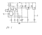
- the transimpedance amplifier with gain control illustrated in Fig 3 may be re-configured to operate with reduced voltage supply as shown by Fig 6.
Landscapes
- Engineering & Computer Science (AREA)
- Power Engineering (AREA)
- Amplifiers (AREA)
Applications Claiming Priority (2)
| Application Number | Priority Date | Filing Date | Title |
|---|---|---|---|
| GB9816529 | 1998-07-29 | ||
| GBGB9816529.3A GB9816529D0 (en) | 1998-07-29 | 1998-07-29 | A wide dynamic range transimpedance amplifier |
Publications (2)
| Publication Number | Publication Date |
|---|---|
| EP0977353A2 true EP0977353A2 (fr) | 2000-02-02 |
| EP0977353A3 EP0977353A3 (fr) | 2002-03-20 |
Family
ID=10836379
Family Applications (1)
| Application Number | Title | Priority Date | Filing Date |
|---|---|---|---|
| EP99305985A Withdrawn EP0977353A3 (fr) | 1998-07-29 | 1999-07-28 | Un amplificateur de transimpédance à gamme dynamique large |
Country Status (4)
| Country | Link |
|---|---|
| US (1) | US6297701B1 (fr) |
| EP (1) | EP0977353A3 (fr) |
| CA (1) | CA2278971A1 (fr) |
| GB (1) | GB9816529D0 (fr) |
Cited By (1)
| Publication number | Priority date | Publication date | Assignee | Title |
|---|---|---|---|---|
| CN112564652A (zh) * | 2019-09-25 | 2021-03-26 | 亚德诺半导体国际无限责任公司 | 具有可调整输入范围的跨阻抗放大器 |
Families Citing this family (22)
| Publication number | Priority date | Publication date | Assignee | Title |
|---|---|---|---|---|
| US6826372B1 (en) * | 2000-08-30 | 2004-11-30 | Sycamore Networks, Inc. | Methods and apparatus for dynamic threshold setting for an optically amplified receiver |
| US6404281B1 (en) * | 2000-11-14 | 2002-06-11 | Sirenza Microdevices, Inc. | Wide dynamic range transimpedance amplifier |
| US6529078B1 (en) * | 2001-08-22 | 2003-03-04 | Analog Devices, Inc. | Low-distortion transimpedance amplifier structures and methods |
| EP1322036A1 (fr) * | 2001-12-20 | 2003-06-25 | Koninklijke Philips Electronics N.V. | Dispositif comportant un amplificateur symétrique |
| US6803825B2 (en) | 2002-04-09 | 2004-10-12 | Microsemi Corporation | Pseudo-differential transimpedance amplifier |
| US6784750B2 (en) * | 2002-04-09 | 2004-08-31 | Microsemi Corporation | Transimpedance amplifier with selective DC compensation |
| US6771132B1 (en) * | 2002-11-26 | 2004-08-03 | Finisar Corporation | Wide dynamic range transimpedance amplifier with a controlled low frequency cutoff at high optical power |
| US6844784B1 (en) | 2002-11-26 | 2005-01-18 | Finisar Corporation | Wide dynamic range transimpedance amplifier |
| US6876260B2 (en) * | 2003-09-09 | 2005-04-05 | Gennum Corporation | Elevated front-end transimpedance amplifier |
| US7418213B2 (en) * | 2004-08-12 | 2008-08-26 | Finisar Corporation | Transimpedance amplifier with integrated filtering and reduced parasitic capacitance |
| WO2006020682A1 (fr) * | 2004-08-12 | 2006-02-23 | Triaccess Technologies, Inc. | Detecteur de niveau pour recepteurs optiques |
| US20060087378A1 (en) * | 2004-10-26 | 2006-04-27 | Hiroshi Hayakawa | Preamplifier circuit having a variable feedback resistance |
| JP2006303668A (ja) * | 2005-04-18 | 2006-11-02 | Matsushita Electric Ind Co Ltd | 出力インピーダンス可変回路 |
| US7525391B2 (en) * | 2007-05-17 | 2009-04-28 | Finisar Corporation | Linear transimpedance amplifier with multiplexed gain stage |
| US7605660B1 (en) | 2007-11-12 | 2009-10-20 | Rf Micro Devices, Inc. | Linear multi-stage transimpedance amplifier |
| US9166630B1 (en) * | 2014-07-22 | 2015-10-20 | Raytheon Company | Adaptive radio communications systems and methods |
| US9543906B2 (en) * | 2014-09-26 | 2017-01-10 | Sumitomo Electric Industries, Ltd. | Optical receiver to enhance dynamic range thereof |
| US9712117B2 (en) * | 2014-12-30 | 2017-07-18 | Skyworks Solutions, Inc. | Cascode switch for power amplifier |
| US10211861B2 (en) | 2015-03-17 | 2019-02-19 | Skyworks Solutions, Inc. | Multi-mode integrated front end module |
| US10804859B2 (en) | 2018-12-10 | 2020-10-13 | Analog Devices, Inc. | Transimpedance amplifiers with feedforward current |
| US11177775B2 (en) | 2019-12-12 | 2021-11-16 | Applied Materials Israel Ltd. | Detection circuit and method for amplifying a photosensor output current |
| US20240283419A1 (en) * | 2023-02-17 | 2024-08-22 | Semtech Corporation | Transimpedance gain control |
Family Cites Families (13)
| Publication number | Priority date | Publication date | Assignee | Title |
|---|---|---|---|---|
| DE3123919C2 (de) * | 1981-06-16 | 1983-11-17 | Siemens AG, 1000 Berlin und 8000 München | Optische Empfangsschaltung |
| US4540952A (en) * | 1981-09-08 | 1985-09-10 | At&T Bell Laboratories | Nonintegrating receiver |
| GB2209444B (en) * | 1987-07-21 | 1992-03-18 | Plessey Co Plc | Improvements in or relating to amplifiers |
| DE3938097A1 (de) * | 1989-11-16 | 1991-05-23 | Standard Elektrik Lorenz Ag | Optischer empfaenger |
| US5012202A (en) * | 1990-03-15 | 1991-04-30 | Triquint Semiconductor, Inc. | Low impedance automatic gain control circuit |
| US5202553A (en) * | 1992-03-24 | 1993-04-13 | Raynet Corporation | Enhanced performance optical receiver having means for switching between high and low amplifier configurations |
| US5451904A (en) * | 1993-03-26 | 1995-09-19 | Mitsumi Electric Co., Ltd. | Amplifying circuit in which variable impedance circuit is used in negative feedback circuit |
| US5442321A (en) * | 1993-07-08 | 1995-08-15 | Anadigics, Inc. | Automatic transimpedance control amplifier |
| US5412346A (en) * | 1993-12-13 | 1995-05-02 | At&T Corp. | Variable gain voltage signal amplifier |
| GB2288499A (en) * | 1994-03-08 | 1995-10-18 | Stewart Hughes Ltd | Gain control and capacitance correction for photodiode signal amplifier |
| US5532471A (en) * | 1994-12-21 | 1996-07-02 | At&T Corp. | Optical transimpedance amplifier with high dynamic range |
| JPH10290127A (ja) * | 1997-04-17 | 1998-10-27 | Rohm Co Ltd | 電流/電圧変換ic及び光電気変換ic |
| US6081603A (en) * | 1997-09-08 | 2000-06-27 | Information Storage Devices, Inc. | Method and apparatus for automatic gain control using a linear limiter circuit with voltage controlled resistors as a variable element |
-
1998
- 1998-07-29 GB GBGB9816529.3A patent/GB9816529D0/en not_active Ceased
-
1999
- 1999-07-28 EP EP99305985A patent/EP0977353A3/fr not_active Withdrawn
- 1999-07-28 CA CA002278971A patent/CA2278971A1/fr not_active Abandoned
- 1999-07-28 US US09/362,608 patent/US6297701B1/en not_active Expired - Lifetime
Cited By (2)
| Publication number | Priority date | Publication date | Assignee | Title |
|---|---|---|---|---|
| CN112564652A (zh) * | 2019-09-25 | 2021-03-26 | 亚德诺半导体国际无限责任公司 | 具有可调整输入范围的跨阻抗放大器 |
| CN112564652B (zh) * | 2019-09-25 | 2025-01-10 | 亚德诺半导体国际无限责任公司 | 具有可调整输入范围的跨阻抗放大器 |
Also Published As
| Publication number | Publication date |
|---|---|
| GB9816529D0 (en) | 1998-09-30 |
| US6297701B1 (en) | 2001-10-02 |
| CA2278971A1 (fr) | 2000-01-29 |
| EP0977353A3 (fr) | 2002-03-20 |
Similar Documents
| Publication | Publication Date | Title |
|---|---|---|
| US6297701B1 (en) | Wide dynamic range transimpedance amplifier | |
| US5844445A (en) | Feedback type pre-amplifier | |
| US6084478A (en) | Transimpedance amplifier with automatic gain control | |
| EP0632941B1 (fr) | Recepteur optique | |
| US6064507A (en) | High speed differential optoelectronic receiver | |
| US5363064A (en) | Preamplifier for optical communication having a gain control circuit | |
| US5734300A (en) | Optical receiver preamplifier dynamic range enhancing circuit and method | |
| JPH06177664A (ja) | ディジタル光受信回路とトランスインピーダンスアンプ回路とプリアンプ回路 | |
| US6114913A (en) | Transimpedance amplifiers with improved gain-bandwidth product | |
| US5382920A (en) | Circuit arrangement for an optical receiver | |
| US6879217B2 (en) | Triode region MOSFET current source to bias a transimpedance amplifier | |
| EP0977358B1 (fr) | Circuit intégrateur utilisant un amplificateur | |
| USH965H (en) | Differential amplifier with digitally controlled gain | |
| US4115741A (en) | Fast attack automatic gain control circuit | |
| US7221229B2 (en) | Receiver circuit having an optical reception device | |
| CA2480608A1 (fr) | Amplificateur a transimpedance dote d'un etage d'entree a elevation | |
| US4344044A (en) | Gain-controlled amplifier utilizing variable emitter degeneration and collector load impedance | |
| US5767662A (en) | Amplifier having single-ended input and differential output and method for amplifying a signal | |
| US6750712B1 (en) | Method and apparatus for voltage clamping in feedback amplifiers using resistors | |
| US3970948A (en) | Controller gain signal amplifier | |
| US4612662A (en) | Control circuit | |
| US5119041A (en) | High gain differential current amplifier having a low output voltage | |
| US4329713A (en) | Television automatic gain control system | |
| GB2074410A (en) | Variable emitter degeneration gain-controlled amplifier | |
| US4689506A (en) | Control circuit for use with electronic attenuators and method for providing a control signal proportional to absolute temperature |
Legal Events
| Date | Code | Title | Description |
|---|---|---|---|
| PUAI | Public reference made under article 153(3) epc to a published international application that has entered the european phase |
Free format text: ORIGINAL CODE: 0009012 |
|
| AK | Designated contracting states |
Kind code of ref document: A2 Designated state(s): AT BE CH CY DE DK ES FI FR GB GR IE IT LI LU MC NL PT SE Kind code of ref document: A2 Designated state(s): DE FR GB IT |
|
| AX | Request for extension of the european patent |
Free format text: AL;LT;LV;MK;RO;SI |
|
| RAP1 | Party data changed (applicant data changed or rights of an application transferred) |
Owner name: NORTEL NETWORKS LIMITED |
|
| PUAL | Search report despatched |
Free format text: ORIGINAL CODE: 0009013 |
|
| AK | Designated contracting states |
Kind code of ref document: A3 Designated state(s): AT BE CH CY DE DK ES FI FR GB GR IE IT LI LU MC NL PT SE |
|
| AX | Request for extension of the european patent |
Free format text: AL;LT;LV;MK;RO;SI |
|
| RIC1 | Information provided on ipc code assigned before grant |
Free format text: 7H 03F 3/08 A, 7H 03F 3/45 B, 7H 03G 3/30 B |
|
| 17P | Request for examination filed |
Effective date: 20020920 |
|
| AKX | Designation fees paid |
Free format text: DE FR GB IT |
|
| 17Q | First examination report despatched |
Effective date: 20030520 |
|
| RAP1 | Party data changed (applicant data changed or rights of an application transferred) |
Owner name: NORTEL NETWORKS LIMITED |
|
| GRAP | Despatch of communication of intention to grant a patent |
Free format text: ORIGINAL CODE: EPIDOSNIGR1 |
|
| STAA | Information on the status of an ep patent application or granted ep patent |
Free format text: STATUS: THE APPLICATION HAS BEEN WITHDRAWN |
|
| 18W | Application withdrawn |
Effective date: 20040715 |