EP0977362B1 - Frequenzverdoppler mit 50% Tastverhältnis am Ausgang - Google Patents
Frequenzverdoppler mit 50% Tastverhältnis am Ausgang Download PDFInfo
- Publication number
- EP0977362B1 EP0977362B1 EP98830467A EP98830467A EP0977362B1 EP 0977362 B1 EP0977362 B1 EP 0977362B1 EP 98830467 A EP98830467 A EP 98830467A EP 98830467 A EP98830467 A EP 98830467A EP 0977362 B1 EP0977362 B1 EP 0977362B1
- Authority
- EP
- European Patent Office
- Prior art keywords
- capacitor
- input
- input signal
- clk
- voltage
- Prior art date
- Legal status (The legal status is an assumption and is not a legal conclusion. Google has not performed a legal analysis and makes no representation as to the accuracy of the status listed.)
- Expired - Lifetime
Links
Images

Classifications
-
- H—ELECTRICITY
- H03—ELECTRONIC CIRCUITRY
- H03K—PULSE TECHNIQUE
- H03K5/00—Manipulating of pulses not covered by one of the other main groups of this subclass
- H03K5/00006—Changing the frequency
-
- H—ELECTRICITY
- H03—ELECTRONIC CIRCUITRY
- H03K—PULSE TECHNIQUE
- H03K5/00—Manipulating of pulses not covered by one of the other main groups of this subclass
- H03K5/156—Arrangements in which a continuous pulse train is transformed into a train having a desired pattern
- H03K5/1565—Arrangements in which a continuous pulse train is transformed into a train having a desired pattern the output pulses having a constant duty cycle
Definitions
- the present invention relates to digital circuits and more in particular to a circuit for doubling the frequency of a digital signal of a 50% duty cycle, typically of a clock signal.
- the output signal with double frequency retains a precise 50% duty cycle.
- the output signal is often used to derive an internal frequency of four times the frequency of the input signal and any deviation from a precise 50% duty cycle could induce an error in the higher frequency signals that may be derived therefrom.
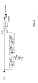
- Fig. 1 is shown a classical circuit used for doubling the frequency of an input signal with a 50% duty cycle.
- the circuit employs an EXNOR or an EXOR gate, to a first input of which is coupled the digital input signal CLK while at the second input of which is fed a replica of the input signal CLK delayed by a quarter of period by the use of a delay line including a cascade of three identical inverters and a capacitor connected between the coupling node of the output of the first inverter to the input of the second inverter and ground.
- the delay introduced by the line must be exactly a quarter of the period time of the input signal CLK.
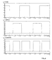
- Fig. 2 are shown the wave form of the signals, the output signal of the EXNOR gate employed being high when its two inputs are at different states.
- the circuit of this invention relies on sensing, by the use of a comparator, when the voltage on a capacitor charged with a constant current during a phase of the input signal of 50% duty cycle reaches a half of its full charge swing.
- the comparator output switches at exactly a quarter of the period of the input signal.
- the latter may be made up of two capacitors of identical value connected in series, whereby the comparator may sense the voltage present on one of the two capacitors in series.
- Constant current generator means and switch means controlled by the input signal and by its inverse signal or by functionally equivalent control signals, operatively provide for a linear charging of the capacitor or capacitors in series, during a first half period of the input signal and a complete discharge of the capacitor or of the capacitors in series during the following half period of the input signal, or anyhow after the switching of the half-swing sensing comparator.
- the output gate that can be used may either be an EXNOR or an EXOR gate, as in a prior art circuit.
- the capacitor charging and discharging circuit and the relative comparator may be "duplicated" according to a common dual architecture of digital circuitry.
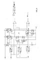
- the first input of the EXNOR output gate is coupled to the input signal CLK while the second input is coupled to the output of the comparator COMP 1.
- the comparator COMP 1 senses the voltage present on the capacitor C1a which has the same capacitance value of the capacitor C1b, connected in series thereto.
- the capacitors in series C1a and C1b are charged with a constant current generated by the current generator I1 during one phase of the input signal CLK and are discharged during the successive phase of the input signal CLK.
- the charging and discharging processes are controlled by the switches S1 and S1a and S1b.
- a dual duplication of the circuit is constituted by the current generator I2, the capacitors in series C2a and C2b, that may have of the same capacitance value of the pair C1a and C1b, the switches S2, S2a and S2b and the comparator COMP2.
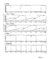
- the dual signals of opposite phase output by the comparators COMP1 and COMP2 will be exactly delayed by a quarter of the period time of the input signal CLK in respect of the corresponding transitions of the input signal CLK.
- the signals output by the two comparators COMP1 and COMP2 may be conveniently used for controlling the switches.
- FIG. 4 A circuit implementation of the basic circuit of Fig. 3 is shown in Fig. 4, illustrating also the drives that implement the switches that control the charging and discharging processes of the two pairs of capacitors in series.
- a single capacitor may be employed and half of the voltage on it be sensed by the use of a resistive voltage divider functionally connected in parallel to the capacitor, according to a common arrangement.
- circuit of the invention may employ a single comparator instead of two comparators of the dual implementation of the circuit shown in Figures 3 and 4, by employing additional switches for switching the inputs of the single comparator on one or on the other sensing line, according to common switcheable configuration techniques of integrated circuits.
Landscapes
- Physics & Mathematics (AREA)
- Nonlinear Science (AREA)
- Manipulation Of Pulses (AREA)
Claims (3)
- Frequenzverdoppler, der ein Ausgangssignal mit einem Tastgrad von 50 % besitzt und ein Doppeleingangs-EXOR- oder EXNOR-Gatter verwendet, wovon ein Eingang mit einem digitalen Eingangssignal einer ersten Frequenz (CLK) gekoppelt ist und ein zweiter Eingang mit einer Kopie des Eingangssignals, die um eine Viertelperiode des Eingangssignals (CLK) verzögert ist, gekoppelt ist, gekennzeichnet durch
wenigstens einen ersten Kondensator (C1a, C1b), einen Konstantstromgenerator (I1) zum Laden des Kondensators (C1a, C1b) während einer der beiden Halbperioden des Eingangssignals (CLK) und erste (S1) und zweite (S1a, S1b) Schaltmittel, die mit entgegengesetzter Phase durch das Eingangssignal (CLK) und durch ein invertiertes Signal hiervon (CLKN) gesteuert werden, um den Kondensator (C1a, C1b) während jeder Periode des Eingangssignals zu laden und zu entladen;
Spannungsteilermittel, die die am Kondensator (C1a, C1b) vorhandene Spannung halbieren;
wenigstens einen Komparator (COMP1), der die halbierte Spannung erfaßt und mit seinem Ausgang mit dem zweiten Eingang des Doppeleingangs-Gatters gekoppelt ist. - Frequenzverdoppler nach Anspruch 1, bei dem die Spannungsteilermittel durch Verwendung zweier in Reihe geschalteter Kondensatoren mit gleicher Kapazität (C1a, C1b), die durch den Konstantstromgenerator (I1) und die Schaltmittel (s1, S1a, S1b) geladen und entladen werden, verwirklicht sind, wobei der Komparator (COMP1) die Spannung an einem (1a) der beiden in Reihe geschalteten Kondensatoren erfaßt.
- Frequenzverdoppler nach Anspruch 1, ferner gekennzeichnet durch
einen zweiten Kondensator (C2a, C2b), einen zweiten Konstantstromgenerator (I2) zum Laden des zweiten Kondensators (2a, 2b) während einer der beiden Halbperioden des Eingangssignals (CLK) und dritte und vierte Schaltmittel (S2, S2a, S2b), die in entgegengesetzter Phase durch das digitale Eingangssignal (CLK) und durch ein invertiertes Signal hiervon (CLKN) gesteuert werden, um den zweiten Kondensator (C2a, C2b) während jeder Periode des Eingangssignals zu laden und zu entladen;
zweite Spannungsteilermittel, die die über den zweiten Kondensator (C2a, C2b) liegende Spannung halbieren;
wenigstens einen zweiten Komparator (COMP2), der die halbierte Spannung erfaßt und ein logisches Steuersignal für die Schaltmittel ausgibt.
Priority Applications (3)
| Application Number | Priority Date | Filing Date | Title |
|---|---|---|---|
| EP98830467A EP0977362B1 (de) | 1998-07-30 | 1998-07-30 | Frequenzverdoppler mit 50% Tastverhältnis am Ausgang |
| DE69808611T DE69808611T2 (de) | 1998-07-30 | 1998-07-30 | Frequenzverdoppler mit 50% Tastverhältnis am Ausgang |
| US09/358,047 US6348821B1 (en) | 1998-07-30 | 1999-07-21 | Frequency doubler with 50% duty cycle output |
Applications Claiming Priority (1)
| Application Number | Priority Date | Filing Date | Title |
|---|---|---|---|
| EP98830467A EP0977362B1 (de) | 1998-07-30 | 1998-07-30 | Frequenzverdoppler mit 50% Tastverhältnis am Ausgang |
Publications (2)
| Publication Number | Publication Date |
|---|---|
| EP0977362A1 EP0977362A1 (de) | 2000-02-02 |
| EP0977362B1 true EP0977362B1 (de) | 2002-10-09 |
Family
ID=8236736
Family Applications (1)
| Application Number | Title | Priority Date | Filing Date |
|---|---|---|---|
| EP98830467A Expired - Lifetime EP0977362B1 (de) | 1998-07-30 | 1998-07-30 | Frequenzverdoppler mit 50% Tastverhältnis am Ausgang |
Country Status (3)
| Country | Link |
|---|---|
| US (1) | US6348821B1 (de) |
| EP (1) | EP0977362B1 (de) |
| DE (1) | DE69808611T2 (de) |
Families Citing this family (13)
| Publication number | Priority date | Publication date | Assignee | Title |
|---|---|---|---|---|
| DE10036722C1 (de) * | 2000-07-27 | 2002-02-28 | Infineon Technologies Ag | Frequenzverdopplungsschaltung |
| JP2005236600A (ja) * | 2004-02-19 | 2005-09-02 | Matsushita Electric Ind Co Ltd | 高周波2逓倍回路 |
| US6967508B2 (en) * | 2004-03-04 | 2005-11-22 | Texas Instruments Incorporated | Compact frequency doubler/multiplier circuitry |
| FR2879374B1 (fr) * | 2004-12-15 | 2007-03-02 | Commissariat Energie Atomique | Dispositif doubleur de frequence |
| KR100934222B1 (ko) * | 2007-08-29 | 2009-12-29 | 한국전자통신연구원 | 고해상도의 정전용량-시간 변환 회로 |
| KR20130102398A (ko) * | 2012-03-07 | 2013-09-17 | 삼성전자주식회사 | 반도체 메모리 장치의 병렬 비트 테스트 회로 |
| CN103368528B (zh) * | 2013-07-26 | 2016-12-28 | 上海华虹宏力半导体制造有限公司 | 振荡器 |
| US9531358B2 (en) * | 2014-10-27 | 2016-12-27 | Mediatek Inc. | Signal generating system and signal generating method |
| US10998892B1 (en) | 2020-08-13 | 2021-05-04 | Realtek Semiconductor Corp. | Frequency doubler with duty cycle control and method thereof |
| US11309875B2 (en) | 2020-08-13 | 2022-04-19 | Realtek Semiconductor Corp. | Frequency doubler using recirculating delay circuit and method thereof |
| WO2021092601A2 (en) * | 2020-09-25 | 2021-05-14 | Futurewei Technologies, Inc. | Techniques for calibrating 50% duty cycle differential frequency doubler |
| CN113036942B (zh) * | 2021-03-12 | 2022-10-25 | 哈尔滨工业大学 | 一种超级电容的无线充电系统 |
| US12609679B2 (en) * | 2023-08-09 | 2026-04-21 | Nxp B.V. | Quadrature phase shifted clock generation with duty cycle correction |
Family Cites Families (6)
| Publication number | Priority date | Publication date | Assignee | Title |
|---|---|---|---|---|
| DD103535A1 (de) * | 1973-03-19 | 1974-01-20 | ||
| JPS6116416A (ja) | 1984-07-03 | 1986-01-24 | 日立電線株式会社 | 油入電力ケ−ブル |
| JPS61116416A (ja) * | 1984-11-09 | 1986-06-03 | Nec Corp | 二逓倍クロツク抽出回路 |
| JPH01320814A (ja) * | 1988-05-23 | 1989-12-26 | Advanced Micro Devicds Inc | 一連の入力パルスの周波数を逓倍するための回路 |
| JP2563156B2 (ja) * | 1992-09-22 | 1996-12-11 | インダストリアル テクノロジー リサーチ インスティチュート | クロック再生回路 |
| US5630228A (en) * | 1995-04-24 | 1997-05-13 | Motorola, Inc. | Double balanced mixer circuit with active filter load for a portable comunication receiver |
-
1998
- 1998-07-30 DE DE69808611T patent/DE69808611T2/de not_active Expired - Lifetime
- 1998-07-30 EP EP98830467A patent/EP0977362B1/de not_active Expired - Lifetime
-
1999
- 1999-07-21 US US09/358,047 patent/US6348821B1/en not_active Expired - Lifetime
Also Published As
| Publication number | Publication date |
|---|---|
| DE69808611T2 (de) | 2003-02-06 |
| DE69808611D1 (de) | 2002-11-14 |
| US6348821B1 (en) | 2002-02-19 |
| EP0977362A1 (de) | 2000-02-02 |
Similar Documents
| Publication | Publication Date | Title |
|---|---|---|
| EP0977362B1 (de) | Frequenzverdoppler mit 50% Tastverhältnis am Ausgang | |
| EP0053014B1 (de) | Taktgeberschaltung | |
| US5159205A (en) | Timing generator circuit including adjustable tapped delay line within phase lock loop to control timing of signals in the tapped delay line | |
| US9178497B2 (en) | Precision oscillator with temperature compensation | |
| KR0162148B1 (ko) | 프로그램 가능한 듀티 사이클 컨버터 및 변환 방법 | |
| JP2877205B2 (ja) | 2相ノンオーバラップ信号生成回路 | |
| WO2023077694A1 (zh) | 一种rc振荡电路 | |
| EP0465249B1 (de) | Spannungsvergleichsschaltung mit Abtast-Halte-Schaltungsanordnung und deren Benutzung in einem Analog-Digital-Wandler | |
| US5539348A (en) | Precise delay line circuit with predetermined reset time limit | |
| EP0328339B1 (de) | Frequenzteilerschaltung | |
| US6967508B2 (en) | Compact frequency doubler/multiplier circuitry | |
| CA1094172A (en) | Digitally synthesized back-up frequency | |
| EP0773627A1 (de) | Flipflop-Schaltung | |
| CN206506516U (zh) | 电路装置 | |
| WO2004045064A1 (en) | Differential time sampling circuit | |
| KR0132483B1 (ko) | 디지탈 자기기록재생시스템의 데이타 추출회로 | |
| JPS5636225A (en) | Phase comparing circuit | |
| KR100246330B1 (ko) | 발진기 | |
| US20070001737A1 (en) | System and method of generating a clock cycle having an asymmetric duty cycle | |
| JPH05242979A (ja) | ガス放電ランプを点灯させるための自励パルス発生回路 | |
| SU1693714A1 (ru) | Фазовый детектор | |
| JP2564300B2 (ja) | ダイナミツク型フリツプフロツプ | |
| JPS62109288A (ja) | 論理回路 | |
| JPH1198416A (ja) | 電荷結合素子の駆動回路 | |
| JP3673037B2 (ja) | 波形整形回路 |
Legal Events
| Date | Code | Title | Description |
|---|---|---|---|
| PUAI | Public reference made under article 153(3) epc to a published international application that has entered the european phase |
Free format text: ORIGINAL CODE: 0009012 |
|
| AK | Designated contracting states |
Kind code of ref document: A1 Designated state(s): DE FR GB IT |
|
| AX | Request for extension of the european patent |
Free format text: AL;LT;LV;MK;RO;SI |
|
| 17P | Request for examination filed |
Effective date: 20000323 |
|
| AKX | Designation fees paid |
Free format text: DE FR GB IT |
|
| GRAG | Despatch of communication of intention to grant |
Free format text: ORIGINAL CODE: EPIDOS AGRA |
|
| 17Q | First examination report despatched |
Effective date: 20011026 |
|
| GRAG | Despatch of communication of intention to grant |
Free format text: ORIGINAL CODE: EPIDOS AGRA |
|
| GRAH | Despatch of communication of intention to grant a patent |
Free format text: ORIGINAL CODE: EPIDOS IGRA |
|
| RTI1 | Title (correction) |
Free format text: FREQUENCY DOUBLER WITH 50% DUTY CYCLE OUTPUT |
|
| GRAH | Despatch of communication of intention to grant a patent |
Free format text: ORIGINAL CODE: EPIDOS IGRA |
|
| GRAA | (expected) grant |
Free format text: ORIGINAL CODE: 0009210 |
|
| AK | Designated contracting states |
Kind code of ref document: B1 Designated state(s): DE FR GB IT |
|
| REG | Reference to a national code |
Ref country code: GB Ref legal event code: FG4D |
|
| REF | Corresponds to: |
Ref document number: 69808611 Country of ref document: DE Date of ref document: 20021114 |
|
| ET | Fr: translation filed | ||
| PLBE | No opposition filed within time limit |
Free format text: ORIGINAL CODE: 0009261 |
|
| STAA | Information on the status of an ep patent application or granted ep patent |
Free format text: STATUS: NO OPPOSITION FILED WITHIN TIME LIMIT |
|
| 26N | No opposition filed |
Effective date: 20030710 |
|
| PGFP | Annual fee paid to national office [announced via postgrant information from national office to epo] |
Ref country code: IT Payment date: 20060731 Year of fee payment: 9 |
|
| PGFP | Annual fee paid to national office [announced via postgrant information from national office to epo] |
Ref country code: FR Payment date: 20070730 Year of fee payment: 10 |
|
| REG | Reference to a national code |
Ref country code: FR Ref legal event code: ST Effective date: 20090331 |
|
| PG25 | Lapsed in a contracting state [announced via postgrant information from national office to epo] |
Ref country code: FR Free format text: LAPSE BECAUSE OF NON-PAYMENT OF DUE FEES Effective date: 20080731 |
|
| PG25 | Lapsed in a contracting state [announced via postgrant information from national office to epo] |
Ref country code: IT Free format text: LAPSE BECAUSE OF NON-PAYMENT OF DUE FEES Effective date: 20070730 |
|
| PGFP | Annual fee paid to national office [announced via postgrant information from national office to epo] |
Ref country code: GB Payment date: 20100628 Year of fee payment: 13 Ref country code: DE Payment date: 20100706 Year of fee payment: 13 |
|
| GBPC | Gb: european patent ceased through non-payment of renewal fee |
Effective date: 20110730 |
|
| PG25 | Lapsed in a contracting state [announced via postgrant information from national office to epo] |
Ref country code: DE Free format text: LAPSE BECAUSE OF NON-PAYMENT OF DUE FEES Effective date: 20120201 |
|
| REG | Reference to a national code |
Ref country code: DE Ref legal event code: R119 Ref document number: 69808611 Country of ref document: DE Effective date: 20120201 |
|
| PG25 | Lapsed in a contracting state [announced via postgrant information from national office to epo] |
Ref country code: GB Free format text: LAPSE BECAUSE OF NON-PAYMENT OF DUE FEES Effective date: 20110730 |