EP0979002A2 - Méthode et appareil de détection de l'atténuation d'image dans un signal vidéo - Google Patents
Méthode et appareil de détection de l'atténuation d'image dans un signal vidéo Download PDFInfo
- Publication number
- EP0979002A2 EP0979002A2 EP99115249A EP99115249A EP0979002A2 EP 0979002 A2 EP0979002 A2 EP 0979002A2 EP 99115249 A EP99115249 A EP 99115249A EP 99115249 A EP99115249 A EP 99115249A EP 0979002 A2 EP0979002 A2 EP 0979002A2
- Authority
- EP
- European Patent Office
- Prior art keywords
- fade
- video signal
- value
- absolute value
- difference
- Prior art date
- Legal status (The legal status is an assumption and is not a legal conclusion. Google has not performed a legal analysis and makes no representation as to the accuracy of the status listed.)
- Granted
Links
Images



Classifications
-
- H—ELECTRICITY
- H04—ELECTRIC COMMUNICATION TECHNIQUE
- H04N—PICTORIAL COMMUNICATION, e.g. TELEVISION
- H04N19/00—Methods or arrangements for coding, decoding, compressing or decompressing digital video signals
- H04N19/85—Methods or arrangements for coding, decoding, compressing or decompressing digital video signals using pre-processing or post-processing specially adapted for video compression
- H04N19/87—Methods or arrangements for coding, decoding, compressing or decompressing digital video signals using pre-processing or post-processing specially adapted for video compression involving scene cut or scene change detection in combination with video compression
-
- H—ELECTRICITY
- H04—ELECTRIC COMMUNICATION TECHNIQUE
- H04N—PICTORIAL COMMUNICATION, e.g. TELEVISION
- H04N5/00—Details of television systems
- H04N5/14—Picture signal circuitry for video frequency region
- H04N5/147—Scene change detection
Definitions
- the present invention relates to a fade detection by which a fade-in or fade-out state of an image is detected based on a video signal.
- a fade detecting apparatus which uses the video signal itself for the detection of fade-in or fade-out state (hereinafter, referred to simply as a fade state) such that the luminance of a whole image gradually increases or decreases with the lapse of time.
- the total luminance value of the video signal corresponding to one frame is compared with the total luminance value of the video signal corresponding to a frame which is one frame before (or after) the above frame.
- a difference value between them is kept constant for a predetermined period, a determination is made that the video signal is in the fade state, and a fade detection signal is produced.
- the invention has been made to solve the problem and it is an object of the invention to provide fade detecting method and apparatus of a video signal, in which a fade state of an image can be detected from the video signal at a high speed.
- a fade detecting method of a video signal for detecting a fade-in or fade-out state of an image from an original video signal constituted by a series of pixel data corresponding to pixels of a picture comprising: a first fade discriminating step of obtaining, as a first difference absolute value, an absolute value of a difference between the total luminance value of the original video signal of one frame and the total luminance value of neighboring video signal of one frame which are neighboring just before or just after the original video signal, and discriminating whether the first difference absolute value is larger than a first predetermined value or not; a second fade discriminating step of obtaining, as a second difference absolute value, an absolute value of a difference between each pixel data in the original video signal of one frame and each pixel data in the neighboring video signal with respect to pixels existing at a spatially same position, and discriminating whether the number of pixels in which the second difference absolute value is smaller than a second predetermined value is larger than a predetermined number or not; and a fade detecting
- a fade detecting apparatus of a video signal for detecting a fade-in or fade-out state of an image from an original video signal constructed by a series of pixel data corresponding to pixels of a picture, comprising: delay means for delaying the original video signal by one frame period and obtaining a delayed original video signal; first subtracting means for obtaining, as a first difference absolute value, an absolute value of a difference between the total luminance value of the original video signal of one frame and the total luminance value of the delayed original video signal; first comparing means for comparing whether the first difference absolute value is larger than a first predetermined value or not; second subtracting means for obtaining, as a second difference absolute value, an absolute value of a difference between each pixel data in the original video signal of one frame and each pixel data in the delayed original video signal with respect to pixels existing at a spatially same position; second comparing means for detecting that the second difference absolute value is smaller than a second predetermined value; counting means for counting the number of pixels in which it is detected
- Fig. 1 is a diagram schematically showing the construction of a fade detecting apparatus embodied based on a method of detecting fade of a video signal according to the invention.
- a video data D n constructed by a series of pixel data samples each corresponding to each pixel on a display picture is sequentially written into a frame memory 20 every pixel data sample.
- the signals are read out from the frame memory 20 in accordance with the writing order. That is, the frame memory 20 delays the video data D n by one frame period and generates the delayed signal.
- a delayed video data D n-1 delayed by one frame period by the frame memory 20 and read out therefrom is supplied to a fade discriminating circuit 100.
- the video data D n and delayed video data D n-1 which is one frame before the video data D n are supplied to the fade discriminating circuit 100.
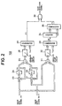
- Fig. 2 is a diagram showing an example of an internal construction of the fade discriminating circuit 100.
- a first accumulation adding circuit comprising an adder 21 and a D flip-flop 22 accumulates and adds the pixel data samples in the delayed video data D n-1 , thereby obtaining the sum of luminance values.
- the storage contents of the D flip-flop 22 are reset each time the pixel data samples of one frame are accumulated and added.
- the sum of the luminance values which is finally obtained by the first accumulation adding circuit is, therefore, equal to the total luminance value of one frame of the image in the delayed video data D n-1 and it is generated as a total luminance value Y n-1 from the D flip-flop 22.
- a second accumulation adding circuit comprising an adder 23 and a D flip-flop 24 accumulates and adds the pixel data samples in the video data D n , thereby obtaining the sum of luminance values.
- the storage contents of the D flip-flop 24 are reset each time the pixel data samples of one frame are accumulated and added.
- the sum of the luminance values which is finally obtained by the second accumulation adding circuit is, therefore, equal to the total luminance value of one frame of the image in the video data D n and it is generated as a total luminance value Y n from the D flip-flop 24.
- a subtractor 25 obtains a difference value between the total luminance values Y n and Y n-1 and supplies it to an absolute value circuit 26.
- the absolute value circuit 26 supplies the absolute value of the difference value to a comparator 27.
- the comparator 27 compares whether the absolute value of the difference between the total luminance values Y n and Y n-1 is larger than a predetermined value T to or not. When it is larger than T to , the comparator 27 generates a first fade discrimination signal F1 at the logic level "1". When it is smaller, the comparator 27 generates the first fade discrimination signal F1 at the logic level "0".
- the comparator supplies the signal F1 to an AND gate circuit 30.
- the construction comprising the first and second accumulation adding circuits, subtractor 25, absolute value circuit 26, and comparator 27, the absolute value of the difference between the total luminance value Y n of the video data D n in the nth frame and the total luminance value Y n-1 of the delayed video data D n-1 in the (n-1)th frame is obtained, and the first fade discrimination signal F1 at the logic level "1" is generated only when the absolute value is larger than the predetermined value T to .
- a subtractor 31 sequentially obtains a difference value between each pixel data sample in the video data D n and each pixel data sample in the delayed video data D n-1 which is one-frame preceding to the video data D n , and supplies it to an absolute value circuit 32.
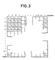
- pixel data samples corresponding to pixels G 11 to G xy on the display picture are labelled to DS 11 to DS xy and the pixel data samples of the nth frame and the pixel data samples of the (n-1)th frame are expressed as follows.
- the subtractor 31 obtains the difference between each pixel data sample of the nth frame and each pixel data sample of the (n-1)th frame in the pixels corresponding to the pixels existing at the same position on the display picture. That is, the subtractor 31 obtains
- the absolute value circuit 32 sequentially supplies the absolute values of the difference values to a comparator 33.
- the comparator 33 compares whether the above-mentioned absolute value of the difference between the pixel data sample of the nth frame and the pixel data sample of the (n-1)th frame is smaller than a predetermined value T pi or not.
- the absolute value circuit 32 generates a clock pulse CP and supplies it to a counter 34 so long as it is smaller than T pi .
- the counter 34 counts the number of clock pulses CP supplied from the comparator 33 and supplies a count value to a comparator 35. In this instance, the counter 34 resets the count value to 0 each time the comparing process of one frame by the comparator 33 is finished.
- the comparator 35 compares whether the count value is larger than a predetermined value T ra or not. When it is larger than T ra , the comparator 35 generates a second fade discrimination signal F2 at the logic level "1". When it is smaller than T ra , the comparator 35 generates the signal F2 at the logic level "0". The comparator 35 supplies the signal F2 to the AND gate circuit 30.
- the absolute value of the difference between each pixel data sample in the nth frame and each pixel data sample in the (n-1)th frame is sequentially obtained with respect to the pixels existing at the spatially same position.
- the number of pixel data samples in each of which the absolute value is smaller than the predetermined value T pi is counted. Only when its count value is larger than a predetermined value T ra , the second fade discrimination signal F2 at the logic level "1" is generated.
- the AND gate circuit 30 When both the first and second fade discrimination signals F1 and F2 are at the logic level “1", the AND gate circuit 30 produces a fade detection signal of the logic level "1" indicating that the image based on the video data D n is in the fade state. When at least one of the first and second fade discrimination signals F1 and F2 is at the logic level "0”, the AND gate circuit 30 produces a fade detection signal of the logic level "0" indicating that the image based on the video data D n is not in the fade state.
- the fade detecting apparatus shown in Figs. 1 and 2 realizes the fade detection by paying attention to a point that the image is in the fade state in the case where the following two conditions (1) and (2) are satisfied between the video data D n of one frame constructing the image and the delayed video data D n-1 which is one-frame precedent thereto.
- the fade detection as mentioned above is performed by using the video data D n and the delayed video data D n-1 which is one-frame precedent thereto.
- the fade detection can be also similarly performed by using a video data D n+1 which is one-frame subsequent thereto.
- the image based on the original video signal is in the fade state, in the case where the absolute value of the difference between the total luminance value of the original video signal of one frame and the total luminance value of the neighboring video signal of one frame which are neighboring just before or after the original video signal is relatively large, and the number of pixels in which the absolute value of the difference between each pixel data in the original video signal of one frame and each pixel data in the neighboring video signal is relatively small with respect to the pixels existing at the spatially same position is large.
- the fade discriminating circuit 100 is constituted by the hardware as shown in Fig. 2, the corresponding operation can be realized by software.
- the fade discriminating circuit 100 is formed for example by a microcomputer shown in Fig. 4 which comprises a CPU (Central Processing Unit) 101, an RAM (Random Access Memory) 101, and an ROM (Read Only Memory) 102 mutually connected by an address bus 105 and a data bus 106.
- the reference numeral 104 represents an I/O interface which serves for inputting the video data and delayed video data to the microcomputer, for example, in such a way that the video data and the delayed video data are assigned to the upper bits and the lower bits of the data bus 106.
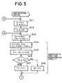
- the CPU 101 performs the fade detection by a procedure as shown in Figs. 5 and 6 in accordance with the software previously stored in the ROM 103.
- the CPU 101 first allows "0" to be stored into the RAM 102 as an initial value of each of the total luminance value Y n in all image data of the nth frame and the total luminance value Y n-1 in all image data of the (n-1)th frame luminance value Y n-1 in all image data of the (n-1) th frame (step S41). Subsequently, the CPU 101 allows "0" to be stored into the RAM 102 as an initial value of a count value CNT (step S42).
- the CPU 101 subsequently fetches one pixel data sample in the video data D n , allows it to be stored into the RAM 102 as a pixel data sample DS n , fetches one pixel data sample in the delayed video data D n-1 , and allows it to be stored into the RAM 102 as a pixel data sample DS n-1 (step S43).
- the CPU 101 now overwrites the total luminance values onto the RAM 102 in a manner such that the value obtained by adding the pixel data sample DS n to the total luminance value Y n is set to the new total luminance value Y n and the value obtained by adding the pixel data sample DS n-1 to the total luminance value Y n-1 is set to the new total luminance value Y n-1 (step S44).
- the CPU 101 calculates the absolute value between the total luminance values Y n and Y n-1 and allows it to be stored into the RAM 102 as a luminance difference value YS (step S45).
- the CPU 101 discriminates whether the luminance difference value YS is larger than the predetermined value T to or not (step S46).
- step S46 When it is determined in step S46 that the luminance difference value YS is larger than the predetermined value T to , the CPU 101 overwrites the logic level predetermined value T to , the CPU 101 overwrites the logic level "1" into the area in the RAM 102 where the first fade discrimination signal F1 should be written (step S47).
- step S46 When it is determined in step S46 that the luminance difference value YS is not larger than the predetermined value T to , the CPU 101 overwrites the logic level "0" into the area in the RAM 102 where the first fade discrimination signal F1 should be written (step S48).
- the CPU 101 calculates the absolute value of the difference between the pixel data samples DS n and DS n-1 fetched in step S43 and allows it to be stored as a pixel difference value GS in the RAM 102 (step S49).
- the CPU 101 discriminates whether the pixel difference value GS is smaller than the predetermined value T pi or not (step S50). When it is determined in step S50 that the pixel difference value GS is smaller than the predetermined value T pi , the CPU 101 overwrites the logic level "1" into the area in the RAM 102 where the second fade discrimination signal F2 should be written (step S53).
- step S52 When it is determined in step S52 that the pixel difference value GS is not smaller than the predetermined value T pi , the CPU 101 overwrites the logic level "0" into the area in the RAM 102 where the second fade discrimination signal F2 should be written (step S54).
- step S53 or S54 the CPU 101 discriminates whether the processes for one frame have been finished or not (step S55).
- step S55 the CPU 101 executes a discrimination about whether the one sample period has elapsed from the end of the fetching of the pixel data samples DS n and DS n-1 or not in step S43 until the one sample period elapses (step S56).
- step S56 the CPU 101 returns to the execution in step S43 and repetitively executes a series of operations as mentioned above.
- step S57 the CPU 101 discriminates whether the first fade discrimination signal F1 is at the logic level "1" or not (step S57).
- step S57 the CPU 101 discriminates whether the second fade discrimination signal F2 is at the logic level "1" or not (step S58).
- step S58 the second fade discrimination signal F2 is at the logic level "1"
- the CPU 101 produces the fade detection signal of the logic level "1" (step S59).
- step S57 When it is determined in step S57 that the first fade discrimination signal F1 is not at the logic level "1" or when it is decided in step S58 that the second fade discrimination signal F2 is not at the logic level "1", the CPU 101 produces the fade detection signal of the logic level "0" (step S60). After completion of step S59 or S60, the CPU 101 returns to the execution in step S41 and repetitively executes the operations as mentioned above.
- the high speed image process can be performed in real-time.
Landscapes
- Engineering & Computer Science (AREA)
- Multimedia (AREA)
- Signal Processing (AREA)
- Studio Circuits (AREA)
Applications Claiming Priority (2)
| Application Number | Priority Date | Filing Date | Title |
|---|---|---|---|
| JP22337498A JP3724956B2 (ja) | 1998-08-06 | 1998-08-06 | 画像信号のフェード検出方法及びフェード検出装置 |
| JP22337498 | 1998-08-06 |
Publications (3)
| Publication Number | Publication Date |
|---|---|
| EP0979002A2 true EP0979002A2 (fr) | 2000-02-09 |
| EP0979002A3 EP0979002A3 (fr) | 2003-05-14 |
| EP0979002B1 EP0979002B1 (fr) | 2006-10-18 |
Family
ID=16797153
Family Applications (1)
| Application Number | Title | Priority Date | Filing Date |
|---|---|---|---|
| EP19990115249 Expired - Lifetime EP0979002B1 (fr) | 1998-08-06 | 1999-08-02 | Méthode et appareil de détection de l'atténuation d'image dans un signal vidéo |
Country Status (4)
| Country | Link |
|---|---|
| US (1) | US6542544B1 (fr) |
| EP (1) | EP0979002B1 (fr) |
| JP (1) | JP3724956B2 (fr) |
| DE (1) | DE69933624T2 (fr) |
Cited By (1)
| Publication number | Priority date | Publication date | Assignee | Title |
|---|---|---|---|---|
| EP1037469A3 (fr) * | 1999-03-08 | 2003-06-18 | Pioneer Corporation | Dispositif et procédé de détection de fondu enchaíné et de codage de l'information correspondante |
Families Citing this family (2)
| Publication number | Priority date | Publication date | Assignee | Title |
|---|---|---|---|---|
| US7356084B2 (en) * | 2003-10-09 | 2008-04-08 | Samsung Electronics Co., Ltd. | Method for tracking the disappearance of detected logos within digital video signals |
| JP5621734B2 (ja) | 2011-08-29 | 2014-11-12 | Nttエレクトロニクス株式会社 | フェード種別判定装置 |
Family Cites Families (8)
| Publication number | Priority date | Publication date | Assignee | Title |
|---|---|---|---|---|
| DE68909271T2 (de) * | 1988-02-23 | 1994-03-24 | Philips Nv | Verfahren und Anordnung zum Abschätzen des Bewegungsausmasses bei einem Bildelement eines Fernsehbildes. |
| JP2861249B2 (ja) * | 1989-05-11 | 1999-02-24 | 日本電気株式会社 | 画像変化検出方法および画像変化検出装置 |
| US5245436A (en) * | 1992-02-14 | 1993-09-14 | Intel Corporation | Method and apparatus for detecting fades in digital video sequences |
| US5686963A (en) * | 1995-12-26 | 1997-11-11 | C-Cube Microsystems | Method for performing rate control in a video encoder which provides a bit budget for each frame while employing virtual buffers and virtual buffer verifiers |
| US5920360A (en) * | 1996-06-07 | 1999-07-06 | Electronic Data Systems Corporation | Method and system for detecting fade transitions in a video signal |
| US6061471A (en) * | 1996-06-07 | 2000-05-09 | Electronic Data Systems Corporation | Method and system for detecting uniform images in video signal |
| US6084641A (en) * | 1997-08-06 | 2000-07-04 | General Instrument Corporation | Fade detector for digital video |
| US6259733B1 (en) * | 1998-06-16 | 2001-07-10 | General Instrument Corporation | Pre-processing of bit rate allocation in a multi-channel video encoder |
-
1998
- 1998-08-06 JP JP22337498A patent/JP3724956B2/ja not_active Expired - Fee Related
-
1999
- 1999-08-02 DE DE1999633624 patent/DE69933624T2/de not_active Expired - Fee Related
- 1999-08-02 EP EP19990115249 patent/EP0979002B1/fr not_active Expired - Lifetime
- 1999-08-02 US US09/365,027 patent/US6542544B1/en not_active Expired - Fee Related
Cited By (2)
| Publication number | Priority date | Publication date | Assignee | Title |
|---|---|---|---|---|
| EP1037469A3 (fr) * | 1999-03-08 | 2003-06-18 | Pioneer Corporation | Dispositif et procédé de détection de fondu enchaíné et de codage de l'information correspondante |
| US6625214B1 (en) | 1999-03-08 | 2003-09-23 | Pioneer Corporation | Apparatus and method for fade detecting and information encoding |
Also Published As
| Publication number | Publication date |
|---|---|
| EP0979002A3 (fr) | 2003-05-14 |
| JP2000059683A (ja) | 2000-02-25 |
| DE69933624T2 (de) | 2007-08-23 |
| DE69933624D1 (de) | 2006-11-30 |
| EP0979002B1 (fr) | 2006-10-18 |
| US6542544B1 (en) | 2003-04-01 |
| JP3724956B2 (ja) | 2005-12-07 |
Similar Documents
| Publication | Publication Date | Title |
|---|---|---|
| US5963272A (en) | Method and apparatus for generating a reference image from an image sequence | |
| CN113673454B (zh) | 遗留物检测方法、相关设备和存储介质 | |
| US20180376102A1 (en) | Profile for frame rate conversion | |
| JP4213035B2 (ja) | オクルージョン領域を検出するオクルージョン検出器および方法 | |
| EP0979002B1 (fr) | Méthode et appareil de détection de l'atténuation d'image dans un signal vidéo | |
| US8331676B2 (en) | Image processing apparatus and method, and program | |
| US6188798B1 (en) | Apparatus and method for detecting motion vector | |
| CN106780646B (zh) | 一种适用多场景的无参数背景建模方法 | |
| US20200065979A1 (en) | Imaging system and method with motion detection | |
| KR980007495A (ko) | 잡음 감소와 히스토그램 등화를 이용한 화질 개선회로 및 그 방법 | |
| JP2009542080A (ja) | 大域的動き推定方法 | |
| KR100532990B1 (ko) | 카메라의 움직임 검출 방법 | |
| CN116760968A (zh) | 一种视频播放效果检测方法、装置及计算机可读存储介质 | |
| JP3833076B2 (ja) | 映像信号処理装置、映像信号の処理方法及び映像信号の処理方法のプログラム | |
| JP2005229166A (ja) | 映像信号のノイズ量測定装置および測定方法 | |
| JP3505851B2 (ja) | 画像表示装置 | |
| KR100351160B1 (ko) | 영상 움직임 보상 장치 및 방법 | |
| JP3276823B2 (ja) | 映像信号処理回路 | |
| US20090116751A1 (en) | Image Discrimination Apparatus | |
| JP2006237695A (ja) | プルダウン検出装置及びプルダウン検出方法 | |
| CN115018882B (zh) | 一种跟踪方法、装置、设备及介质 | |
| US20240020850A1 (en) | Method and optical motion sensor capable of identifying false motion | |
| CN120223954A (zh) | 一种视频画面静帧判定方法 | |
| JPH0750815A (ja) | 動き補正画像処理方式 | |
| JPH07220076A (ja) | 画像処理装置 |
Legal Events
| Date | Code | Title | Description |
|---|---|---|---|
| PUAI | Public reference made under article 153(3) epc to a published international application that has entered the european phase |
Free format text: ORIGINAL CODE: 0009012 |
|
| AK | Designated contracting states |
Kind code of ref document: A2 Designated state(s): AT BE CH CY DE DK ES FI FR GB GR IE IT LI LU MC NL PT SE |
|
| AX | Request for extension of the european patent |
Free format text: AL;LT;LV;MK;RO;SI |
|
| PUAL | Search report despatched |
Free format text: ORIGINAL CODE: 0009013 |
|
| AK | Designated contracting states |
Designated state(s): AT BE CH CY DE DK ES FI FR GB GR IE IT LI LU MC NL PT SE |
|
| AX | Request for extension of the european patent |
Extension state: AL LT LV MK RO SI |
|
| RIC1 | Information provided on ipc code assigned before grant |
Ipc: 7H 04N 7/26 B Ipc: 7H 04N 5/14 A |
|
| 17P | Request for examination filed |
Effective date: 20030703 |
|
| AKX | Designation fees paid |
Designated state(s): DE FR GB |
|
| 17Q | First examination report despatched |
Effective date: 20040524 |
|
| GRAP | Despatch of communication of intention to grant a patent |
Free format text: ORIGINAL CODE: EPIDOSNIGR1 |
|
| GRAS | Grant fee paid |
Free format text: ORIGINAL CODE: EPIDOSNIGR3 |
|
| GRAA | (expected) grant |
Free format text: ORIGINAL CODE: 0009210 |
|
| AK | Designated contracting states |
Kind code of ref document: B1 Designated state(s): DE FR GB |
|
| REG | Reference to a national code |
Ref country code: GB Ref legal event code: FG4D |
|
| REF | Corresponds to: |
Ref document number: 69933624 Country of ref document: DE Date of ref document: 20061130 Kind code of ref document: P |
|
| ET | Fr: translation filed | ||
| PLBE | No opposition filed within time limit |
Free format text: ORIGINAL CODE: 0009261 |
|
| STAA | Information on the status of an ep patent application or granted ep patent |
Free format text: STATUS: NO OPPOSITION FILED WITHIN TIME LIMIT |
|
| 26N | No opposition filed |
Effective date: 20070719 |
|
| GBPC | Gb: european patent ceased through non-payment of renewal fee |
Effective date: 20070802 |
|
| REG | Reference to a national code |
Ref country code: FR Ref legal event code: ST Effective date: 20080430 |
|
| PG25 | Lapsed in a contracting state [announced via postgrant information from national office to epo] |
Ref country code: DE Free format text: LAPSE BECAUSE OF NON-PAYMENT OF DUE FEES Effective date: 20080301 |
|
| PG25 | Lapsed in a contracting state [announced via postgrant information from national office to epo] |
Ref country code: FR Free format text: LAPSE BECAUSE OF NON-PAYMENT OF DUE FEES Effective date: 20070831 |
|
| PG25 | Lapsed in a contracting state [announced via postgrant information from national office to epo] |
Ref country code: GB Free format text: LAPSE BECAUSE OF NON-PAYMENT OF DUE FEES Effective date: 20070802 |