EP0981152A2 - Hochgeschwindigkeits-"Flip-Chip"-Abgabevorrichtung - Google Patents
Hochgeschwindigkeits-"Flip-Chip"-Abgabevorrichtung Download PDFInfo
- Publication number
- EP0981152A2 EP0981152A2 EP99306116A EP99306116A EP0981152A2 EP 0981152 A2 EP0981152 A2 EP 0981152A2 EP 99306116 A EP99306116 A EP 99306116A EP 99306116 A EP99306116 A EP 99306116A EP 0981152 A2 EP0981152 A2 EP 0981152A2
- Authority
- EP
- European Patent Office
- Prior art keywords
- chip
- carrier tape
- chip carrier
- chips
- tape
- Prior art date
- Legal status (The legal status is an assumption and is not a legal conclusion. Google has not performed a legal analysis and makes no representation as to the accuracy of the status listed.)
- Granted
Links
Images



Classifications
-
- H—ELECTRICITY
- H10—SEMICONDUCTOR DEVICES; ELECTRIC SOLID-STATE DEVICES NOT OTHERWISE PROVIDED FOR
- H10P—GENERIC PROCESSES OR APPARATUS FOR THE MANUFACTURE OR TREATMENT OF DEVICES COVERED BY CLASS H10
- H10P72/00—Handling or holding of wafers, substrates or devices during manufacture or treatment thereof
- H10P72/04—Apparatus for manufacture or treatment
- H10P72/0442—Apparatus for placing on an insulating substrate, e.g. tape
-
- H—ELECTRICITY
- H10—SEMICONDUCTOR DEVICES; ELECTRIC SOLID-STATE DEVICES NOT OTHERWISE PROVIDED FOR
- H10P—GENERIC PROCESSES OR APPARATUS FOR THE MANUFACTURE OR TREATMENT OF DEVICES COVERED BY CLASS H10
- H10P72/00—Handling or holding of wafers, substrates or devices during manufacture or treatment thereof
- H10P72/04—Apparatus for manufacture or treatment
- H10P72/0446—Apparatus for mounting on conductive members, e.g. leadframes or conductors on insulating substrates
-
- H—ELECTRICITY
- H10—SEMICONDUCTOR DEVICES; ELECTRIC SOLID-STATE DEVICES NOT OTHERWISE PROVIDED FOR
- H10P—GENERIC PROCESSES OR APPARATUS FOR THE MANUFACTURE OR TREATMENT OF DEVICES COVERED BY CLASS H10
- H10P72/00—Handling or holding of wafers, substrates or devices during manufacture or treatment thereof
- H10P72/30—Handling or holding of wafers, substrates or devices during manufacture or treatment thereof for conveying, e.g. between different workstations
- H10P72/32—Handling or holding of wafers, substrates or devices during manufacture or treatment thereof for conveying, e.g. between different workstations between different workstations
- H10P72/3212—Handling or holding of wafers, substrates or devices during manufacture or treatment thereof for conveying, e.g. between different workstations between different workstations the substrates to be conveyed not being semiconductor wafers or large planar substrates, e.g. chips or lead frames
-
- H—ELECTRICITY
- H10—SEMICONDUCTOR DEVICES; ELECTRIC SOLID-STATE DEVICES NOT OTHERWISE PROVIDED FOR
- H10P—GENERIC PROCESSES OR APPARATUS FOR THE MANUFACTURE OR TREATMENT OF DEVICES COVERED BY CLASS H10
- H10P72/00—Handling or holding of wafers, substrates or devices during manufacture or treatment thereof
- H10P72/30—Handling or holding of wafers, substrates or devices during manufacture or treatment thereof for conveying, e.g. between different workstations
- H10P72/33—Handling or holding of wafers, substrates or devices during manufacture or treatment thereof for conveying, e.g. between different workstations into and out of processing chamber
- H10P72/3311—Horizontal transfer of a batch of workpieces
-
- H—ELECTRICITY
- H10—SEMICONDUCTOR DEVICES; ELECTRIC SOLID-STATE DEVICES NOT OTHERWISE PROVIDED FOR
- H10P—GENERIC PROCESSES OR APPARATUS FOR THE MANUFACTURE OR TREATMENT OF DEVICES COVERED BY CLASS H10
- H10P72/00—Handling or holding of wafers, substrates or devices during manufacture or treatment thereof
- H10P72/70—Handling or holding of wafers, substrates or devices during manufacture or treatment thereof for supporting or gripping
- H10P72/78—Handling or holding of wafers, substrates or devices during manufacture or treatment thereof for supporting or gripping using vacuum or suction, e.g. Bernoulli chucks
-
- H—ELECTRICITY
- H10—SEMICONDUCTOR DEVICES; ELECTRIC SOLID-STATE DEVICES NOT OTHERWISE PROVIDED FOR
- H10W—GENERIC PACKAGES, INTERCONNECTIONS, CONNECTORS OR OTHER CONSTRUCTIONAL DETAILS OF DEVICES COVERED BY CLASS H10
- H10W72/00—Interconnections or connectors in packages
- H10W72/071—Connecting or disconnecting
- H10W72/0711—Apparatus therefor
-
- H—ELECTRICITY
- H10—SEMICONDUCTOR DEVICES; ELECTRIC SOLID-STATE DEVICES NOT OTHERWISE PROVIDED FOR
- H10W—GENERIC PACKAGES, INTERCONNECTIONS, CONNECTORS OR OTHER CONSTRUCTIONAL DETAILS OF DEVICES COVERED BY CLASS H10
- H10W72/00—Interconnections or connectors in packages
- H10W72/071—Connecting or disconnecting
- H10W72/0711—Apparatus therefor
- H10W72/07173—Means for moving chips, wafers or other parts, e.g. conveyor belts
-
- Y—GENERAL TAGGING OF NEW TECHNOLOGICAL DEVELOPMENTS; GENERAL TAGGING OF CROSS-SECTIONAL TECHNOLOGIES SPANNING OVER SEVERAL SECTIONS OF THE IPC; TECHNICAL SUBJECTS COVERED BY FORMER USPC CROSS-REFERENCE ART COLLECTIONS [XRACs] AND DIGESTS
- Y10—TECHNICAL SUBJECTS COVERED BY FORMER USPC
- Y10T—TECHNICAL SUBJECTS COVERED BY FORMER US CLASSIFICATION
- Y10T29/00—Metal working
- Y10T29/53—Means to assemble or disassemble
- Y10T29/5313—Means to assemble electrical device
- Y10T29/53191—Means to apply vacuum directly to position or hold work part
Definitions
- This invention relates to techniques and related apparatus for semiconductor chip handling and more specifically to methods for transferring chips from chip carrier tapes to other processing stations.
- a variety of systems for conveying finished integrated circuit (IC) chips from the IC singulation operation to the IC packaging operation are available commercially. Many of these systems use an apertured punched plastic carrier tape with a pressure sensitive adhesive backing, hereinafter referred to as carrier tape, as more particularly described in Industry Standard, EIA/IS-747, published by the Electronic Industries Association, Arlington, Va. Chips are mounted in the apertures with a pick and place tool, and are retained in the apertures by the pressure sensitive adhesive backing, hereinafter referred to as adhesive backing.
- a widely used carrier tape system uses two parallel rails of adhesive backing which extend along the underside of the apertured plastic tape, hereinafter referred to as the plastic carrier. See, e.g. U.S. Patent No. 5,203,143, issued April 20, 1993.
- the tapes can be conveyed directly to the next assembly operation, or more typically, are reeled for temporary storage. Tapes are then unreeled and the chips are picked from the carrier tape to be placed in a package assembly machine. With conventional pick and place tools the chips, which are carried circuit side up on the carrier tape, are seized on the circuit side by the vacuum head of the pick and place machine, and inserted circuit side up in the next assembly station. For normal surface mount and wire bonded packages the circuit side up position of the chip is the orientation desired. However, for flip-chip packages, this orientation is upside down.
- the carrier tape for flip-chip assembly where the chip can be loaded on the carrier tape circuit side up in the usual manner, and can be picked from the carrier tape and placed circuit side down in a single pick operation.
- the system uses essentially the same equipment used in the conventional arrangement, and uses essentially the same carrier tape.
- the carrier tape has a new design specifically intended for this invention, and in yet other embodiments the apparatus is modified to create the new carrier tape in situ.
- the feature that is common to all embodiments, according to the invention is to pick the chip from the back side of the carrier tape. The vacuum head of the pick tool then contacts the back side of the IC chip, and dispenses the chip circuit side down without any additional handling.
- the adhesive backing of the tape is advantageously modified by providing discrete apertures at the chip sites in place of the continuous dual rail adhesive backing.
- an adhesive backed punched plastic carrier tape is shown at 11 with sprocket holes 12 for controllably reeling the tape through the dispensing apparatus.
- the sprocket holes also serve as alignment means for coordinating the movement of the tape and the pick and place tools.
- the chip sites are shown at 19 which are simply openings through the carrier tape 11.
- the IC chips are shown at 14, and rest on the adhesive backing rails 13.
- the rails 13 are coated on the chip side of the rails with a low adhesion polymer to retain the chips in place.
- the adhesive backing can be any of a variety of flexible tapes.
- a well known example is Nitto tape which is widely used in the industry.
- the plastic carrier can be any suitable thick flexible high strength material.
- SurfTape® manufactured by Tempo Electronics, Los Angeles, Calif.
- the processed wafers are singulated in a dicing machine and the individual chips are placed in a carrier tape 11 as shown in Fig. 1.
- the tape may be conveyed as a conveyer belt to a subsequent processing station but is more typically reeled and the reel is taken to the first packaging station.
- the individual chips are dispensed from the tape by a pick and place tool and placed in a die bonder or mounted on an interconnect substrate for solder bonding.
- the chips 14 are solder bumped with solder bumps 15, and ready for surface mounting on an interconnect substrate.
- the typical dispensing operation is shown in Figs. 2-4, where the unreeled tape 11 is stepped through a dispensing apparatus and the individual die 14 are picked from the carrier tape 11 by the pick and place tool 16.
- the pick and place tool is conventional and typically consists of a vacuum head 21 attached to a micromanipulator arm that picks the chips from the carrier tape and places them on the package substrate (not shown).
- the dispensing operation is enabled with the use of a die ejector pin 17, which as shown in Fig. 3, lifts the chip 14 from the carrier tape 13 to engage the vacuum head 21 of the pick and place tool 16.
- the carrier tape is stepped into position for this operation by sprockets that engage the sprocket holes 12.
- the operation of the pick and place tool, the die ejector pin, and the movement of the carrier tape are coordinated in a manner that allows chips to be dispensed at a rate of several per second.
- the timing of the operation of the die ejector pin and the vacuum head are such that the adhesive backing of the carrier tape peels from the back of the chip as shown in Fig. 3, prior to raising the vacuum head, so that twisting or rotation of the chip is minimized.
- Fig. 4 shows the dispensing operation completed, and the chip ready to be moved to the placement site.
- the modification of the dispensing operation according to the invention is shown in Figs. 5-7.
- the essential feature of this modified dispensing operation is that the carrier tape and the pick tool are oriented so that the active side of the chips are facing the vacuum head of the pick tool. Since the chips are loaded onto the carrier tape at the singulation stage with the active side up, i.e. the back of the chip contacts the adhesive backing 13, either the tape or the vacuum head must be inverted with respect to each other.
- the carrier tape is inverted and inserted "upside down" into the dispensing apparatus. This can be achieved following one of several options.
- the carrier tape can be reeled "backwards" from the singulation operation.
- the carrier tape can be re-reeled to reverse the tape.
- the carrier tape can be inverted in the dispensing equipment.
- Yet another option is to exchange the position of the pick and place vacuum head and the die ejector pin in the configuration shown in Fig. 5, and use the carrier tape in the conventional orientation. In this mode the die ejector pin pushes from the top and the vacuum head picks from the bottom. The pick and place tool is then rotated 180° to place the chip. Rotating the vacuum head is relatively simple and rapid compared with interjecting an additional pick and place operation as in the prior art approach.
- the carrier tape is stepped to the dispensing station with the carrier tape oriented upside down with respect to the ejector pin and pick tool.
- the essence of the invention is the recognition that the chip can be pushed through the bottom of the carrier tape rather than lifted from the top. This is shown in Fig. 5 where the ejector pin 17 and the chip 14 are on the same side of the adhesive backing 13, and the ejector pin engages the active side of the chip 14 rather than the back side as in Figs. 2-4. Since the ejector pin is incident on the circuit side of the chip it is preferred in this arrangement for the ejector pin to be provided with a pad 18 to reduce the risk of damage to the IC and to inhibit rotational movement of the die during release from the adhesive backing.
- Typical IC chips at this stage in the fabrication sequence have a protective coating of SINCAPS or polyimide covering the surface of the IC metallization in part to reduce the incidence of damage in handling and packaging.
- the additional precaution of padding the ejector tip may be taken.
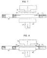
- Fig. 6 The dispensing sequence of the invention is continued in Fig. 6 wherein the chip 14 is shown being pushed through the bottom of the carrier tape 11. It has been demonstrated that the ejection of the chip through the adhesive backing 13 in the manner shown can be achieved reliably and rapidly.
- the dispensing operation is shown completed in Fig. 7, with chip 14 oriented with active side down, as required for the placement of the flip-chip on the interconnection substrate.
- the dispensing operation of the invention may be further aided by the use of an aperture plate, as shown at 19 in Fig. 8.
- the aperture plate is a simple frame that is positioned as shown during lift-off of the chip 14 from the adhesive backing 13. This expedient is especially useful when the chip is relatively small, i.e. when a relatively large gap exists between the edge of the chip and the edge of the opening in the carrier tape.
- Other means for facilitating lift-off may also be found helpful.
- the tape edges can be serrated or slit.
- the back of the chips may be roughened to decrease the adhesive force between the tape and the chip.
- Figs. 9-14 the adhesive backing on the carrier tape is a single adhesive tape, with a width greater than the chip width, and the adhesive backing is provided with individual apertures at the chip sites.
- the variation between embodiments is primarily in the shape of the aperture.
- a modified carrier tape is shown at 21, with square (or optionally rectangular) windows 22 at the chip sites as shown.
- the windows 22 are the openings in the thick plastic carrier. Portions of the adhesive backing for the carrier tape appear at 23 in each of the windows 22.
- the apertures in the adhesive backing are shown at 24.
- Sprocket holes in the carrier tape are shown at 25.
- the chips, after mounting on the tape, will occupy the space shown in phantom.
- the adhesive backing, separated from the plastic carrier, is shown in Fig. 10.
- the apertures 24, as evident from the chips shown in phantom in Fig. 9, are larger than the chip area.
- Each aperture 24 is provided with one or more tabs 27, which provide the adhesive contact surfaces for holding the chips.
- FIG. 11 Another embodiment of a carrier tape with discrete apertures in the adhesive backing is shown in Fig. 11.
- the continuous carrier tape is shown at 31, with windows 32, portions of the adhesive backing 33, apertures 34 in the adhesive backing, and sprocket holes 35.
- the chip sites are shown in phantom.
- the adhesive backing 33, separated from the plastic carrier 31, is shown in Fig. 12.
- the apertures 34 are larger than the chip area, but additional tabs 38 are provided which, in combination with tabs 37, ensure adhesive contact with each of the four edges of the chip.
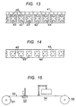
- FIG. 13 A further embodiment of a carrier tape with discrete apertures in the adhesive backing is shown in Fig. 13.
- the continuous carrier tape is shown at 41, with windows 42, portions of the adhesive backing 43, apertures 44 in the adhesive backing, and sprocket holes 45.
- the chip sites are shown in phantom.
- the adhesive backing 43, separated from the plastic carrier 41, is shown in Fig. 14.
- the apertures 44 are larger than the chip area.
- the tabs 45 ensure adhesive tab contact with each of the four edges of the chip.
- the carrier tape designs of Figs. 9-14 represent preferred embodiments of the invention.
- the apertures may be smaller than the chips, so that the adhesive contact area extends around the periphery of the chips. In this case it is desirable to have a plurality of slits at the edges of the apertures.
- Another alternative is to form apertures with length L and width W, to accommodate chips with length L 1 and width W 1 , where L>L 1 and W ⁇ W 1 , or where L ⁇ L 1 and W>W 1 .
- the apertures in the adhesive backing are custom fitted to the size of the chips being carried.
- the custom fit may be approached using different strategies.
- the adhesive backing on the carrier tapes can be pre-punched by the carrier tape supplier, and provided to the assembly operation in punched form.
- the adhesive backing on the carrier tapes is punched in situ, i.e., as part of the initial chip sorting operation.
- a suitable apparatus for achieving this is shown schematically in Fig. 15.
- the new carrier tape is provided reeled on reel 51.
- the carrier tape 52 is passed first into a punch station 53 where the adhesive backing on the carrier tape is punched to form apertures custom fitted to the chips being processed.
- the carrier tape then proceeds to a loading station 54, where the chips are loaded onto the tape carrier with a conventional pick and place tool.
- the loaded tape is then reeled on take up reel 55 to be ready for the next assembly operation.
- the means for conveying the carrier tape from one station to another generally comprises drive sprockets which engage the sprocket holes in the carrier tape and coordinate the movement of the tape with the station operations.
- the adhesive backing can alternatively be punched and then applied to the plastic carrier.
- the adhesive backing can be made wide enough to extend over the sprocket holes of the carrier tape.
- the adhesive backing is punched with sprocket holes corresponding to those of the carrier tape in the same operation used for punching the apertures. Other means of registration will occur to those skilled in the art.
- solder bumps and solder bumped chips refers to the use of solder interconnections of any form or configuration, e.g. balls, paste etc.
Landscapes
- Packages (AREA)
- Supply And Installment Of Electrical Components (AREA)
- Wire Bonding (AREA)
- Packaging Frangible Articles (AREA)
- Container, Conveyance, Adherence, Positioning, Of Wafer (AREA)
Applications Claiming Priority (2)
| Application Number | Priority Date | Filing Date | Title |
|---|---|---|---|
| US09/134,843 US6205745B1 (en) | 1998-05-27 | 1998-08-14 | High speed flip-chip dispensing |
| US134843 | 1998-08-14 |
Publications (3)
| Publication Number | Publication Date |
|---|---|
| EP0981152A2 true EP0981152A2 (de) | 2000-02-23 |
| EP0981152A3 EP0981152A3 (de) | 2004-01-02 |
| EP0981152B1 EP0981152B1 (de) | 2010-12-01 |
Family
ID=22465270
Family Applications (1)
| Application Number | Title | Priority Date | Filing Date |
|---|---|---|---|
| EP99306116A Expired - Lifetime EP0981152B1 (de) | 1998-08-14 | 1999-08-02 | Hochgeschwindigkeits-"Flip-Chip"-Abgabevorrichtung |
Country Status (6)
| Country | Link |
|---|---|
| US (1) | US6205745B1 (de) |
| EP (1) | EP0981152B1 (de) |
| JP (2) | JP3554682B2 (de) |
| KR (2) | KR100667602B1 (de) |
| DE (1) | DE69942991D1 (de) |
| TW (1) | TW417266B (de) |
Cited By (18)
| Publication number | Priority date | Publication date | Assignee | Title |
|---|---|---|---|---|
| WO2001078111A1 (de) * | 2000-04-10 | 2001-10-18 | Infineon Technologies Ag | Vorrichtung zum handling von bauelementen |
| EP1336986A3 (de) * | 2002-01-28 | 2006-08-16 | Motorola, Inc. | Verfahren zum Abtrennen eines Dünnhalbleiterchips von einem Wafer |
| WO2006023300A3 (en) * | 2004-08-18 | 2006-11-02 | Cree Inc | Methods of assembly for a semiconductor light emitting device package |
| WO2014018454A1 (en) | 2012-07-23 | 2014-01-30 | Proteus Digital Health, Inc. | Techniques for manufacturing ingestible event markers comprising an ingestible component |
| US9649066B2 (en) | 2005-04-28 | 2017-05-16 | Proteus Digital Health, Inc. | Communication system with partial power source |
| US9756874B2 (en) | 2011-07-11 | 2017-09-12 | Proteus Digital Health, Inc. | Masticable ingestible product and communication system therefor |
| US9796576B2 (en) | 2013-08-30 | 2017-10-24 | Proteus Digital Health, Inc. | Container with electronically controlled interlock |
| US9962107B2 (en) | 2005-04-28 | 2018-05-08 | Proteus Digital Health, Inc. | Communication system with enhanced partial power source and method of manufacturing same |
| US10084880B2 (en) | 2013-11-04 | 2018-09-25 | Proteus Digital Health, Inc. | Social media networking based on physiologic information |
| US10175376B2 (en) | 2013-03-15 | 2019-01-08 | Proteus Digital Health, Inc. | Metal detector apparatus, system, and method |
| US10187121B2 (en) | 2016-07-22 | 2019-01-22 | Proteus Digital Health, Inc. | Electromagnetic sensing and detection of ingestible event markers |
| US10207093B2 (en) | 2010-04-07 | 2019-02-19 | Proteus Digital Health, Inc. | Miniature ingestible device |
| US10398161B2 (en) | 2014-01-21 | 2019-09-03 | Proteus Digital Heal Th, Inc. | Masticable ingestible product and communication system therefor |
| US10588544B2 (en) | 2009-04-28 | 2020-03-17 | Proteus Digital Health, Inc. | Highly reliable ingestible event markers and methods for using the same |
| US11051543B2 (en) | 2015-07-21 | 2021-07-06 | Otsuka Pharmaceutical Co. Ltd. | Alginate on adhesive bilayer laminate film |
| US11149123B2 (en) | 2013-01-29 | 2021-10-19 | Otsuka Pharmaceutical Co., Ltd. | Highly-swellable polymeric films and compositions comprising the same |
| US11504511B2 (en) | 2010-11-22 | 2022-11-22 | Otsuka Pharmaceutical Co., Ltd. | Ingestible device with pharmaceutical product |
| US11529071B2 (en) | 2016-10-26 | 2022-12-20 | Otsuka Pharmaceutical Co., Ltd. | Methods for manufacturing capsules with ingestible event markers |
Families Citing this family (25)
| Publication number | Priority date | Publication date | Assignee | Title |
|---|---|---|---|---|
| KR100556240B1 (ko) * | 1998-07-28 | 2006-03-03 | 세이코 엡슨 가부시키가이샤 | 반도체 장치 제조방법 |
| TW508644B (en) * | 2001-11-19 | 2002-11-01 | Advanced Semiconductor Eng | Die bonding device |
| DE10211993B4 (de) * | 2002-03-18 | 2004-02-05 | Infineon Technologies Ag | Verfahren und Vorrichtung zum Verpacken und zum Transport von elektronischen Bauteilen |
| US7023347B2 (en) * | 2002-08-02 | 2006-04-04 | Symbol Technologies, Inc. | Method and system for forming a die frame and for transferring dies therewith |
| DE10250778B3 (de) * | 2002-10-30 | 2004-03-04 | Infineon Technologies Ag | Elektronisches Bauteil mit einem Halbleiterchip und Verfahren zum Bestücken eines Schaltungsträgers beim Herstellen des elektronischen Bauteils |
| US7127805B2 (en) * | 2002-11-20 | 2006-10-31 | Intel Corporation | Electronic device carrier and manufacturing tape |
| DE10259835B4 (de) * | 2002-12-19 | 2005-02-03 | Siemens Ag | Vorrichtung und Verfahren zum Transport einer Komponente |
| US7404199B2 (en) * | 2003-06-12 | 2008-07-22 | Symbol Technologies, Inc. | Method, system, and apparatus for high volume assembly of compact discs and digital video discs incorporating radio frequency identification tag technology |
| WO2006012358A2 (en) * | 2004-06-29 | 2006-02-02 | Symbol Technologies, Inc. | Systems and methods for testing radio frequency identification tags |
| US20060225273A1 (en) * | 2005-03-29 | 2006-10-12 | Symbol Technologies, Inc. | Transferring die(s) from an intermediate surface to a substrate |
| US8912908B2 (en) | 2005-04-28 | 2014-12-16 | Proteus Digital Health, Inc. | Communication system with remote activation |
| US7407359B2 (en) * | 2005-05-27 | 2008-08-05 | Danville Automation Holdings Llc | Funnel plate |
| US20070107186A1 (en) * | 2005-11-04 | 2007-05-17 | Symbol Technologies, Inc. | Method and system for high volume transfer of dies to substrates |
| US20070131016A1 (en) * | 2005-12-13 | 2007-06-14 | Symbol Technologies, Inc. | Transferring die(s) from an intermediate surface to a substrate |
| US20070139057A1 (en) * | 2005-12-15 | 2007-06-21 | Symbol Technologies, Inc. | System and method for radio frequency identification tag direct connection test |
| US20070244657A1 (en) * | 2006-04-11 | 2007-10-18 | Drago Randall A | Methods and systems for testing radio frequency identification (RFID) tags having multiple antennas |
| US20070297885A1 (en) * | 2006-06-27 | 2007-12-27 | Jean Michel Processe | Product designed to be used with handling system |
| CN104382598A (zh) | 2008-08-13 | 2015-03-04 | 普罗透斯数字保健公司 | 一种产生识别器的方法 |
| CN102891089B (zh) * | 2012-10-11 | 2015-01-14 | 北京大拙至诚科技发展有限公司 | 智能卡的封装方法 |
| US20160167948A1 (en) * | 2014-12-15 | 2016-06-16 | W. L. Gore & Associates, Inc. | Vent Attachment System For Micro-Electromechanical Systems |
| KR101939013B1 (ko) * | 2016-01-29 | 2019-01-15 | 예놉틱 옵틱컬 시스템즈 게엠베하 | 웨이퍼로부터 마이크로 칩을 분리하고 기판 상에 마이크로 칩을 배치하기 위한 방법 및 장치 |
| US10322444B2 (en) * | 2017-01-17 | 2019-06-18 | Honda Motor Co., Ltd. | Apparatus, system, and method for manipulation of nested stamped parts |
| CN113192849B (zh) * | 2021-05-11 | 2022-02-22 | 中科长光精拓智能装备(苏州)有限公司 | 芯片贴合方法 |
| US12145810B2 (en) * | 2022-06-24 | 2024-11-19 | The Henry Group | Apparatus for stacking taco shells |
| US12131926B2 (en) | 2022-11-08 | 2024-10-29 | Canon Kabushiki Kaisha | Apparatus including arrays of pick-up heads and bonding heads and a method of using the same |
Family Cites Families (24)
| Publication number | Priority date | Publication date | Assignee | Title |
|---|---|---|---|---|
| US3909915A (en) * | 1972-10-10 | 1975-10-07 | Leopold Samuel Phillips | Bonding apparatus |
| JPS57157199A (en) * | 1981-03-25 | 1982-09-28 | Hitachi Ltd | Titanium made liquid waste condenser for atomic power plant |
| FR2503673A1 (fr) * | 1981-04-08 | 1982-10-15 | Philips Nv | Emballage pour composants electroniques |
| NL8103573A (nl) * | 1981-07-29 | 1983-02-16 | Philips Nv | Inrichting voor het tegelijkertijd toevoeren van meerdere in banden verpakte electrische en/of electronische onderdelen aan een bepaalde positie. |
| DE3735263C1 (de) * | 1987-10-17 | 1988-08-25 | Degussa | Verfahren zur Herstellung von Alkalimetallsalzen der L-2-Pyrrolidon-5-carbonsaeure |
| JPH01212453A (ja) * | 1988-02-19 | 1989-08-25 | Hitachi Ltd | 半導体装置 |
| JPH036790U (de) * | 1989-06-02 | 1991-01-23 | ||
| JPH03100159A (ja) * | 1989-09-12 | 1991-04-25 | Agency Of Ind Science & Technol | 光輝ある黒色に着色した白金合金とその着色法 |
| JPH0532217A (ja) * | 1991-07-17 | 1993-02-09 | Nec Corp | 半導体装置の包装方法 |
| JPH05132021A (ja) * | 1991-10-30 | 1993-05-28 | Kyocera Corp | チツプ部品のテーピング部品連の製造方法 |
| JPH05160205A (ja) * | 1991-12-04 | 1993-06-25 | Hitachi Cable Ltd | Tab用テープキャリアの製造方法 |
| GB2262516B (en) * | 1991-12-21 | 1995-03-22 | Tdk Corp | Electronic component feed system |
| US5203143A (en) * | 1992-03-28 | 1993-04-20 | Tempo G | Multiple and split pressure sensitive adhesive stratums for carrier tape packaging system |
| JPH0692388A (ja) * | 1992-09-03 | 1994-04-05 | Matsushita Electric Ind Co Ltd | 電子部品集合体 |
| JPH06255673A (ja) * | 1993-02-26 | 1994-09-13 | Tokujiro Okui | 電子部品収納用キャリアテープ |
| JPH0745734A (ja) * | 1993-07-27 | 1995-02-14 | Urawa Polymer Kk | キャリアテープへの微細部品の収納方法 |
| DE4410179C1 (de) * | 1994-03-24 | 1995-11-23 | Bosch Gmbh Robert | Verfahren zum Aufnehmen eines elektrischen Bauelements |
| JPH08316690A (ja) * | 1995-05-18 | 1996-11-29 | Fuji Mach Mfg Co Ltd | 電子部品取外し装置 |
| JPH0966964A (ja) * | 1995-08-30 | 1997-03-11 | Kaneko Denki Kk | キャリアテープ |
| US5765692A (en) * | 1995-11-13 | 1998-06-16 | Minnesota Mining And Manufacturing Company | Carrier tape with adhesive and protective walls |
| FR2743447B1 (fr) * | 1996-01-08 | 1998-02-06 | Siemens Automotive Sa | Procede d'inversion de puces electroniques |
| JPH09255076A (ja) * | 1996-03-25 | 1997-09-30 | Shin Etsu Polymer Co Ltd | キャリアテープ |
| WO1998012908A1 (en) * | 1996-09-17 | 1998-03-26 | Matsushita Electric Industrial Co., Ltd. | Method and apparatus for packaging ic chip, and tape-shaped carrier to be used therefor |
| US5966903A (en) * | 1998-05-27 | 1999-10-19 | Lucent Technologies Inc. | High speed flip-chip dispensing |
-
1998
- 1998-08-14 US US09/134,843 patent/US6205745B1/en not_active Expired - Lifetime
-
1999
- 1999-08-02 DE DE69942991T patent/DE69942991D1/de not_active Expired - Lifetime
- 1999-08-02 EP EP99306116A patent/EP0981152B1/de not_active Expired - Lifetime
- 1999-08-05 TW TW088113390A patent/TW417266B/zh not_active IP Right Cessation
- 1999-08-09 JP JP22523899A patent/JP3554682B2/ja not_active Expired - Fee Related
- 1999-08-13 KR KR1019990033307A patent/KR100667602B1/ko not_active Expired - Fee Related
-
2004
- 2004-03-22 JP JP2004082051A patent/JP4907848B2/ja not_active Expired - Fee Related
-
2006
- 2006-06-22 KR KR1020060056559A patent/KR100799899B1/ko not_active Expired - Fee Related
Cited By (34)
| Publication number | Priority date | Publication date | Assignee | Title |
|---|---|---|---|---|
| WO2001078111A1 (de) * | 2000-04-10 | 2001-10-18 | Infineon Technologies Ag | Vorrichtung zum handling von bauelementen |
| US6708816B2 (en) | 2000-04-10 | 2004-03-23 | Infineon Technologies Ag | Device for handling components |
| EP1336986A3 (de) * | 2002-01-28 | 2006-08-16 | Motorola, Inc. | Verfahren zum Abtrennen eines Dünnhalbleiterchips von einem Wafer |
| WO2006023300A3 (en) * | 2004-08-18 | 2006-11-02 | Cree Inc | Methods of assembly for a semiconductor light emitting device package |
| US7405093B2 (en) | 2004-08-18 | 2008-07-29 | Cree, Inc. | Methods of assembly for a semiconductor light emitting device package |
| US9649066B2 (en) | 2005-04-28 | 2017-05-16 | Proteus Digital Health, Inc. | Communication system with partial power source |
| US10517507B2 (en) | 2005-04-28 | 2019-12-31 | Proteus Digital Health, Inc. | Communication system with enhanced partial power source and method of manufacturing same |
| US9681842B2 (en) | 2005-04-28 | 2017-06-20 | Proteus Digital Health, Inc. | Pharma-informatics system |
| US10610128B2 (en) | 2005-04-28 | 2020-04-07 | Proteus Digital Health, Inc. | Pharma-informatics system |
| US9962107B2 (en) | 2005-04-28 | 2018-05-08 | Proteus Digital Health, Inc. | Communication system with enhanced partial power source and method of manufacturing same |
| US10542909B2 (en) | 2005-04-28 | 2020-01-28 | Proteus Digital Health, Inc. | Communication system with partial power source |
| US11476952B2 (en) | 2005-04-28 | 2022-10-18 | Otsuka Pharmaceutical Co., Ltd. | Pharma-informatics system |
| US10588544B2 (en) | 2009-04-28 | 2020-03-17 | Proteus Digital Health, Inc. | Highly reliable ingestible event markers and methods for using the same |
| US11173290B2 (en) | 2010-04-07 | 2021-11-16 | Otsuka Pharmaceutical Co., Ltd. | Miniature ingestible device |
| US10207093B2 (en) | 2010-04-07 | 2019-02-19 | Proteus Digital Health, Inc. | Miniature ingestible device |
| US11504511B2 (en) | 2010-11-22 | 2022-11-22 | Otsuka Pharmaceutical Co., Ltd. | Ingestible device with pharmaceutical product |
| US11229378B2 (en) | 2011-07-11 | 2022-01-25 | Otsuka Pharmaceutical Co., Ltd. | Communication system with enhanced partial power source and method of manufacturing same |
| US9756874B2 (en) | 2011-07-11 | 2017-09-12 | Proteus Digital Health, Inc. | Masticable ingestible product and communication system therefor |
| EP2874886A4 (de) * | 2012-07-23 | 2016-03-16 | Proteus Digital Health Inc | Verfahren zur herstellung verzehrbarer ereignismarker mit einem verzehrbaren bestandteil |
| CN104487347B (zh) * | 2012-07-23 | 2017-09-01 | 普罗秋斯数字健康公司 | 用于制造包括电子器件的片剂的方法和系统 |
| CN104487347A (zh) * | 2012-07-23 | 2015-04-01 | 普罗秋斯数字健康公司 | 用于制造包括可摄取部件的可摄取事件标示器的技术 |
| WO2014018454A1 (en) | 2012-07-23 | 2014-01-30 | Proteus Digital Health, Inc. | Techniques for manufacturing ingestible event markers comprising an ingestible component |
| US11149123B2 (en) | 2013-01-29 | 2021-10-19 | Otsuka Pharmaceutical Co., Ltd. | Highly-swellable polymeric films and compositions comprising the same |
| US10175376B2 (en) | 2013-03-15 | 2019-01-08 | Proteus Digital Health, Inc. | Metal detector apparatus, system, and method |
| US10421658B2 (en) | 2013-08-30 | 2019-09-24 | Proteus Digital Health, Inc. | Container with electronically controlled interlock |
| US9796576B2 (en) | 2013-08-30 | 2017-10-24 | Proteus Digital Health, Inc. | Container with electronically controlled interlock |
| US10084880B2 (en) | 2013-11-04 | 2018-09-25 | Proteus Digital Health, Inc. | Social media networking based on physiologic information |
| US10398161B2 (en) | 2014-01-21 | 2019-09-03 | Proteus Digital Heal Th, Inc. | Masticable ingestible product and communication system therefor |
| US11950615B2 (en) | 2014-01-21 | 2024-04-09 | Otsuka Pharmaceutical Co., Ltd. | Masticable ingestible product and communication system therefor |
| US11051543B2 (en) | 2015-07-21 | 2021-07-06 | Otsuka Pharmaceutical Co. Ltd. | Alginate on adhesive bilayer laminate film |
| US10187121B2 (en) | 2016-07-22 | 2019-01-22 | Proteus Digital Health, Inc. | Electromagnetic sensing and detection of ingestible event markers |
| US10797758B2 (en) | 2016-07-22 | 2020-10-06 | Proteus Digital Health, Inc. | Electromagnetic sensing and detection of ingestible event markers |
| US11529071B2 (en) | 2016-10-26 | 2022-12-20 | Otsuka Pharmaceutical Co., Ltd. | Methods for manufacturing capsules with ingestible event markers |
| US11793419B2 (en) | 2016-10-26 | 2023-10-24 | Otsuka Pharmaceutical Co., Ltd. | Methods for manufacturing capsules with ingestible event markers |
Also Published As
| Publication number | Publication date |
|---|---|
| TW417266B (en) | 2001-01-01 |
| KR100799899B1 (ko) | 2008-01-31 |
| JP4907848B2 (ja) | 2012-04-04 |
| EP0981152B1 (de) | 2010-12-01 |
| EP0981152A3 (de) | 2004-01-02 |
| JP3554682B2 (ja) | 2004-08-18 |
| KR20000017294A (ko) | 2000-03-25 |
| KR100667602B1 (ko) | 2007-01-15 |
| KR20060083395A (ko) | 2006-07-20 |
| JP2000156594A (ja) | 2000-06-06 |
| US6205745B1 (en) | 2001-03-27 |
| JP2004260195A (ja) | 2004-09-16 |
| DE69942991D1 (de) | 2011-01-13 |
Similar Documents
| Publication | Publication Date | Title |
|---|---|---|
| EP0981152B1 (de) | Hochgeschwindigkeits-"Flip-Chip"-Abgabevorrichtung | |
| EP0962960B1 (de) | Abgabe von Chips für eine "Flip-chip" Montage mit hoher Geschwindigkeit | |
| US5203143A (en) | Multiple and split pressure sensitive adhesive stratums for carrier tape packaging system | |
| JP3014347B2 (ja) | 多重ボンディングシステムを有するダイボンディング装置 | |
| US5524765A (en) | Carrier tape packaging system utilizing a layer of gel for retaining small components | |
| KR100468748B1 (ko) | 프리컷 다이싱 테이프와 범용 다이싱 테이프를 웨이퍼에 마운팅할 수 있는 다이싱 테이프 부착 장비 및 이를포함하는 인라인 시스템 | |
| KR100639587B1 (ko) | 보호테이프의 접착방법 및 그것을 사용한 장치 및보호테이프의 박리방법 및 그것을 사용한 장치 | |
| US6461942B2 (en) | Semiconductor chip removing and conveying method and device | |
| US7491625B2 (en) | Gang flipping for IC packaging | |
| CN102737958A (zh) | 基板转贴方法及基板转贴装置 | |
| US20080006922A1 (en) | Thermal release adhesive-backed carrier tapes | |
| JP3484936B2 (ja) | チップ状部品の取扱方法および装置 | |
| JPH0250440A (ja) | ダイボンド装置 | |
| US7241642B2 (en) | Mounting and dicing process for wafers | |
| JP3243190B2 (ja) | 半導体装置の製造装置および製造方法 | |
| JPH09255077A (ja) | 電子部品の給材容器並びにこれを用いた電子部品の給材方法及び給材装置 | |
| JP4440455B2 (ja) | バンプボンド装置及びフリップチップボンド装置 | |
| US20030064543A1 (en) | Method and system for die transfer | |
| JPH06326241A (ja) | 電子部品の梱包方法 | |
| JPH0878442A (ja) | ダイボンディング装置 | |
| KR19990026814A (ko) | 연성의 접촉 링이 개재된 웨이퍼 지지부를 포함하는 웨이퍼고정용 테이프 부착 장치 | |
| JPH01273388A (ja) | アウターリードボンディング装置 | |
| JP2002373920A (ja) | 半導体装置の製造方法及びその製造装置 | |
| KR20010058574A (ko) | 반도체패키지용 써킷테이프의 라미네이션 장치 및 그 방법 |
Legal Events
| Date | Code | Title | Description |
|---|---|---|---|
| PUAI | Public reference made under article 153(3) epc to a published international application that has entered the european phase |
Free format text: ORIGINAL CODE: 0009012 |
|
| AK | Designated contracting states |
Kind code of ref document: A2 Designated state(s): AT BE CH CY DE DK ES FI FR GB GR IE IT LI LU MC NL PT SE |
|
| AX | Request for extension of the european patent |
Free format text: AL;LT;LV;MK;RO;SI |
|
| PUAL | Search report despatched |
Free format text: ORIGINAL CODE: 0009013 |
|
| AK | Designated contracting states |
Kind code of ref document: A3 Designated state(s): AT BE CH CY DE DK ES FI FR GB GR IE IT LI LU MC NL PT SE |
|
| AX | Request for extension of the european patent |
Extension state: AL LT LV MK RO SI |
|
| RIC1 | Information provided on ipc code assigned before grant |
Ipc: 7B 65D 73/02 B Ipc: 7H 01L 21/00 A |
|
| 17P | Request for examination filed |
Effective date: 20040312 |
|
| AKX | Designation fees paid |
Designated state(s): DE FR GB |
|
| 17Q | First examination report despatched |
Effective date: 20070911 |
|
| RAP3 | Party data changed (applicant data changed or rights of an application transferred) |
Owner name: GUTENTAG, CHARLES Owner name: LUCENT TECHNOLOGIES INC. |
|
| GRAP | Despatch of communication of intention to grant a patent |
Free format text: ORIGINAL CODE: EPIDOSNIGR1 |
|
| GRAS | Grant fee paid |
Free format text: ORIGINAL CODE: EPIDOSNIGR3 |
|
| GRAA | (expected) grant |
Free format text: ORIGINAL CODE: 0009210 |
|
| AK | Designated contracting states |
Kind code of ref document: B1 Designated state(s): DE FR GB |
|
| REG | Reference to a national code |
Ref country code: GB Ref legal event code: FG4D |
|
| REF | Corresponds to: |
Ref document number: 69942991 Country of ref document: DE Date of ref document: 20110113 Kind code of ref document: P |
|
| PLBE | No opposition filed within time limit |
Free format text: ORIGINAL CODE: 0009261 |
|
| STAA | Information on the status of an ep patent application or granted ep patent |
Free format text: STATUS: NO OPPOSITION FILED WITHIN TIME LIMIT |
|
| 26N | No opposition filed |
Effective date: 20110902 |
|
| REG | Reference to a national code |
Ref country code: DE Ref legal event code: R097 Ref document number: 69942991 Country of ref document: DE Effective date: 20110902 |
|
| REG | Reference to a national code |
Ref country code: FR Ref legal event code: PLFP Year of fee payment: 17 |
|
| PGFP | Annual fee paid to national office [announced via postgrant information from national office to epo] |
Ref country code: GB Payment date: 20150724 Year of fee payment: 17 |
|
| PGFP | Annual fee paid to national office [announced via postgrant information from national office to epo] |
Ref country code: FR Payment date: 20150727 Year of fee payment: 17 |
|
| GBPC | Gb: european patent ceased through non-payment of renewal fee |
Effective date: 20160802 |
|
| REG | Reference to a national code |
Ref country code: FR Ref legal event code: ST Effective date: 20170428 |
|
| PG25 | Lapsed in a contracting state [announced via postgrant information from national office to epo] |
Ref country code: FR Free format text: LAPSE BECAUSE OF NON-PAYMENT OF DUE FEES Effective date: 20160831 Ref country code: GB Free format text: LAPSE BECAUSE OF NON-PAYMENT OF DUE FEES Effective date: 20160802 |
|
| PGFP | Annual fee paid to national office [announced via postgrant information from national office to epo] |
Ref country code: DE Payment date: 20170719 Year of fee payment: 19 |
|
| REG | Reference to a national code |
Ref country code: DE Ref legal event code: R119 Ref document number: 69942991 Country of ref document: DE |
|
| PG25 | Lapsed in a contracting state [announced via postgrant information from national office to epo] |
Ref country code: DE Free format text: LAPSE BECAUSE OF NON-PAYMENT OF DUE FEES Effective date: 20190301 |