EP0982848A1 - Abgestimmter komplementärer Mischer - Google Patents
Abgestimmter komplementärer Mischer Download PDFInfo
- Publication number
- EP0982848A1 EP0982848A1 EP99410102A EP99410102A EP0982848A1 EP 0982848 A1 EP0982848 A1 EP 0982848A1 EP 99410102 A EP99410102 A EP 99410102A EP 99410102 A EP99410102 A EP 99410102A EP 0982848 A1 EP0982848 A1 EP 0982848A1
- Authority
- EP
- European Patent Office
- Prior art keywords
- circuit
- transistors
- pair
- series
- differential
- Prior art date
- Legal status (The legal status is an assumption and is not a legal conclusion. Google has not performed a legal analysis and makes no representation as to the accuracy of the status listed.)
- Granted
Links
Images




Classifications
-
- H—ELECTRICITY
- H03—ELECTRONIC CIRCUITRY
- H03D—DEMODULATION OR TRANSFERENCE OF MODULATION FROM ONE CARRIER TO ANOTHER
- H03D7/00—Transference of modulation from one carrier to another, e.g. frequency-changing
- H03D7/14—Balanced arrangements
- H03D7/1425—Balanced arrangements with transistors
- H03D7/1441—Balanced arrangements with transistors using field-effect transistors
-
- H—ELECTRICITY
- H03—ELECTRONIC CIRCUITRY
- H03D—DEMODULATION OR TRANSFERENCE OF MODULATION FROM ONE CARRIER TO ANOTHER
- H03D7/00—Transference of modulation from one carrier to another, e.g. frequency-changing
- H03D7/14—Balanced arrangements
- H03D7/1425—Balanced arrangements with transistors
- H03D7/1458—Double balanced arrangements, i.e. where both input signals are differential
-
- H—ELECTRICITY
- H03—ELECTRONIC CIRCUITRY
- H03D—DEMODULATION OR TRANSFERENCE OF MODULATION FROM ONE CARRIER TO ANOTHER
- H03D7/00—Transference of modulation from one carrier to another, e.g. frequency-changing
- H03D7/14—Balanced arrangements
- H03D7/1425—Balanced arrangements with transistors
- H03D7/1483—Balanced arrangements with transistors comprising components for selecting a particular frequency component of the output
-
- H—ELECTRICITY
- H03—ELECTRONIC CIRCUITRY
- H03D—DEMODULATION OR TRANSFERENCE OF MODULATION FROM ONE CARRIER TO ANOTHER
- H03D2200/00—Indexing scheme relating to details of demodulation or transference of modulation from one carrier to another covered by H03D
- H03D2200/0041—Functional aspects of demodulators
- H03D2200/0084—Lowering the supply voltage and saving power
Definitions
- Fig. 8 shows a prior Gilbert cell type mixer circuit which used MOSFET elements.
- the symbols MN1 and MN2 show N-channel MOS transistors constituting a first differential pair 1. A gate of those transistors accepts local frequency signals LO (LO+, LO-) in differential form.
- the symbols MN3 and MN4 are N-channel MOS transistors constituting a second pair 2, having a gate similarly accepting local frequency signals LO (LO+, LO-).
- the symbols MN5 and MN6 are N-channel MOS transistors constituting a third pair 3A. Each gate of those transistors accepts high frequency signal RF (RF+ and RF-) in differential form, respectively.
- the symbol MN7 is an N-channel MOS transistor which operates as a current source.
- the symbols RL1 and RL2 are a load resistor common to the first pair 1 and the second pair 2.
- a prior transceiver must have more than two series connected batteries each of which may be a primary battery (1.5 V) or a NiCd type secondary battery (1.2 V).
- a primary battery 1.5 V
- a NiCd type secondary battery 1.2 V
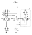
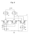
- a complementary tuned mixer circuit comprising; a first series circuit having a first pair of differentially arranged transistors receiving a first multiply signal in differential form, and an impedance circuit which operates as a constant current source; a second series circuit of the similar configuration to said first series circuit; a differential amplifier receiving a second multiply signal and providing a pair of outputs in differential form; said first series circuit and said second series circuit being inserted between a first power terminal (VDD) and a second power terminal, respectively through a respective load resistor (RL1, RL2); said differential amplifiers being supplied directly by said first power terminal (VDD), and each outputs in differential form being coupled with a junction of said impedance circuit and transistors in said first series circuit and a junction of said impedance circuit and transistors in said second series circuit, respectively; and a product, in differential form, of said first multiply signal and said second multiply signal being obtained at junction of said load resistors and said series circuits.
- the transistors composing said first series circuit and said second series circuit have opposite conductivity type to that of the transistors composing said differential amplifier.
- the voltage between a gate and a source in the first differential pair 1 and the second differential pair 2 is determined by the voltage between the local frequency signal (LO+, LO-) and the ground.
- Fig. 3 shows simulated waveforms of the device of Fig. 1, in which a computer program HSPICE was used.
- the power supply voltage VDD is 1 V
- the local frequency signal LO is 1.71 GHz
- the radio frequency signal RF is 1.95 GHz
- an output intermediate frequency is 240 MHz.
- a lowpass filter is used to process the intermediate frequency so that the difference frequency component (240 MHz) is clarified.
- a frequency mixer can operate with low voltage less than 1 V.
- the present invention uses a current source implemented by a parallel resonance circuit, instead of a current source implemented by a transistor in a prior art. Therefore, transistors are not connected in series between two power supply terminals.
- the circuit can operate with power supply voltage which is requested to operate one stage of a transistor, and therefore, the circuit can operate with low voltage around 1 V.
Landscapes
- Engineering & Computer Science (AREA)
- Power Engineering (AREA)
- Superheterodyne Receivers (AREA)
- Amplifiers (AREA)
Applications Claiming Priority (2)
| Application Number | Priority Date | Filing Date | Title |
|---|---|---|---|
| JP24001898 | 1998-08-26 | ||
| JP24001898 | 1998-08-26 |
Publications (2)
| Publication Number | Publication Date |
|---|---|
| EP0982848A1 true EP0982848A1 (de) | 2000-03-01 |
| EP0982848B1 EP0982848B1 (de) | 2002-10-30 |
Family
ID=17053249
Family Applications (1)
| Application Number | Title | Priority Date | Filing Date |
|---|---|---|---|
| EP99410102A Expired - Lifetime EP0982848B1 (de) | 1998-08-26 | 1999-08-24 | Abgestimmter komplementärer Mischer |
Country Status (3)
| Country | Link |
|---|---|
| US (1) | US6239645B1 (de) |
| EP (1) | EP0982848B1 (de) |
| DE (1) | DE69903702T2 (de) |
Cited By (3)
| Publication number | Priority date | Publication date | Assignee | Title |
|---|---|---|---|---|
| EP1133051A1 (de) * | 2000-03-08 | 2001-09-12 | Nippon Telegraph and Telephone Corporation | Mischerschaltung |
| FR2818828A1 (fr) * | 2000-12-22 | 2002-06-28 | St Microelectronics Sa | Disposition de transposition de frequence a haute admissibilite et faible dissipation |
| FR2827097A1 (fr) * | 2001-07-05 | 2003-01-10 | Zarlink Semiconductor Ltd | Dispositif de circuit melangeur et dispositif de circuit melangeur a rejection d'image |
Families Citing this family (17)
| Publication number | Priority date | Publication date | Assignee | Title |
|---|---|---|---|---|
| EP1111773B1 (de) * | 1999-06-29 | 2004-09-22 | Mitsubishi Denki Kabushiki Kaisha | Halbleiterschaltung |
| US7113744B1 (en) * | 1999-10-21 | 2006-09-26 | Broadcom Corporation | Adaptive radio transceiver with a power amplifier |
| US6388501B2 (en) * | 2000-04-17 | 2002-05-14 | Prominenet Communications Inc. | MOSFET mixer for low supply voltage |
| AU2003228602A1 (en) | 2002-04-22 | 2003-11-03 | Cognio, Inc. | Multiple-input multiple-output radio transceiver |
| US6959178B2 (en) * | 2002-04-22 | 2005-10-25 | Ipr Licensing Inc. | Tunable upconverter mixer with image rejection |
| JP2004072517A (ja) * | 2002-08-07 | 2004-03-04 | Alps Electric Co Ltd | ミキサ |
| DE10245609B4 (de) * | 2002-09-30 | 2014-01-02 | Advanced Micro Devices, Inc. | Mischvorrichtung |
| US6940352B2 (en) * | 2003-11-26 | 2005-09-06 | Scintera Networks, Inc. | Analog signal interpolation |
| KR100783492B1 (ko) * | 2004-07-31 | 2007-12-11 | 인티그런트 테크놀로지즈(주) | 차동증폭회로 및 이를 포함한 믹서회로 |
| JP4079953B2 (ja) * | 2005-02-17 | 2008-04-23 | 株式会社半導体理工学研究センター | 高周波回路 |
| US7577418B2 (en) * | 2006-07-18 | 2009-08-18 | United Microelectronics Corp. | Sub-harmonic mixer and down converter with the same |
| US7962114B2 (en) * | 2007-01-12 | 2011-06-14 | International Business Machines Corporation | Drain-pumped sub-harmonic mixer for millimeter wave applications |
| US8198933B2 (en) * | 2008-02-18 | 2012-06-12 | Freescale Semiconductor, Inc. | Mixer circuit |
| CN104052418A (zh) * | 2013-03-13 | 2014-09-17 | 华为技术有限公司 | 跨导电路和混频器 |
| US10622946B1 (en) | 2015-08-05 | 2020-04-14 | Sam Belkin | Frequency mixer |
| JP2017046246A (ja) * | 2015-08-27 | 2017-03-02 | 住友電気工業株式会社 | 電子回路 |
| US10855225B1 (en) * | 2019-12-23 | 2020-12-01 | Qualcomm Incorporated | Radio frequency low power differential frequency multiplier |
Citations (3)
| Publication number | Priority date | Publication date | Assignee | Title |
|---|---|---|---|---|
| EP0714163A1 (de) * | 1994-11-23 | 1996-05-29 | Analog Devices, Inc. | Mischer mit niedriger Versorgungsspannung |
| US5570056A (en) * | 1995-06-07 | 1996-10-29 | Pacific Communication Sciences, Inc. | Bipolar analog multipliers for low voltage applications |
| US5686870A (en) * | 1995-07-25 | 1997-11-11 | Murata Manufacturing Co., Ltd. | Mixer |
Family Cites Families (4)
| Publication number | Priority date | Publication date | Assignee | Title |
|---|---|---|---|---|
| JPH07131253A (ja) * | 1993-11-05 | 1995-05-19 | Fujitsu Ltd | 高周波乗算回路 |
| JP3097563B2 (ja) * | 1996-06-07 | 2000-10-10 | 日本電気株式会社 | 利得可変増幅器 |
| US5901350A (en) * | 1996-09-30 | 1999-05-04 | Fairchild Semiconductor Corporation | Low distortion large swing frequency down coverter filter amplifier circuit |
| US6094084A (en) * | 1998-09-04 | 2000-07-25 | Nortel Networks Corporation | Narrowband LC folded cascode structure |
-
1999
- 1999-08-24 DE DE69903702T patent/DE69903702T2/de not_active Expired - Lifetime
- 1999-08-24 EP EP99410102A patent/EP0982848B1/de not_active Expired - Lifetime
- 1999-08-24 US US09/382,123 patent/US6239645B1/en not_active Expired - Lifetime
Patent Citations (3)
| Publication number | Priority date | Publication date | Assignee | Title |
|---|---|---|---|---|
| EP0714163A1 (de) * | 1994-11-23 | 1996-05-29 | Analog Devices, Inc. | Mischer mit niedriger Versorgungsspannung |
| US5570056A (en) * | 1995-06-07 | 1996-10-29 | Pacific Communication Sciences, Inc. | Bipolar analog multipliers for low voltage applications |
| US5686870A (en) * | 1995-07-25 | 1997-11-11 | Murata Manufacturing Co., Ltd. | Mixer |
Non-Patent Citations (2)
| Title |
|---|
| HARUHIKO KOIZUMI ET AL: "A GAAS SINGLE BALANCED MIXER MMIC WITH BUILT-IN ACTIVE BALUN FOR PERSONAL COMMUNICATION SYSTEMS", IEEE MICROWAVE AND MILLIMETER-WAVE MONOLITHIC CIRCUITS SYMPOSIUM. MMWMC,US,NEW YORK, IEEE, pages 77-80, XP000538502, ISBN: 0-7803-2591-5 * |
| RAZAVI B: "A 1.5V 900MHZ DOWNCONVERTION MIXER", IEEE INTERNATIONAL SOLID STATE CIRCUITS CONFERENCE,US,IEEE INC. NEW YORK, vol. 39, pages 48-49, XP000685533, ISSN: 0193-6530 * |
Cited By (4)
| Publication number | Priority date | Publication date | Assignee | Title |
|---|---|---|---|---|
| EP1133051A1 (de) * | 2000-03-08 | 2001-09-12 | Nippon Telegraph and Telephone Corporation | Mischerschaltung |
| US6871057B2 (en) | 2000-03-08 | 2005-03-22 | Nippon Telegraph And Telephone Corporation | Mixer circuit |
| FR2818828A1 (fr) * | 2000-12-22 | 2002-06-28 | St Microelectronics Sa | Disposition de transposition de frequence a haute admissibilite et faible dissipation |
| FR2827097A1 (fr) * | 2001-07-05 | 2003-01-10 | Zarlink Semiconductor Ltd | Dispositif de circuit melangeur et dispositif de circuit melangeur a rejection d'image |
Also Published As
| Publication number | Publication date |
|---|---|
| EP0982848B1 (de) | 2002-10-30 |
| DE69903702D1 (de) | 2002-12-05 |
| DE69903702T2 (de) | 2003-07-03 |
| US6239645B1 (en) | 2001-05-29 |
Similar Documents
| Publication | Publication Date | Title |
|---|---|---|
| EP0982848B1 (de) | Abgestimmter komplementärer Mischer | |
| US6229395B1 (en) | Differential transconductance amplifier | |
| JP4308925B2 (ja) | 電流モード入力を備えた送信ミキサ | |
| US8933745B2 (en) | Transconductance-enhancing passive frequency mixer | |
| US7215201B2 (en) | Integrated circuit having a low power, gain-enhanced, low noise amplifying circuit | |
| EP1111773B1 (de) | Halbleiterschaltung | |
| JPH06188639A (ja) | 偶数項ミクサー | |
| US20030017816A1 (en) | Mixer circuit arrangement and an image-reject mixer circuit arrangement | |
| US6043710A (en) | Low-voltage amplifiers | |
| US6665527B2 (en) | Double balanced mixer circuit | |
| US5933057A (en) | Low noise amplifier | |
| US7176759B2 (en) | Differential low noise amplifier with low power consumption | |
| EP1142107B1 (de) | Aktiver differential asymmetrischer umwandler | |
| US6335651B1 (en) | Low voltage mixer | |
| EP1039629B1 (de) | Verstärkerschaltungsanordnung | |
| US6344762B1 (en) | Bias circuit for a low voltage differential circuit | |
| EP1378056B1 (de) | Verstärker-mischerschaltung | |
| US20090115515A1 (en) | Receiver Comprising an Amplifier | |
| EP1154567B1 (de) | Rundfunkfrequenzverstärker und Tuner | |
| JP3067772B2 (ja) | 相補型ミキサ回路 | |
| US7088184B2 (en) | High frequency amplifier in an integrated circuit | |
| JP2004166260A (ja) | ミキサ回路 | |
| US20060094389A1 (en) | Push-pull amplifier and frequency converter circuit | |
| HK1039837A (en) | Radio frequency amplifier and tuner | |
| US20040082307A1 (en) | Mixer circuit |
Legal Events
| Date | Code | Title | Description |
|---|---|---|---|
| PUAI | Public reference made under article 153(3) epc to a published international application that has entered the european phase |
Free format text: ORIGINAL CODE: 0009012 |
|
| AK | Designated contracting states |
Kind code of ref document: A1 Designated state(s): DE FR GB |
|
| AX | Request for extension of the european patent |
Free format text: AL;LT;LV;MK;RO;SI |
|
| 17P | Request for examination filed |
Effective date: 20000325 |
|
| AKX | Designation fees paid |
Free format text: DE FR GB |
|
| GRAG | Despatch of communication of intention to grant |
Free format text: ORIGINAL CODE: EPIDOS AGRA |
|
| 17Q | First examination report despatched |
Effective date: 20010614 |
|
| GRAG | Despatch of communication of intention to grant |
Free format text: ORIGINAL CODE: EPIDOS AGRA |
|
| GRAH | Despatch of communication of intention to grant a patent |
Free format text: ORIGINAL CODE: EPIDOS IGRA |
|
| GRAH | Despatch of communication of intention to grant a patent |
Free format text: ORIGINAL CODE: EPIDOS IGRA |
|
| GRAA | (expected) grant |
Free format text: ORIGINAL CODE: 0009210 |
|
| AK | Designated contracting states |
Kind code of ref document: B1 Designated state(s): DE FR GB |
|
| REG | Reference to a national code |
Ref country code: GB Ref legal event code: FG4D |
|
| REF | Corresponds to: |
Ref document number: 69903702 Country of ref document: DE Date of ref document: 20021205 |
|
| ET | Fr: translation filed | ||
| PLBE | No opposition filed within time limit |
Free format text: ORIGINAL CODE: 0009261 |
|
| STAA | Information on the status of an ep patent application or granted ep patent |
Free format text: STATUS: NO OPPOSITION FILED WITHIN TIME LIMIT |
|
| 26N | No opposition filed |
Effective date: 20030731 |
|
| PGFP | Annual fee paid to national office [announced via postgrant information from national office to epo] |
Ref country code: DE Payment date: 20140816 Year of fee payment: 16 |
|
| PGFP | Annual fee paid to national office [announced via postgrant information from national office to epo] |
Ref country code: GB Payment date: 20140820 Year of fee payment: 16 Ref country code: FR Payment date: 20140630 Year of fee payment: 16 |
|
| REG | Reference to a national code |
Ref country code: DE Ref legal event code: R082 Ref document number: 69903702 Country of ref document: DE |
|
| REG | Reference to a national code |
Ref country code: DE Ref legal event code: R119 Ref document number: 69903702 Country of ref document: DE |
|
| GBPC | Gb: european patent ceased through non-payment of renewal fee |
Effective date: 20150824 |
|
| REG | Reference to a national code |
Ref country code: FR Ref legal event code: ST Effective date: 20160429 |
|
| PG25 | Lapsed in a contracting state [announced via postgrant information from national office to epo] |
Ref country code: GB Free format text: LAPSE BECAUSE OF NON-PAYMENT OF DUE FEES Effective date: 20150824 Ref country code: DE Free format text: LAPSE BECAUSE OF NON-PAYMENT OF DUE FEES Effective date: 20160301 |
|
| PG25 | Lapsed in a contracting state [announced via postgrant information from national office to epo] |
Ref country code: FR Free format text: LAPSE BECAUSE OF NON-PAYMENT OF DUE FEES Effective date: 20150831 |