EP0982863B1 - Komparator and DA-Umsetzer mit geschalteten Kapazitäten - Google Patents
Komparator and DA-Umsetzer mit geschalteten Kapazitäten Download PDFInfo
- Publication number
- EP0982863B1 EP0982863B1 EP99202760A EP99202760A EP0982863B1 EP 0982863 B1 EP0982863 B1 EP 0982863B1 EP 99202760 A EP99202760 A EP 99202760A EP 99202760 A EP99202760 A EP 99202760A EP 0982863 B1 EP0982863 B1 EP 0982863B1
- Authority
- EP
- European Patent Office
- Prior art keywords
- input
- capacitor
- coupled
- voltage
- switch
- Prior art date
- Legal status (The legal status is an assumption and is not a legal conclusion. Google has not performed a legal analysis and makes no representation as to the accuracy of the status listed.)
- Expired - Lifetime
Links
- 239000003990 capacitor Substances 0.000 title claims abstract description 186
- 239000012071 phase Substances 0.000 claims description 36
- 238000000034 method Methods 0.000 claims description 17
- 239000012072 active phase Substances 0.000 claims description 8
- 238000004088 simulation Methods 0.000 description 9
- 230000008901 benefit Effects 0.000 description 7
- 238000010586 diagram Methods 0.000 description 7
- 238000006243 chemical reaction Methods 0.000 description 4
- 230000003321 amplification Effects 0.000 description 3
- 238000010276 construction Methods 0.000 description 3
- 238000004519 manufacturing process Methods 0.000 description 3
- 238000003199 nucleic acid amplification method Methods 0.000 description 3
- 238000002360 preparation method Methods 0.000 description 3
- 238000005070 sampling Methods 0.000 description 3
- 230000008878 coupling Effects 0.000 description 2
- 238000010168 coupling process Methods 0.000 description 2
- 238000005859 coupling reaction Methods 0.000 description 2
- 230000000694 effects Effects 0.000 description 2
- 230000006872 improvement Effects 0.000 description 2
- 238000012986 modification Methods 0.000 description 2
- 230000004048 modification Effects 0.000 description 2
- 230000004044 response Effects 0.000 description 2
- 230000009286 beneficial effect Effects 0.000 description 1
- 230000000295 complement effect Effects 0.000 description 1
- 230000001010 compromised effect Effects 0.000 description 1
- 239000013078 crystal Substances 0.000 description 1
- 230000001186 cumulative effect Effects 0.000 description 1
- 238000009826 distribution Methods 0.000 description 1
- 230000000977 initiatory effect Effects 0.000 description 1
- 238000002347 injection Methods 0.000 description 1
- 239000007924 injection Substances 0.000 description 1
- 238000005259 measurement Methods 0.000 description 1
- 230000001105 regulatory effect Effects 0.000 description 1
- 239000007787 solid Substances 0.000 description 1
- 230000006641 stabilisation Effects 0.000 description 1
- 238000011105 stabilization Methods 0.000 description 1
- 230000000087 stabilizing effect Effects 0.000 description 1
- 230000007704 transition Effects 0.000 description 1
Images



Classifications
-
- H—ELECTRICITY
- H03—ELECTRONIC CIRCUITRY
- H03M—CODING; DECODING; CODE CONVERSION IN GENERAL
- H03M1/00—Analogue/digital conversion; Digital/analogue conversion
- H03M1/12—Analogue/digital converters
- H03M1/14—Conversion in steps with each step involving the same or a different conversion means and delivering more than one bit
- H03M1/16—Conversion in steps with each step involving the same or a different conversion means and delivering more than one bit with scale factor modification, i.e. by changing the amplification between the steps
- H03M1/164—Conversion in steps with each step involving the same or a different conversion means and delivering more than one bit with scale factor modification, i.e. by changing the amplification between the steps the steps being performed sequentially in series-connected stages
- H03M1/167—Conversion in steps with each step involving the same or a different conversion means and delivering more than one bit with scale factor modification, i.e. by changing the amplification between the steps the steps being performed sequentially in series-connected stages all stages comprising simultaneous converters
- H03M1/168—Conversion in steps with each step involving the same or a different conversion means and delivering more than one bit with scale factor modification, i.e. by changing the amplification between the steps the steps being performed sequentially in series-connected stages all stages comprising simultaneous converters and delivering the same number of bits
-
- H—ELECTRICITY
- H03—ELECTRONIC CIRCUITRY
- H03K—PULSE TECHNIQUE
- H03K5/00—Manipulating of pulses not covered by one of the other main groups of this subclass
- H03K5/22—Circuits having more than one input and one output for comparing pulses or pulse trains with each other according to input signal characteristics, e.g. slope, integral
- H03K5/24—Circuits having more than one input and one output for comparing pulses or pulse trains with each other according to input signal characteristics, e.g. slope, integral the characteristic being amplitude
- H03K5/2472—Circuits having more than one input and one output for comparing pulses or pulse trains with each other according to input signal characteristics, e.g. slope, integral the characteristic being amplitude using field effect transistors
- H03K5/2481—Circuits having more than one input and one output for comparing pulses or pulse trains with each other according to input signal characteristics, e.g. slope, integral the characteristic being amplitude using field effect transistors with at least one differential stage
-
- H—ELECTRICITY
- H03—ELECTRONIC CIRCUITRY
- H03K—PULSE TECHNIQUE
- H03K5/00—Manipulating of pulses not covered by one of the other main groups of this subclass
- H03K5/22—Circuits having more than one input and one output for comparing pulses or pulse trains with each other according to input signal characteristics, e.g. slope, integral
- H03K5/24—Circuits having more than one input and one output for comparing pulses or pulse trains with each other according to input signal characteristics, e.g. slope, integral the characteristic being amplitude
- H03K5/2472—Circuits having more than one input and one output for comparing pulses or pulse trains with each other according to input signal characteristics, e.g. slope, integral the characteristic being amplitude using field effect transistors
- H03K5/249—Circuits having more than one input and one output for comparing pulses or pulse trains with each other according to input signal characteristics, e.g. slope, integral the characteristic being amplitude using field effect transistors using clock signals
Definitions
- the present invention relates generally to the field of analog circuitry, and is more specifically directed to switched-capacitor circuits.
- switched-capacitor techniques are utilized in many applications.
- switched-capacitor circuits operate by periodically connecting an input voltage to a capacitor, which in turn stores a charge corresponding to the applied voltage.
- the capacitor is subsequently connected to an input of an amplifier or other circuit to communicate the input voltage to downstream circuitry.
- sample-and-hold functions are commonly realized by way of switched-capacitor techniques.
- switched-capacitor techniques are comparison of an input signal voltage to a reference voltage.
- the sampling capacitor is initially connected to a reference voltage, such as may be generated by a band-gap voltage reference circuit or similar circuit for generating a reference voltage that is relatively stable over variations in power supply voltage, temperature, and manufacturing process parameters.
- the capacitor is then switchably connected to receive a signal input voltage, such that the resulting charge on the capacitor corresponds to the differential between the signal input voltage and the reference voltage. This resulting charge can then be sensed by an amplifier, which in turn generates a signal corresponding to that differential.
- the reference voltage is then again connected to the sampling capacitor in preparation for the next sample of the input voltage.
- ADC 10 receives an analog input voltage on line V IN and generates, at its output, an n-bit digital word on lines V OUT that correspond to the input analog voltage.
- ADC 10 includes a series of analog stages 4 0 through 4 k .
- First stage 4 0 receives the analog input voltage on line V IN and, based on the amplitude of this input voltage, generates an m-bit digital output on lines Do and a residue output on lines RES 0 .
- the number of digital bits m generated by each stage 4 is 2 or more.
- the residue voltage on line RES 0 corresponds to a remainder of the "division" carried out in the digitization operation.
- each subsequent, lower-order, stage 4 j receives the residue voltage on lines RES j-1 from the previous stage 4 j-1 , and similarly generates m digital output bits on lines Dj, and a residue analog voltage on line RESj that is forwarded to the next stage 4 j+1 in the pipeline.
- each stage 4 j are stored in corresponding latch 6 j , the contents of which are summed, by adder 8 j , with the digital result on lines D j+1 from the next stage 4 j+1 in the sequence; the output of the final adder 8 k is the n-bit digital output word on lines V OUT .
- the pipelining effect of ADC 10 is enabled by the operation of latches 6; once a stage 4 j derives a digital result and residue, it can begin conversion of the next sample in time while the next stage 4 j+1 operates on the result from the previous sample.
- each of the multiple stages 4 in ADC 10 can be operating on different samples of the input signal voltage V IN , with a sequence of digital results generated by final adder 8 k .
- Figure 2 illustrates the functional construction of exemplary analog stage 4 j in ADC 10 of Figure 1.
- input voltage V in is applied to sub-ADC 5, which produces the digital output on lines D j ; these digital outputs are also applied to sub-DAC 7, which presents an analog signal to subtractor 9.
- Subtractor 9 subtracts the output from sub-DAC 7 from the value of input voltage V in , sampled and held by sample-and-hold circuit 3; the output of subtractor 9 is amplified by gain amplifier 11 to generate analog residue voltage on line RESj that is within a voltage range suitable for use by a next, downstream, analog stage 4 j+1 .
- each of nine stages receives two reference voltage levels at switched-capacitor inputs.
- switched-capacitor pipelined ADC circuits provide excellent resolution at extremely high conversion rates, considering the pipelined architecture of the ADC.
- each switched-capacitor stage of the ADC performs a comparison of sampled differential input voltages, precharging sample nodes to reference voltages before each sample of the differential input signal.
- Accuracy in this comparison requires, of course, reference voltages that are not only stable over variations in power supply voltage, temperature, and manufacturing process parameters, but is also stable considering the switching operation of the ADC.
- FIG 3 illustrates an example of conventional differential switched-capacitor stage 15 j as may be used in modern pipelined ADCs and other circuits that utilize switched-capacitor comparisons.
- switched-capacitor stage 15 j receives a differential input voltage on lines V in + and V in - , and two reference voltage levels V refp and V refn .
- switched-capacitor stage 15 j compares the voltage on line V in + with the voltage on line V in - , after precharging respective capacitor inputs to reference voltages V refp , V refn .
- Reference voltages V refp and V refn are generated by reference voltage circuit 20 which includes, in this conventional example, bandgap circuit 12 for generating a voltage on line V r that is stable over variations in power supply voltage, temperature, and manufacturing process parameters.
- bandgap circuit 12 for generating a voltage on line V r that is stable over variations in power supply voltage, temperature, and manufacturing process parameters.
- bandgap circuit 12 are well known in the art.
- Line V r in this example, is applied to an inverting input of operational amplifier 14, which has its non-inverting input biased to ground.
- Switched-capacitor stage 15j includes a differential operational amplifier 16 which, as will now be described, generates a differential voltage on lines V out + and V out - in response to a switched-capacitor comparison of the voltages on lines V in + and V in - .
- input voltage V in + is coupled to node V A at sample-and-hold capacitor CIN+ by way of switch 17+, and is coupled to feedback capacitor CFB+ by way of switch 18+.
- switches 17+, 18+, as well as the other switches 17, 18, 19, 21 in switched-capacitor stage 15 j are conventional passgates, such as n-channel MOS transistors, or parallel CMOS transistors receiving complementary signals at their gates, as well known in the art.
- each of switches 17+, 18+ are controlled by clock ⁇ 1 , which is the sample clock in this arrangement.
- Reference voltage V refp is coupled to node V A at sample-and-hold capacitor CIN+ by way of switch 19+, which is controlled by amplify clock ⁇ 2 .
- Clock ⁇ 2 also controls, via switch 21+, the coupling of feedback from the non-inverting output of amplifier 16 to the inverting input thereof through feedback capacitor CFB+.
- the inverting input of amplifier 16 is connected to sample-and-hold capacitor CIN-, the opposite plate of which is coupled, at node V B , to input voltage V in - through switch 19-, and to reference voltage V refn through switch 19-.
- the inverting input of amplifier 16 is also connected to one plate of feedback capacitor CFB-.
- the opposite plate of feedback capacitor CFB- is coupled to input voltage V in - via switch 18- and, through switch 21-, to line V out - at the inverting output of amplifier 16.
- Switches 17- and 18- are controlled by sample clock ⁇ 1 while switches 19- and 21- are controlled by amplify clock ⁇ 2 .
- Sample clock ⁇ 1 and amplify clock ⁇ 2 are non-overlapping clock phases of the same frequency.
- sampling is effected by switched-capacitor stage 15 j upon sample clock ⁇ 1 being driven active (amplify clock ⁇ 2 inactive at this time); during this phase, nodes V A , V B receive input voltages V in + , V in - , through switches 17+, 17-, respectively; these input voltages V in + , V in - are also respectively applied to feedback capacitors CFB+, CFB- through switches 18+, 18-.
- switches 21+, 21- apply feedback from output lines V out + , V out - , respectively, to their respective feedback capacitors CFB+, CFB, so that amplification is carried out by amplifier 16 according to the appropriate desired characteristics.
- reference voltages V refp , V refn are applied to nodes V A , V B , respectively, through respective switches 19+, 19- during this active phase of amplify clock ⁇ 2 , such that the next samples of input voltages V in + , V in - are accurately obtained (and their differential accurately compared against the reference voltage differential V refp -V refn ), independently from the voltage of the prior sample.
- the operation then repeats, in the next cycles of sample clock ⁇ 1 and amplify clock ⁇ 2 , to obtain and amplify the next sample of input voltages V in + , V in - .
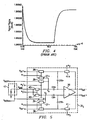
- switched-capacitor circuits such as switched-capacitor stage 15 j of Figure 3, present substantial load upon the reference voltages generated by reference voltage circuit 20 of Figure 3.
- This load is, of course, exacerbated in circuits such as pipelined ADCs, where multiple switched-capacitor stages (up to sixteen such stages, in typical high-resolution ADC examples) receive the reference voltages and simultaneously switch their inputs. Because of this load, and the switching operations that such conventional circuits perform, the stability of the reference voltage can be compromised.
- This operation corresponds to the largest capacitor voltage swings at sample-and-hold capacitors CIN+, CIN-.
- new samples are obtained with input voltage V in + set equal to reference voltage V refp , and input voltage V in - set equal to reference voltage V refn .
- this simulation reverted the input voltages to their initial state, with input voltage V in + set equal to reference voltage V refn , and input voltage V in - set equal to reference voltage V refp .
- the actual reference voltage differential V refp -V refn will, in practice, vary within these worst case limits of Figure 4.
- the reference voltage differential V refp -V refn varies according to the value of the input voltages V in + , V in - , due to the loading presented by switched-capacitor stage 15 j , and the charge sharing between sample-and-hold capacitors CIN+, CIN- and the capacitors in reference voltage circuit 20.
- This dependence on input voltage is, of course, undesirable in applications such as ADCs, where accuracy in measurement of the input voltage is of highest importance. While variations of on the order of 90 microvolts are within the tolerance of some applications, such variations are not acceptable for high precision ADCs; indeed, the stability of reference voltages can limit the precision (i.e., number of bits) of the ADC itself. Conversely, improved stability of reference voltages can enable the construction and accurate operation of ADC circuits with additional bits of precision.
- the teachings of the present application disclose a switched-capacitor circuit that presents reduced switching load to the reference voltages applied thereto.
- the teachings further disclose a circuit that may be readily implemented in switched-capacitor circuits with minimal overhead.
- the teachings yet further disclose a pipelined ADC including multiple ones of such switched-capacitor circuits, such an ADC having improved precision over conventional ADC circuits.
- the apparatus and method disclosed by the teachings of the present application may be implemented in a switched-capacitor circuit having an amplifier with at least one input coupled, by way of a sample-and-hold capacitor, to switches through which an input voltage and a reference voltage are applied in non-overlapping sample and reference clock phases, respectively.
- the circuit also includes another switch through which a midlevel voltage is applied to the sample-and-hold capacitor during a third non-overlapping phase between the sample and reference clock phases.
- the application of the midlevel voltage limits the worst case loading presented to the reference voltage, thus limiting variations in the reference voltage as a result of input switching.
- the reduced reference voltage variations enable additional bits of precision in the analog-to-digital conversion.
- Figure 1 is an electrical diagram, in block form, of a conventional pipelined analog-to-digital converter (ADC).
- ADC analog-to-digital converter
- Figure 2 is an electrical diagram, in block form, of a conventional stage in the pipelined ADC of Figure 1.
- Figure 3 is an electrical diagram, in schematic form, of a conventional differential switched-capacitor stage, and accompanying voltage reference circuit, such as used in the conventional pipelined ADC of Figure 1.
- Figure 4 is a voltage plot over time of a simulation of the operation of the differential switched-capacitor stage of Figure 3.
- Figure 5 is an electrical diagram, in schematic form, of a differential switched-capacitor stage.
- Figure 6 is a timing diagram illustrating the operation of the differential switched-capacitor stage of Figure 5, constructed.
- Figure 7 is a voltage plot over time of a simulation of the operation of the differential switched-capacitor stage of Figure 5.
- Figure 8 is an electrical diagram, in block form, of a pipelined ADC incorporating the differential switched-capacitor stage of Figure 5.
- the present invention may be implemented according to many alternative realizations and applications.
- a preferred embodiment will be described hereinbelow relative to a differential switched-capacitor circuit, it is contemplated that the present invention may be realized in switched-capacitor circuits having single-ended inputs.
- the present invention is of particular benefit in circuits having several to many switched-capacitors stages, such circuits including pipelined analog-to-digital converters (ADCs), other applications of the present invention may also benefit from the present invention. It is therefore contemplated that such alternative realizations and applications will be within the scope of the present invention, as claimed hereinbelow.
- differential switched-capacitor stage 35 j includes differential operational amplifier 36, having inverting and non-inverting inputs, and inverting and non-inverting outputs, and which is capacitively coupled to input voltages (and with capacitive feedback) so as to operate as a differential sample-and-hold amplifying circuit stage.
- the non-inverting input of amplifier 36 is connected to one plate of sample-and-hold capacitor CIN+, and to one plate of feedback capacitor CFB+.
- the opposite plate of sample-and-hold capacitor CIN+ at node V A is coupled to input voltage V in + through switch 37+, and to reference voltage V refp through switch 39+.
- the plate of feedback capacitor CFB+ opposite that of the non-inverting input of amplifier 36 is coupled to input voltage V in + through switch 38+, and to the non-inverting output of amplifier 36 at line V out - through switch 41+.
- Switches 37+, 38+, 39+, 41+ are all implemented as conventional passgates (e.g., CMOS or NMOS passgates).
- switches 37+, 38+ are controlled by sample clock ⁇ 1
- switch 41+ is controlled by amplify clock ⁇ 2
- switch 39+ is controlled by reference voltage clock ⁇ 2 " which, as will be described in detail below, is driven active during a latter portion of the active phase of amplify clock ⁇ 2 .
- the inverting input of amplifier 36 is similarly connected to one plate of sample-and-hold capacitor CIN-, and to one plate of feedback capacitor CFB-.
- the opposite plate of sample-and-hold capacitor CIN- at node V B is coupled to input voltage V in - through switch 37-, and to reference voltage V refn through switch 39-, while the opposite plate of feedback capacitor CFB- is coupled to input voltage V in - through switch 38-, and to the inverting output of amplifier 36 at line V out + through switch 41-.
- switches 37+, 38+, 39+, 41+, switches 37-, 38-; 39-, 41- are all conventional passgates, implemented either as single transistors are as CMOS passgates.
- switches 37+, 38+, 39+, 41+ are controlled by sample clock ⁇ 1
- switch 39- is controlled by reference clock ⁇ 2 "
- switch 41- is controlled by amplify clock ⁇ 2 .
- reference voltages V refp , V refn define the extremes of the voltage range over which the input voltages V in + , V in - may vary.
- reference voltage V refp will be at approximately 2.5 volts
- reference voltage V refn will be at approximately 0.5 volts.
- the particular voltage range of input voltages V in + , V in - and reference voltages V refp , V refn will vary according to the particular application.
- nodes V A and V B are each also coupled to a third voltage V mid , by way of switches 40+, 40-, respectively.
- Voltage V mid is preferably a voltage at a level between reference voltages V refp , V refn ; however, this voltage V mid may be unregulated, as its specific level is not critical to operation.
- voltage divider 42 is provided to generate voltage V mid from reference voltages V refp , V refn themselves, by way of a conventional resistor divider connected in series between reference voltages V refp , V refn , with a stabilizing capacitor connected between its output and ground.
- voltage V mid may be generated from a voltage division of power supply voltage V dd and ground, or as a third reference voltage from a voltage generator circuit as known in the art. As will become apparent from the following description, however, the actual level of voltage V mid need not be is not critical, and as such need not be precisely generated or regulated.
- voltage V mid is selected to be about the midlevel voltage between the reference voltage received at a particular input, and the opposite extreme of the input signal applied to that same input.
- voltage V mid may be selected to a voltage that is approximately midway between the extremes of the range of input voltages V in + , V in - , these extremes defined by reference voltages V refp , V refn .
- input voltages V in + , V in - may vary from 0.5 volts to 2.5 volts
- voltage V mid is preferably at about 1.5 volts.
- V midlevel V mid will vary according to the particular application, and according to the particular voltages utilized therein. Further in the alternative, it is contemplated, in the differential switched-capacitor case such as described relative to Figure 5, that the application of different voltages V mid + , V mid - to the differential sample nodes V A , V B may be beneficial.
- Switches 40+, 40- are each controlled by precharge clock ⁇ 2 '.
- precharge clock ⁇ 2 ' is driven active during an early portion of the active phase of amplify clock ⁇ 2 .
- both node V A and also node V B receive the voltage on line V mid .
- the active phase of precharge clock ⁇ 2 ' does not overlap either of the active phases of sample clock ⁇ 1 or reference clock ⁇ 2 '', and preferably occurs, in each cycle, after the active phase of sample clock ⁇ 1 and during an initial portion of the active phase of amplify clock ⁇ 2 .
- the duration of the active phase of precharge clock ⁇ 2 ' need not be selected or maintained with a high degree of precision.
- an active phase of sample clock ⁇ 1 begins.
- switches 37+, 37-, 38+, 38- in switched-capacitor stage 35 j are closed, thus applying input voltage V in + to node V A at sample capacitor CIN+ and input voltage V in - to node V B at sample capacitor CIN-.
- input voltages V in + , V in - are applied to feedback capacitors CFB+, CFB-, respectively, through respective switches 38+, 38-.
- nodes V A , V B discharge and charge, respectively, toward their respective input voltages V in + , V in - after time to, reaching the level of these input voltages during the active phase of sample clock ⁇ 1 .
- amplifier 36 begins generating its output at lines V out - , V out + , based on the samples of the input voltages obtained at its inputs via capacitors CIN+, CIN-.
- the active phase of sample clock ⁇ 1 ends shortly prior to time t 1 in the example of Figure 6, responsive to which switches 37+, 38+, 37-, 38- open.
- amplify clock ⁇ 2 and precharge clock ⁇ 2 ' begin active phases at time t 1 .
- the active phase amplify clock ⁇ 2 effects amplification via amplifier 36, while the active phase of precharge clock ⁇ 2 ' prepares switched-capacitor stage 35 j for the next cycle.
- the active phase of amplify clock ⁇ 2 closes switches 41+, 41-, so that feedback from output lines V out - , V out + are respectively applied to feedback capacitors CFB+, CFB-.
- amplifier 36 continues its amplification operation, generating the appropriate differential voltage at output lines V out - , V out + according to the sampled differential input voltages V in + , V in - and according to the negative feedback applied via feedback capacitors CFB+, CFB-.
- precharge clock ⁇ 2 ' at time t 1 closes switches 40+, 40-, such that voltage V mid , which in this case is generated by voltage divider 42, is applied to nodes V A , V B .
- voltage V mid which in this case is generated by voltage divider 42
- the voltages at nodes V A , V B charge and discharge, respectively, toward voltage V mid .
- the duration PW of the active pulse of precharge clock ⁇ 3 may be quite short, for example on the order of 10 nsec for a 5 MHz application, considering that it is not essential that nodes V A , V B actually reach voltage V mid in order to provide the benefits of the present invention.
- reference clock ⁇ 2 enters its active phase, closing switches 39+, 39- to apply reference voltages V refp , V refn to nodes V A , V B , respectively.
- This closing of switches 39+, 39- charges and discharges nodes V A , V B to reference voltages V refp , V refn , respectively, in preparation for the next cycle.
- both amplify clock ⁇ 2 and reference clock ⁇ 2 " return to an inactive state, prior to initiation of the next sample cycle.
- precharge clock ⁇ 2 ' in applying voltage V mid to sample nodes V A , V B will result in significant improvement in the stability of reference voltages V refp , V refn over time, primarily by presenting a constant impedance to the circuitry generating the reference voltages. This improvement may be explained by consideration of the distribution of charge between the reference voltage circuit and the sample capacitors of the switched-capacitor stages, as will now be described.
- Conventional reference voltage circuits include large capacitors at their outputs, relative to the sample capacitors V A , V B of switched-capacitor stages 35. For a given reference voltage V ref , one may thus consider a total charge Q TOT as the sum of the charge on the corresponding voltage reference capacitor of capacitance C ref plus the charge on the sample capacitor of capacitance C sample . Of course, the charge on a capacitor is simply the product of the capacitance of the capacitor with the voltage thereacross.
- the present invention is directed to eliminating the variations of the reference voltage by ensuring that sample capacitors CIN+, CIN- are at the same voltage, in each cycle, immediately prior to the application of reference voltages V refp , V refn thereto. As described above, this is accomplished by way of switches 40+, 40- which apply voltage V mid to sample nodes V A , V B during the active phase of precharge clock ⁇ 2 ', prior to the active phase of reference clock ⁇ 2 '' as shown in Figure 6.
- the reference voltage differential V refp -V refn remains stable once it has settled.
- the reference voltage differential V refp -V refn remains at this lower voltage despite this switching operation, because of the application of voltage V mid to sample nodes V A , V B as described above.
- FIG 8 illustrates pipelined ADC 50, constructed according to the preferred embodiment of the present invention and as such including a series of switched-capacitor stages 35 0 through 35 k , constructed as described hereinabove relative to Figure 5.
- switched-capacitor stages 35 are all associated with a digital latch and adder circuitry 44, which carries out the necessary digitization of the results of the switched-capacitor stages 35.
- switched-capacitor stage 35 0 receives a differential voltage on lines V IN + and V IN - .
- switched-capacitor stage 35 0 In response, switched-capacitor stage 35 0 generates output that is applied to digital latch and adder circuitry 44; switched-capacitor stage 35 0 also generates a differential residue signal on lines RES 0 , which corresponds to an analog remainder from the digitization operation for this stage, amplified to voltage levels suitable for operation by the next combination of switched-capacitor stage 35 1 to which lines RES 0 are applied as shown in Figure 8.
- Switched-capacitor stage 35 1 then, in turn, generates a digital output that is applied to digital latch and adder circuitry 44, along with a residue signal on lines RES 1 for application to the next stage 35 2 (not shown).
- This sequence of stages 35 continues, as shown in Figure 8, through k th switched-capacitor stage 35 k ; switched-capacitor stage 35 k produces no residue signal, as no further stages are present in ADC 50.
- Digital latch and adder circuitry 44 produces, in a pipelined fashion, a digital output of pipelined ADC 50 on bus DATA OUT.
- n-bit precision where n may be 14, 16, or higher
- the number k+1 of switched-capacitor stages 35 can number up to as many as n-1 (i.e., fifteen or more such stages 35).
- Clock generation circuitry 60 is also provided in pipelined ADC 50 according to a preferred embodiment disclosed by the present teachings, and is constructed according to conventional clock circuit techniques to generate, from an external clock signal or crystal oscillator connected to line CLIN, non-overlapping phases of sample clock ⁇ 1 , amplify clock ⁇ 2 , precharge clock ⁇ 2 ', and reference clock ⁇ 2 '' for application to each of switched-capacitor stages 35 0 through 35 k .
- the relative timing of the active phases of sample clock ⁇ 1 , amplify clock ⁇ 2 , precharge clock ⁇ 2 ', and reference clock ⁇ 2 '' correspond to that described above relative to Figure 6.
- pipelined ADC 50 includes voltage reference circuit 20, which may be constructed in the manner described hereinabove relative to Figure 3.
- Voltage reference circuit 20 generates reference voltages V refp , V refn and applies these voltages, in parallel, to each of switched-capacitor stages 35 0 through 35 k .
- Voltage reference circuit 20 also applies reference voltages V refp , V refn to voltage divider 42, which in turn generates voltage V mid that is applied to each of switched-capacitor stages 35 0 through 35 k .
- voltage reference circuit 20 is presented with a cumulative load due to the switching at the respective sample-and-hold capacitors CIN+, CIN- of each switched-capacitor stages 35 0 through 35 k .
- each of switched-capacitor stages 35 0 through 35 k applies voltage V mid to its sample-and-hold capacitors CIN+, CIN- under the control of precharge clock ⁇ 2 '
- a constant impedance is presented to voltage reference circuit 20 over time, resulting in much improved stability of reference voltages V refp , V refn over the switching operation of ADC 50.
- This improved stability enables the implementation of additional bits of precision in the analog-to-digital conversion by way of pipelined ADCs, and thus additional usability of digital techniques for processing of analog signals.
- ADC 50 many circuit applications of the apparatus and method disclosed by the present application such as ADC 50 will implement several to many switched-capacitor stages, each of which utilize reference voltages generated from an on-chip reference voltage circuit. In the operation of such applications, it is contemplated that the stabilization of reference voltages may require many cycles.
- the simulation of switched-capacitor stage 35 j arranged according to a preferred embodiment disclosed by the present teachings has determined that the reference voltages applied thereto can stabilize, after operation for 40 cycles, to an accuracy of less than 10 microvolts.
- the actual reference voltage stability has been found to depend upon the latency that can be afforded in executing the sample, hold, and amplify operations.
- high-resolution pipelined ADCs such as the example of ADC 50 described above, generally require many cycles for proper operation, such latency can often be afforded, especially with improved precision as a benefit.
- switched-capacitor circuits may be constructed to operate at relatively high frequencies, but with minimal loading upon reference voltages applied thereto, such that the stability of the reference voltage is greatly improved, even in integrated circuits in which several to many switched-capacitor circuits each receive the reference voltages, and are simultaneously switched.
- the disclosed apparatus and method is thus contemplated to provide important benefits, particularly in enabling precision functionality of modern high performance circuits, such as pipelined analog-to-digital converters.
Landscapes
- Physics & Mathematics (AREA)
- Nonlinear Science (AREA)
- Engineering & Computer Science (AREA)
- Theoretical Computer Science (AREA)
- Analogue/Digital Conversion (AREA)
- Amplifiers (AREA)
- Filters That Use Time-Delay Elements (AREA)
- Measurement Of Current Or Voltage (AREA)
Claims (20)
- Schaltkreis mit geschalteten Kapazitäten, umfassend:einen Verstärker (36) mit einem ersten Eingang und einem ersten Ausgang;einen ersten Abtastkondensator (Cin), der einen ersten Belag mit dem ersten Eingang des Verstärkers gekoppelt hat, und der einen zweiten Belag an einem ersten Abtastknoten (Va, Vb) hat;einen ersten Signaleingangsschalter (38), gekoppelt zwischen einem ersten Signaleingang und dem ersten Abtastknoten, wobei der erste Signaleingangsschalter gekoppelt ist, um ein erstes Taktsignal (Φ1) zu empfangen;einen ersten Referenzeingangsschalter (39), gekoppelt zwischen einem ersten Referenzspannungseingang (Vrefp, Vrefn) und dem ersten Abtastknoten (Va, Vb), wobei der erste Referenzeingangsschalter gekoppelt ist, um ein zweites Taktsignal (Φ2'') zu empfangen;einen ersten Vorladeschalter (40), gekoppelt zwischen einer Vorladespannung (Vmid) und dem ersten Abtastknoten (Va, Vb), wobei der erste Vorladeschalter gekoppelt ist, um ein Vorladetaktsignal (Φ2') zu empfangen; undein erstes Rückkopplungsnetzwerk (CFB), gekoppelt zwischen dem ersten Ausgang (Vout) des Verstärkers (36) und dem ersten Eingang des Verstärkers.
- Schaltkreis mit geschalteten Kapazitäten aus Anspruch 1, ferner umfassend:eine Spannungsreferenzschaltung zur Erzeugung der ersten Referenzspannung (Vrefp, Vrefn).
- Schaltkreis mit geschalteten Kapazitäten aus Anspruch 2, bei dem die erste Eingangsspannung (Vin) innerhalb eines Spannungsbereichs zwischen ersten und zweiten Extremwerten variiert;
bei dem die erste Referenzspannung bei einer Spannung nahe des ersten Extremwerts des Spannungsbereichs liegt;
und ferner umfassend:eine Vorladespannungs- (Vmid-) Erzeugungsschaltung zur Erzeugung der Vorladespannung bei einer Spannung, die sich ungefähr in der Mitte zwischen der ersten Referenzspannung und dem zweiten Extremwert des Eingangsspannungsbereichs befindet. - Schaltkreis mit geschalteten Kapazitäten aus Anspruch 1, ferner umfassend:eine Taktgeneratorschaltung zur Erzeugung des ersten (Φ1) und des zweiten Taktsignals (Φ2'') und des Vorladetaktsignals (Φ2') derart, dass sich aktive Phasen des ersten und des zweiten Taktsignals und des Vorladetaktsignals zeitlich nicht gegenseitig überschneiden.
- Schaltkreis mit geschalteten Kapazitäten aus Anspruch 1, bei dem das erste Rückkopplungsnetzwerk Folgendes umfasst:einen ersten Rückkopplungskondensator (CFB) mit einem ersten Belag, der mit dem ersten Eingang des Verstärkers gekoppelt ist, und mit einem zweiten Belag;einen ersten Referenzrückkopplungsschalter (38), gekoppelt zwischen dem ersten Referenzspannungseingang und dem zweiten Belag des Rückkopplungskondensators (CFB), und durch das erste Taktsignal (Φ1) gesteuert; undeinen ersten Ausgangsrückkopplungsschalter (41), gekoppelt zwischen dem ersten Ausgang des Verstärkers (36) und dem zweiten Belag des Rückkopplungskondensators, und durch ein Verstärkungstaktsignal (Φ2) gesteuert.
- Schaltkreis mit geschalteten Kapazitäten aus Anspruch 1, bei dem der Verstärker (36) auch einen zweiten Eingang und einen zweiten Ausgang hat, wobei der erste und der zweite Eingang des Verstärkers einem Differenzeingang entsprechen, und der erste und der zweite Ausgang des Verstärkers einem Differenzausgang entsprechen;
und ferner umfassend:einen zweiten Abtastkondensator (CFB-) mit einem ersten Belag, der mit dem zweiten Eingang des Verstärkers gekoppelt ist, und mit einem zweiten Belag an einem zweiten Abtastknoten (Vb);einen zweiten Signaleingangsschalter (38-), gekoppelt zwischen einem zweiten Signaleingang und dem zweiten Abtastknoten, wobei der zweite Signaleingangsschalter gekoppelt ist, um das erste Taktsignal (Φ1) zu empfangen;einen zweiten Referenzeingangsschalter (39-), gekoppelt zwischen einem zweiten Referenzspannungseingang (Vrefn) und dem zweiten Abtastknoten (Vb), wobei der zweite Referenzeingangsschalter gekoppelt ist, um das zweite Taktsignal zu empfangen; undeinen zweiten Vorladeschalter (40-), gekoppelt zwischen einer Vorladespannung (Vmid) und dem Abtastknoten, wobei der zweite Vorladeschalter gekoppelt ist, um das Vorladetaktsignal (Φ2') zu empfangen. - Schaltkreis mit geschalteten Kapazitäten aus Anspruch 6, bei dem der erste (40+) und der zweite (40-) Vorladeschalter mit derselben Vorladespannung (Vmid) gekoppelt sind.
- Schaltkreis mit geschalteten Kapazitäten aus Anspruch 6, ferner umfassend:eine Spannungsreferenzschaltung zur Erzeugung der ersten (Vrefp) und der zweiten (Vrefn) Referenzspannung.
- Schaltkreis mit geschalteten Kapazitäten aus Anspruch 8, ferner umfassend:eine Vorladespannungs-Erzeugungsschaltung (42) zur Erzeugung der Vorladespannung bei einer Spannung, die sich ungefähr in der Mitte zwischen der ersten (Vrefp) und der zweiten Referenzspannung (Vrefn) befindet.
- Schaltkreis mit geschalteten Kapazitäten aus Anspruch 6, ferner umfassend:eine Taktgeneratorschaltung zur Erzeugung des ersten (Φ1) und des zweiten Taktsignals (Φ2'') und des Vorladetaktsignals (Φ2') derart, dass sich aktive Phasen des ersten und des zweiten Taktsignals und des Vorladetaktsignals zeitlich nicht gegenseitig überschneiden.
- Schaltkreis mit geschalteten Kapazitäten aus Anspruch 6, bei dem das erste Rückkopplungsnetzwerk Folgendes umfasst:einen ersten Rückkopplungskondensator (CFB) mit einem ersten Belag, der mit dem ersten Eingang des Verstärkers (36) gekoppelt ist, und mit einem zweiten Belag;einen ersten Referenzrückkopplungsschalter (38+), gekoppelt zwischen dem ersten Referenzspannungseingang und dem zweiten Belag des ersten Rückkopplungskondensators, und durch das erste Taktsignal gesteuert; undeinen ersten Ausgangsrückkopplungsschalter (41+), gekoppelt zwischen dem ersten Ausgang des Verstärkers und dem zweiten Belag des ersten Rückkopplungskondensators, und durch ein Verstärkungstaktsignal gesteuert;und bei dem das zweite Rückkopplungsnetzwerk Folgendes umfasst:einen zweiten Rückkopplungskondensator (CFB-) mit einem ersten Belag, der mit dem zweiten Eingang des Verstärkers gekoppelt ist, und mit einem zweiten Belag;einen zweiten Referenzrückkopplungsschalter (38-), gekoppelt zwischen dem zweiten Referenzspannungseingang und dem zweiten Belag des zweiten Rückkopplungskondensators, und durch das erste Taktsignal gesteuert; undeinen zweiten Ausgangsrückkopplungsschalter (41-), gekoppelt zwischen dem zweiten Ausgang des Verstärkers (36) und dem zweiten Belag des zweiten Rückkopplungskondensators, und durch das Verstärkungstaktsignal gesteuert.
- Analog-Digital-Wandler, umfassend:bei dem eine erste aus der Mehrzahl von Schalter-C-Stufen ihren ersten Signaleingang mit dem analogen Eingang gekoppelt hat;eine Taktgeneratorschaltung zur Erzeugung eines ersten (Φ1) und eines zweiten (Φ2'') Taktsignals und eines Vorladetaktsignals (Φ2') derart, dass sich aktive Phasen des ersten und des zweiten Taktsignals und des Vorladetaktsignals zeitlich nicht gegenseitig überschneiden;eine Spannungsreferenzschaltung zur Erzeugung einer ersten Referenzspannung (Vrefp);eine Mehrzahl von Stufen mit geschalteten Kapazitäten, in Reihe zwischen einem analogen Eingang und einem digitalen Ausgang geschaltet, von denen jede Folgendes umfasst:einen Verstärker (36) mit einem ersten Eingang und einem ersten Ausgang;einen ersten Abtastkondensator (Cin), der einen ersten Belag mit dem ersten Eingang des Verstärkers gekoppelt hat, und der einen zweiten Belag an einem ersten Abtastknoten (Va, Vb) hat;einen ersten Signaleingangsschalter (38), gekoppelt zwischen einem ersten Signaleingang (Vin) und dem ersten Abtastknoten, wobei der erste Signaleingangsschalter gekoppelt ist, um das erste Taktsignal (Φ1) zu empfangen;einen ersten Referenzeingangsschalter (39), gekoppelt zwischen dem ersten Referenzspannungseingang (Vrefp, Vrefn) und dem ersten Abtastknoten, wobei der erste Referenzeingangsschalter gekoppelt ist, um das zweite Taktsignal (Φ2'') zu empfangen;einen ersten Vorladeschalter (40), gekoppelt zwischen einer Vorladespannung (Vmid) und dem ersten Abtastknoten (Va, Vb), wobei der erste Vorladeschalter gekoppelt ist, um das Vorladetaktsignal (Φ2') zu empfangen; undein erstes Rückkopplungsnetzwerk (CFB), zwischen dem ersten Ausgang des Verstärkers (36) und dem ersten Eingang des Verstärkers gekoppelt;
und bei dem der erste Signaleingang jeder der Mehrzahl von Schalter-C-Stufen, mit Ausnahme der ersten aus der Mehrzahl von Schalter-C-Stufen, mit einem Ausgang einer benachbarten aus der Mehrzahl von Schalter-C-Stufen in der Reihe gekoppelt ist. - Analog-Digital-Wandler aus Anspruch 12, bei dem der Verstärker (36) in jeder aus der Mehrzahl von Schalter-C-Stufen auch einen zweiten Eingang und eine zweiten Ausgang hat, wobei der erste und der zweite Eingang des Verstärkers einem Differenzeingang entsprechen, und der erste und der zweite Ausgang des Verstärkers einem Differenzausgang entsprechen;
bei dem die Spannungsreferenzschaltung auch für die Erzeugung einer zweiten Referenzspannung (Vrefn) vorhanden ist
und bei dem jede aus der Mehrzahl von Schalter-C-Stufen ferner Folgendes umfasst:einen zweiten Abtastkondensator (Cin-) mit einem ersten Belag, der mit dem zweiten Eingang des Verstärkers (36) gekoppelt ist, und mit einem zweiten Belag an einem zweiten Abtastknoten;einen zweiten Signaleingangsschalter (38-), gekoppelt zwischen einem zweiten Signaleingang und dem zweiten Abtastknoten, wobei der zweite Signaleingangsschalter gekoppelt ist, um das erste Taktsignal zu empfangen;einen zweiten Referenzeingangsschalter (39-), gekoppelt zwischen dem zweiten Referenzspannungseingang (Vrefn) und dem zweiten Abtastknoten, wobei der zweite Referenzeingangsschalter gekoppelt ist, um das zweite Taktsignal (Φ2'') zu empfangen;einen zweiten Vorladeschalter (40-), gekoppelt zwischen einer Vorladespannung (Vmid) und dem zweiten Abtastknoten, wobei der zweite Vorladeschalter gekoppelt ist, um das Vorladetaktsignal (Φ2') zu empfangen; undein zweites Rückkopplungsnetzwerk (CFB-), gekoppelt zwischen dem zweiten Ausgang des Verstärkers (36) und dem zweiten Eingang des Verstärkers. - Analog-Digital-Wandler aus Anspruch 13, ferner umfassend:eine Vorladespannungs-Erzeugungsschaltung (42) zur Erzeugung der Vorladespannung (Vmid) bei einer Spannung, die sich ungefähr in der Mitte zwischen der ersten (Vrefp) und der zweiten (Vrefn) Referenzspannung befindet.
- Analog-Digital-Wandler aus Anspruch 13, bei dem das erste Rückkopplungsnetzwerk in jeder aus der Mehrzahl von Schalter-C-Stufen Folgendes umfasst:und bei dem das zweite Rückkopplungsnetzwerk in jeder aus der Mehrzahl von Schalter-C-Stufen Folgendes umfasst:einen ersten Rückkopplungskondensator (CFB+) mit einem ersten Belag, der mit dem ersten Eingang des Verstärkers gekoppelt ist, und mit einem zweiten Belag;einen ersten Referenzrückkopplungsschalter (38+), gekoppelt zwischen dem ersten Referenzspannungseingang (Vrefp) und dem zweiten Belag des ersten Rückkopplungskondensators, und durch das erste Taktsignal (Φ1) gesteuert;einen ersten Ausgangsrückkopplungsschalter (41+), gekoppelt zwischen dem ersten Ausgang des Verstärkers und dem zweiten Belag des ersten Rückkopplungskondensators, und durch ein Verstärkungstaktsignal (Φ2') gesteuert;einen zweiten Rückkopplungskondensator (CFB-) mit einem ersten Belag, der mit dem zweiten Eingang des Verstärkers gekoppelt ist, und mit einem zweiten Belag;einen zweiten Referenzrückkopplungsschalter (38-), gekoppelt zwischen dem zweiten Referenzspannungseingang (Vrefn) und dem zweiten Belag des zweiten Rückkopplungskondensators, und durch das erste Taktsignal (Φ1) gesteuert; undeinen zweiten Ausgangsrückkopplungsschalter (41-), gekoppelt zwischen dem zweiten Ausgang des Verstärkers (36) und dem zweiten Belag des zweiten Rückkopplungskondensators (CFB-), und durch das Verstärkungstaktsignal (Φ2') gesteuert.
- Verfahren zum Betrieb einer Schaltkreis mit geschalteten Kapazitäten, bei der die Schaltkreis mit geschalteten Kapazitäten einen Verstärker (36) mit einem ersten Eingang zum Empfang einer ersten Eingangsspannung (Vin), die innerhalb eines Spannungsbereichs zwischen ersten und zweiten Extremwerten variiert, und mit einem ersten Ausgang, der mit dem ersten Eingang mit Hilfe eines ersten Rückkopplungsnetzwerks (CFB) gekoppelt ist, einschließt, wobei das Verfahren die folgenden Schritte umfasst:wobei der erste Abtast-Halte-Kondensator einen zweiten Belag hat, der mit dem ersten Eingang des Verstärkers gekoppelt ist;Schließen eines ersten Eingangsschalters (38) für eine ausgewählte Zeitdauer, um eine erste Eingangsspannung mit einem ersten Abtastknoten (Va, Vb) an einen Belag eines ersten Abtast-Halte-Kondensators (Cin) zu koppeln,
nach dem Schritt des Schließens des ersten Eingangsschalters (38) Schließen eines ersten Vorladeschalters (40) für eine ausgewählte Zeitdauer, um eine Vorladespannung am ersten Abtastknoten (Va, Vb) anzulegen; und
nach dem Schritt des Schließens des ersten Vorladeschalters Schließen eines ersten Referenzeingangsschalters (39) für eine ausgewählte Zeitdauer, um eine erste Referenzspannung am ersten Abtastknoten (Va, Vb) anzulegen, wobei die erste Referenzspannung nahe dem ersten Extremwert des Spannungsbereichs liegt;
wobei die erste Referenzspannung (Vrefp) bei einer Spannung zwischen der ersten Referenzspannung und dem zweiten Extremwert des Spannungsbereichs liegt. - Verfahren aus Anspruch 16, bei dem der Schritt des Schließens des ersten Eingangsschalters das Anlegen einer aktiven Phase eines ersten Taktsignals (Φ1) am ersten Eingangsschalter umfasst;
bei dem der Schritt des Schließens des ersten Vorladeschalters das Anlegen einer aktiven Phase eines Vorladetaktsignals (Φ2') am ersten Vorladeschalter umfasst;
bei dem der Schritt des Schleißens des ersten Referenzeingangsschalters das Anlegen einer aktiven Phase eines zweiten Taktsignals (Φ2'') am ersten Referenzeingangsschalter umfasst;
und bei dem die aktiven Phasen des ersten Taktsignals, des zweiten Taktsignals und des Vorladetaktsignals sich gegenseitig nicht überschneiden. - Verfahren aus Anspruch 17, bei dem das erste Rückkopplungsnetzwerk Folgendes umfasst:einen ersten Rückkopplungskondensator (CFB) mit einem ersten Belag, der mit dem ersten Eingang des Verstärkers (36) gekoppelt ist, und mit einem zweiten Belag;einen ersten Referenzrückkopplungsschalter, gekoppelt zwischen dem ersten Referenzspannungseingang und dem zweiten Belag des ersten Rückkopplungskondensators; undeinen ersten Ausgangsrückkopplungsschalter, gekoppelt zwischen dem ersten Ausgang des Verstärkers und dem zweiten Belag des ersten Rückkopplungskondensators;bei dem der Schritt des Anlegens einer aktiven Phase eines ersten Taktsignals (Φ1) am ersten Eingangsschalter (38) das Anlegen einer aktiven Phase eines Verstärkungstaktsignals (Φ2) am ersten Referenzrückkopplungsschalter (41) umfasst;und bei dem der Schritt des Anlegens einer aktiven Phase eines zweiten Taktsignals am ersten Referenzeingangsschalter ferner das Anlegen einer aktiven Phase des Verstärkungstaktsignals am ersten Ausgangsrückkopplungsschalter umfasst.
- Verfahren aus Anspruch 16, bei dem der Verstärker (36) auch einen zweiten Eingang und einen zweiten Ausgang hat, so dass der erste und der zweite Eingang des Verstärkers einem Differenzeingang entsprechen, und der erste und der zweite Ausgang des Verstärkers einem Differenzausgang entsprechen;
und bei dem das Verfahren ferner Folgendes umfasst:während des Schritts des Schließens des ersten Eingangsschalters (38+) das Schließen eines zweiten Eingangsschalters (38-) für die ausgewählte Zeitdauer, um eine zweite Eingangsspannung (Vin-) mit einem zweiten Abtastknoten an einen Belag eines zweiten Abtast-Halte-Kondensators zu koppeln, wobei der zweite Abtast-Halte-Kondensator (Cin-) einen zweiten Belag hat, die mit dem zweiten Eingang des Verstärkers gekoppelt ist;während des Schritts des Schließens des ersten Vorladeschalters (40+) das Schließen eines zweiten Vorladeschalters (40-) für die ausgewählte Zeitdauer, um die Vorladespannung am zweiten Abtastknoten (Vb) anzulegen; undwährend des Schritts des Schließens des ersten Referenzeingangsschalters (39+) das Schließen eines zweiten Referenzeingangsschalters (39-) für die ausgewählte Zeitdauer, um eine zweite Referenzspannung (Vrefn) am zweiten Abtastknoten anzulegen. - Verfahren aus Anspruch 19, bei dem die Schritte des Schließens des ersten (38+) und des zweiten (38-) Eingangsschalters das gleichzeitige Anlegen einer aktiven Phase eines ersten Taktsignals (Φ1) am ersten und am zweiten Eingangsschalter umfassen;
bei dem die Schritte des Schließens des ersten (40+) und des zweiten (40-) Vorladeschalters das gleichzeitige Anlegen einer aktiven Phase (Φ2') eines Vorladetaktsignals am ersten und am zweiten Vorladeschalter umfassen;
bei dem die Schritte des Schließens des ersten (39+) und des zweiten (39-) Referenzeingangsschalters das gleichzeitige Anlegen einer aktiven Phase (Φ2'') eines zweiten Taktsignals am ersten und am zweiten Referenzeingangsschalter umfassen;
und bei dem die aktiven Phasen des ersten Taktsignals (Φ1), des zweiten Taktsignals (Φ2'') und des Vorladetaktsignals (Φ2') sich gegenseitig nicht überschneiden.
Applications Claiming Priority (2)
| Application Number | Priority Date | Filing Date | Title |
|---|---|---|---|
| US9833498P | 1998-08-28 | 1998-08-28 | |
| US98334P | 1998-08-28 |
Publications (2)
| Publication Number | Publication Date |
|---|---|
| EP0982863A1 EP0982863A1 (de) | 2000-03-01 |
| EP0982863B1 true EP0982863B1 (de) | 2005-11-02 |
Family
ID=22268828
Family Applications (1)
| Application Number | Title | Priority Date | Filing Date |
|---|---|---|---|
| EP99202760A Expired - Lifetime EP0982863B1 (de) | 1998-08-28 | 1999-08-26 | Komparator and DA-Umsetzer mit geschalteten Kapazitäten |
Country Status (5)
| Country | Link |
|---|---|
| US (1) | US6249240B1 (de) |
| EP (1) | EP0982863B1 (de) |
| JP (1) | JP2000201054A (de) |
| AT (1) | ATE308823T1 (de) |
| DE (1) | DE69928057T2 (de) |
Families Citing this family (37)
| Publication number | Priority date | Publication date | Assignee | Title |
|---|---|---|---|---|
| US6566933B1 (en) * | 1999-07-23 | 2003-05-20 | Pmc-Sierra, Inc. | Switched capacitor transmitter pre-driver |
| US6452152B1 (en) * | 2000-02-22 | 2002-09-17 | Pixim, Inc. | Sense amplifier having a precision analog reference level for use with image sensors |
| JP4569027B2 (ja) * | 2001-04-04 | 2010-10-27 | ソニー株式会社 | サンプルホールド回路と該回路を用いたad変換器 |
| US6567028B2 (en) * | 2001-10-12 | 2003-05-20 | Micron Technology, Inc. | Reference voltage stabilization in CMOS sensors |
| US6515612B1 (en) | 2001-10-23 | 2003-02-04 | Agere Systems, Inc. | Method and system to reduce signal-dependent charge drawn from reference voltage in switched capacitor circuits |
| JP3597812B2 (ja) * | 2001-11-21 | 2004-12-08 | 株式会社半導体理工学研究センター | 擬似差動増幅回路及び擬似差動増幅回路を使用したa/d変換器 |
| US6617908B1 (en) * | 2002-03-22 | 2003-09-09 | Cirrus Logic, Inc. | Switched-capacitor circuits with reduced distortion |
| US6784824B1 (en) * | 2002-08-29 | 2004-08-31 | Xilinx, Inc. | Analog-to-digital converter which is substantially independent of capacitor mismatch |
| TW586264B (en) * | 2003-04-14 | 2004-05-01 | Realtek Semiconductor Corp | Amplifying circuit |
| US20050035891A1 (en) * | 2003-08-14 | 2005-02-17 | Tripath Technology, Inc. | Digital-to-analog converter with level control |
| US6906658B2 (en) * | 2003-08-28 | 2005-06-14 | Texas Instruments Incorporated | Reducing droop in a reference signal provided to ADCs |
| US20050151576A1 (en) * | 2003-09-23 | 2005-07-14 | Chao-Cheng Lee | Adjustable impedance circuit |
| KR100560945B1 (ko) * | 2003-11-26 | 2006-03-14 | 매그나칩 반도체 유한회사 | 온-칩 기준전압 발생장치를 구비하는 반도체 칩 |
| JP2005354627A (ja) * | 2004-06-14 | 2005-12-22 | Matsushita Electric Ind Co Ltd | パイプラインa/d変換器 |
| US7109902B2 (en) * | 2004-06-30 | 2006-09-19 | Texas Instruments Incorporated | Method and system for sampling a signal |
| JP2006033304A (ja) * | 2004-07-15 | 2006-02-02 | Daio Denki Kk | スイッチトキャパシタ回路及びパイプラインa/d変換器 |
| JP2006041993A (ja) | 2004-07-28 | 2006-02-09 | Renesas Technology Corp | A/d変換回路を内蔵した半導体集積回路および通信用半導体集積回路 |
| US7358801B2 (en) * | 2004-08-16 | 2008-04-15 | Texas Instruments Incorporated | Reducing noise and/or power consumption in a switched capacitor amplifier sampling a reference voltage |
| US7009549B1 (en) | 2004-12-30 | 2006-03-07 | Texas Instruments Incorporated | Switched-capacitor circuit with scaled reference voltage |
| US7183812B2 (en) * | 2005-03-23 | 2007-02-27 | Analog Devices, Inc. | Stable systems for comparing and converting signals |
| US7095356B1 (en) * | 2005-09-20 | 2006-08-22 | Texas Instruments Incorporated | Providing reference voltage with desired accuracy in a short duration to a dynamically varying load |
| US7522086B2 (en) * | 2005-12-29 | 2009-04-21 | Cambridge Analog Technologies, Inc. | Reference circuits for sampled-data circuits |
| US7397412B1 (en) * | 2006-02-03 | 2008-07-08 | Marvell International Ltd. | Low power analog to digital converter |
| US7268720B1 (en) | 2006-06-30 | 2007-09-11 | Analog Devices, Inc. | Converter networks for generation of MDAC reference signals |
| US20090058473A1 (en) * | 2007-09-05 | 2009-03-05 | International Business Machines Corporation | Active pre-emphasis for passive rc networks |
| GB2458902B (en) * | 2008-03-31 | 2011-12-28 | Wolfson Microelectronics Plc | Switched-capacitor circuit |
| US7636057B2 (en) * | 2008-05-02 | 2009-12-22 | Analog Devices, Inc. | Fast, efficient reference networks for providing low-impedance reference signals to signal converter systems |
| US7652601B2 (en) * | 2008-05-02 | 2010-01-26 | Analog Devices, Inc. | Fast, efficient reference networks for providing low-impedance reference signals to signal processing systems |
| US7830288B2 (en) * | 2008-05-02 | 2010-11-09 | Analog Devices, Inc. | Fast, efficient reference networks for providing low-impedance reference signals to signal processing systems |
| JP5108850B2 (ja) * | 2008-09-12 | 2012-12-26 | 旭化成エレクトロニクス株式会社 | スイッチトキャパシタ回路 |
| JP5097064B2 (ja) * | 2008-09-12 | 2012-12-12 | 旭化成エレクトロニクス株式会社 | パイプライン型a/dコンバータ及びパイプライン型a/dコンバータの制御方法 |
| CN101771411B (zh) * | 2008-12-31 | 2012-06-06 | 中芯国际集成电路制造(上海)有限公司 | 模数/数模转换器 |
| US8581769B2 (en) * | 2011-11-22 | 2013-11-12 | Stmicroelectronics International N.V. | Multiplying digital-to-analog converter configured to maintain impedance balancing |
| US8730073B1 (en) * | 2012-12-18 | 2014-05-20 | Broadcom Corporation | Pipelined analog-to-digital converter with dedicated clock cycle for quantization |
| US9559707B2 (en) * | 2014-10-23 | 2017-01-31 | Lattice Semiconductor Corporation | Phase locked loop with sub-harmonic locking prevention functionality |
| US10311962B2 (en) | 2017-02-23 | 2019-06-04 | Mediatek Inc. | Differential sampling circuit |
| US11264959B2 (en) * | 2020-06-16 | 2022-03-01 | Texas Instruments Incorporated | Reference precharge system |
Family Cites Families (6)
| Publication number | Priority date | Publication date | Assignee | Title |
|---|---|---|---|---|
| US4237390A (en) | 1978-09-28 | 1980-12-02 | National Semiconductor Corporation | Switching comparator |
| US5187390A (en) | 1991-07-12 | 1993-02-16 | Crystal Semiconductor Corporation | Input sampling switch charge conservation |
| US5351050A (en) | 1992-11-03 | 1994-09-27 | Crystal Semiconductor Corporation | Detent switching of summing node capacitors of a delta-sigma modulator |
| US5644257A (en) | 1993-03-24 | 1997-07-01 | Crystal Semiconductor Corporation | Sampling circuit charge management |
| EP0747849A1 (de) * | 1995-06-07 | 1996-12-11 | Landis & Gyr Technology Innovation AG | SC-Integrator mit umschaltbarer Polarität |
| US5574457A (en) | 1995-06-12 | 1996-11-12 | Motorola, Inc. | Switched capacitor gain stage |
-
1999
- 1999-08-05 US US09/369,112 patent/US6249240B1/en not_active Expired - Lifetime
- 1999-08-26 AT AT99202760T patent/ATE308823T1/de not_active IP Right Cessation
- 1999-08-26 DE DE69928057T patent/DE69928057T2/de not_active Expired - Lifetime
- 1999-08-26 EP EP99202760A patent/EP0982863B1/de not_active Expired - Lifetime
- 1999-08-27 JP JP11241733A patent/JP2000201054A/ja not_active Abandoned
Also Published As
| Publication number | Publication date |
|---|---|
| ATE308823T1 (de) | 2005-11-15 |
| DE69928057T2 (de) | 2006-07-13 |
| US6249240B1 (en) | 2001-06-19 |
| JP2000201054A (ja) | 2000-07-18 |
| DE69928057D1 (de) | 2005-12-08 |
| EP0982863A1 (de) | 2000-03-01 |
Similar Documents
| Publication | Publication Date | Title |
|---|---|---|
| US6249240B1 (en) | Switched-capacitor circuitry with reduced loading upon reference voltages | |
| US8446304B2 (en) | Digital background calibration system and method for successive approximation (SAR) analogue to digital converter | |
| US5710563A (en) | Pipeline analog to digital converter architecture with reduced mismatch error | |
| JP4022272B2 (ja) | スイッチドキャパシタ利得段 | |
| US8957794B2 (en) | A/D converter and method for calibrating the same | |
| US7199745B2 (en) | Successive approximation A/D converter provided with a sample-hold amplifier | |
| KR102746269B1 (ko) | 아날로그 디지털 변환기 | |
| US20130076546A1 (en) | Charge compensation calibration for high resolution data converter | |
| US9077356B2 (en) | MDAC with differential current cancellation | |
| EP4066380B1 (de) | Schaltkondensatorverstärker und einen solchen umfassender pipeline analog/digital umsetzer | |
| US9143144B2 (en) | Systems and methods for providing a pipelined analog-to-digital converter | |
| US7884748B2 (en) | Ramp-based analog to digital converters | |
| CN104426549B (zh) | 具有子adc校准的多步式adc | |
| EP4391389B1 (de) | Analog-digital-wandler mit integrierter referenzspannungserzeugung und kalibrierungsverfahren | |
| JPH0666691B2 (ja) | 直並列型a/d変換器 | |
| US7088275B2 (en) | Variable clock rate analog-to-digital converter | |
| JP2004096636A (ja) | アナログ−デジタル変換回路 | |
| US6198313B1 (en) | Infinite sample-and-hold circuit | |
| EP3840226B1 (de) | Vorrichtung und verfahren zur verbesserung der spannungsregelungsleistung | |
| Pelgrom | Nyquist analog-to-digital conversion | |
| JPH11112305A (ja) | 電圧比較器、演算増幅器、アナログ−デジタル変換器およびアナログ−デジタル変換回路 | |
| JPH09275345A (ja) | D/a変換器 | |
| Louërat et al. | scalable SAR ADC | |
| Son et al. | A 1-kS/s 12-bit SAR ADC With Burst Conversion for Anti-Leakage Current | |
| Chiang | High-speed, Low-power Analog-to-digital Converters |
Legal Events
| Date | Code | Title | Description |
|---|---|---|---|
| PUAI | Public reference made under article 153(3) epc to a published international application that has entered the european phase |
Free format text: ORIGINAL CODE: 0009012 |
|
| AK | Designated contracting states |
Kind code of ref document: A1 Designated state(s): AT BE CH CY DE DK ES FI FR GB GR IE IT LI LU MC NL PT SE |
|
| AX | Request for extension of the european patent |
Free format text: AL;LT;LV;MK;RO;SI |
|
| 17P | Request for examination filed |
Effective date: 20000901 |
|
| AKX | Designation fees paid |
Free format text: AT BE CH CY DE DK ES FI FR GB GR IE IT LI LU MC NL PT SE |
|
| GRAP | Despatch of communication of intention to grant a patent |
Free format text: ORIGINAL CODE: EPIDOSNIGR1 |
|
| GRAS | Grant fee paid |
Free format text: ORIGINAL CODE: EPIDOSNIGR3 |
|
| GRAA | (expected) grant |
Free format text: ORIGINAL CODE: 0009210 |
|
| AK | Designated contracting states |
Kind code of ref document: B1 Designated state(s): AT BE CH CY DE DK ES FI FR GB GR IE IT LI LU MC NL PT SE |
|
| PG25 | Lapsed in a contracting state [announced via postgrant information from national office to epo] |
Ref country code: NL Free format text: LAPSE BECAUSE OF FAILURE TO SUBMIT A TRANSLATION OF THE DESCRIPTION OR TO PAY THE FEE WITHIN THE PRESCRIBED TIME-LIMIT Effective date: 20051102 Ref country code: LI Free format text: LAPSE BECAUSE OF FAILURE TO SUBMIT A TRANSLATION OF THE DESCRIPTION OR TO PAY THE FEE WITHIN THE PRESCRIBED TIME-LIMIT Effective date: 20051102 Ref country code: IT Free format text: LAPSE BECAUSE OF FAILURE TO SUBMIT A TRANSLATION OF THE DESCRIPTION OR TO PAY THE FEE WITHIN THE PRESCRIBED TIME-LIMIT;WARNING: LAPSES OF ITALIAN PATENTS WITH EFFECTIVE DATE BEFORE 2007 MAY HAVE OCCURRED AT ANY TIME BEFORE 2007. THE CORRECT EFFECTIVE DATE MAY BE DIFFERENT FROM THE ONE RECORDED. Effective date: 20051102 Ref country code: FI Free format text: LAPSE BECAUSE OF FAILURE TO SUBMIT A TRANSLATION OF THE DESCRIPTION OR TO PAY THE FEE WITHIN THE PRESCRIBED TIME-LIMIT Effective date: 20051102 Ref country code: CH Free format text: LAPSE BECAUSE OF FAILURE TO SUBMIT A TRANSLATION OF THE DESCRIPTION OR TO PAY THE FEE WITHIN THE PRESCRIBED TIME-LIMIT Effective date: 20051102 Ref country code: BE Free format text: LAPSE BECAUSE OF FAILURE TO SUBMIT A TRANSLATION OF THE DESCRIPTION OR TO PAY THE FEE WITHIN THE PRESCRIBED TIME-LIMIT Effective date: 20051102 Ref country code: AT Free format text: LAPSE BECAUSE OF FAILURE TO SUBMIT A TRANSLATION OF THE DESCRIPTION OR TO PAY THE FEE WITHIN THE PRESCRIBED TIME-LIMIT Effective date: 20051102 |
|
| REG | Reference to a national code |
Ref country code: GB Ref legal event code: FG4D |
|
| REG | Reference to a national code |
Ref country code: CH Ref legal event code: EP |
|
| REF | Corresponds to: |
Ref document number: 69928057 Country of ref document: DE Date of ref document: 20051208 Kind code of ref document: P |
|
| PG25 | Lapsed in a contracting state [announced via postgrant information from national office to epo] |
Ref country code: SE Free format text: LAPSE BECAUSE OF FAILURE TO SUBMIT A TRANSLATION OF THE DESCRIPTION OR TO PAY THE FEE WITHIN THE PRESCRIBED TIME-LIMIT Effective date: 20060202 Ref country code: GR Free format text: LAPSE BECAUSE OF FAILURE TO SUBMIT A TRANSLATION OF THE DESCRIPTION OR TO PAY THE FEE WITHIN THE PRESCRIBED TIME-LIMIT Effective date: 20060202 Ref country code: DK Free format text: LAPSE BECAUSE OF FAILURE TO SUBMIT A TRANSLATION OF THE DESCRIPTION OR TO PAY THE FEE WITHIN THE PRESCRIBED TIME-LIMIT Effective date: 20060202 |
|
| PG25 | Lapsed in a contracting state [announced via postgrant information from national office to epo] |
Ref country code: ES Free format text: LAPSE BECAUSE OF FAILURE TO SUBMIT A TRANSLATION OF THE DESCRIPTION OR TO PAY THE FEE WITHIN THE PRESCRIBED TIME-LIMIT Effective date: 20060213 |
|
| PG25 | Lapsed in a contracting state [announced via postgrant information from national office to epo] |
Ref country code: PT Free format text: LAPSE BECAUSE OF FAILURE TO SUBMIT A TRANSLATION OF THE DESCRIPTION OR TO PAY THE FEE WITHIN THE PRESCRIBED TIME-LIMIT Effective date: 20060403 |
|
| NLV1 | Nl: lapsed or annulled due to failure to fulfill the requirements of art. 29p and 29m of the patents act | ||
| REG | Reference to a national code |
Ref country code: CH Ref legal event code: PL |
|
| ET | Fr: translation filed | ||
| PG25 | Lapsed in a contracting state [announced via postgrant information from national office to epo] |
Ref country code: IE Free format text: LAPSE BECAUSE OF NON-PAYMENT OF DUE FEES Effective date: 20060828 |
|
| PG25 | Lapsed in a contracting state [announced via postgrant information from national office to epo] |
Ref country code: MC Free format text: LAPSE BECAUSE OF NON-PAYMENT OF DUE FEES Effective date: 20060831 |
|
| PLBE | No opposition filed within time limit |
Free format text: ORIGINAL CODE: 0009261 |
|
| STAA | Information on the status of an ep patent application or granted ep patent |
Free format text: STATUS: NO OPPOSITION FILED WITHIN TIME LIMIT |
|
| 26N | No opposition filed |
Effective date: 20060803 |
|
| REG | Reference to a national code |
Ref country code: IE Ref legal event code: MM4A |
|
| PG25 | Lapsed in a contracting state [announced via postgrant information from national office to epo] |
Ref country code: LU Free format text: LAPSE BECAUSE OF NON-PAYMENT OF DUE FEES Effective date: 20060826 |
|
| PG25 | Lapsed in a contracting state [announced via postgrant information from national office to epo] |
Ref country code: CY Free format text: LAPSE BECAUSE OF FAILURE TO SUBMIT A TRANSLATION OF THE DESCRIPTION OR TO PAY THE FEE WITHIN THE PRESCRIBED TIME-LIMIT Effective date: 20051102 |
|
| PGFP | Annual fee paid to national office [announced via postgrant information from national office to epo] |
Ref country code: DE Payment date: 20140901 Year of fee payment: 16 |
|
| PGFP | Annual fee paid to national office [announced via postgrant information from national office to epo] |
Ref country code: FR Payment date: 20140725 Year of fee payment: 16 Ref country code: GB Payment date: 20140725 Year of fee payment: 16 |
|
| REG | Reference to a national code |
Ref country code: DE Ref legal event code: R119 Ref document number: 69928057 Country of ref document: DE |
|
| GBPC | Gb: european patent ceased through non-payment of renewal fee |
Effective date: 20150826 |
|
| REG | Reference to a national code |
Ref country code: FR Ref legal event code: ST Effective date: 20160429 |
|
| PG25 | Lapsed in a contracting state [announced via postgrant information from national office to epo] |
Ref country code: GB Free format text: LAPSE BECAUSE OF NON-PAYMENT OF DUE FEES Effective date: 20150826 Ref country code: DE Free format text: LAPSE BECAUSE OF NON-PAYMENT OF DUE FEES Effective date: 20160301 |
|
| PG25 | Lapsed in a contracting state [announced via postgrant information from national office to epo] |
Ref country code: FR Free format text: LAPSE BECAUSE OF NON-PAYMENT OF DUE FEES Effective date: 20150831 |