EP0984423A2 - Dispositif et procédé de commande d'affichage matriciel - Google Patents
Dispositif et procédé de commande d'affichage matriciel Download PDFInfo
- Publication number
- EP0984423A2 EP0984423A2 EP99116825A EP99116825A EP0984423A2 EP 0984423 A2 EP0984423 A2 EP 0984423A2 EP 99116825 A EP99116825 A EP 99116825A EP 99116825 A EP99116825 A EP 99116825A EP 0984423 A2 EP0984423 A2 EP 0984423A2
- Authority
- EP
- European Patent Office
- Prior art keywords
- block
- signals
- precharging
- select
- data lines
- Prior art date
- Legal status (The legal status is an assumption and is not a legal conclusion. Google has not performed a legal analysis and makes no representation as to the accuracy of the status listed.)
- Withdrawn
Links
Images


Classifications
-
- G—PHYSICS
- G09—EDUCATION; CRYPTOGRAPHY; DISPLAY; ADVERTISING; SEALS
- G09G—ARRANGEMENTS OR CIRCUITS FOR CONTROL OF INDICATING DEVICES USING STATIC MEANS TO PRESENT VARIABLE INFORMATION
- G09G3/00—Control arrangements or circuits, of interest only in connection with visual indicators other than cathode-ray tubes
- G09G3/20—Control arrangements or circuits, of interest only in connection with visual indicators other than cathode-ray tubes for presentation of an assembly of a number of characters, e.g. a page, by composing the assembly by combination of individual elements arranged in a matrix no fixed position being assigned to or needed to be assigned to the individual characters or partial characters
- G09G3/34—Control arrangements or circuits, of interest only in connection with visual indicators other than cathode-ray tubes for presentation of an assembly of a number of characters, e.g. a page, by composing the assembly by combination of individual elements arranged in a matrix no fixed position being assigned to or needed to be assigned to the individual characters or partial characters by control of light from an independent source
- G09G3/36—Control arrangements or circuits, of interest only in connection with visual indicators other than cathode-ray tubes for presentation of an assembly of a number of characters, e.g. a page, by composing the assembly by combination of individual elements arranged in a matrix no fixed position being assigned to or needed to be assigned to the individual characters or partial characters by control of light from an independent source using liquid crystals
- G09G3/3611—Control of matrices with row and column drivers
- G09G3/3674—Details of drivers for scan electrodes
-
- G—PHYSICS
- G09—EDUCATION; CRYPTOGRAPHY; DISPLAY; ADVERTISING; SEALS
- G09G—ARRANGEMENTS OR CIRCUITS FOR CONTROL OF INDICATING DEVICES USING STATIC MEANS TO PRESENT VARIABLE INFORMATION
- G09G3/00—Control arrangements or circuits, of interest only in connection with visual indicators other than cathode-ray tubes
- G09G3/20—Control arrangements or circuits, of interest only in connection with visual indicators other than cathode-ray tubes for presentation of an assembly of a number of characters, e.g. a page, by composing the assembly by combination of individual elements arranged in a matrix no fixed position being assigned to or needed to be assigned to the individual characters or partial characters
- G09G3/34—Control arrangements or circuits, of interest only in connection with visual indicators other than cathode-ray tubes for presentation of an assembly of a number of characters, e.g. a page, by composing the assembly by combination of individual elements arranged in a matrix no fixed position being assigned to or needed to be assigned to the individual characters or partial characters by control of light from an independent source
- G09G3/36—Control arrangements or circuits, of interest only in connection with visual indicators other than cathode-ray tubes for presentation of an assembly of a number of characters, e.g. a page, by composing the assembly by combination of individual elements arranged in a matrix no fixed position being assigned to or needed to be assigned to the individual characters or partial characters by control of light from an independent source using liquid crystals
- G09G3/3611—Control of matrices with row and column drivers
- G09G3/3685—Details of drivers for data electrodes
- G09G3/3688—Details of drivers for data electrodes suitable for active matrices only
-
- G—PHYSICS
- G09—EDUCATION; CRYPTOGRAPHY; DISPLAY; ADVERTISING; SEALS
- G09G—ARRANGEMENTS OR CIRCUITS FOR CONTROL OF INDICATING DEVICES USING STATIC MEANS TO PRESENT VARIABLE INFORMATION
- G09G2310/00—Command of the display device
- G09G2310/02—Addressing, scanning or driving the display screen or processing steps related thereto
- G09G2310/0243—Details of the generation of driving signals
- G09G2310/0248—Precharge or discharge of column electrodes before or after applying exact column voltages
-
- G—PHYSICS
- G09—EDUCATION; CRYPTOGRAPHY; DISPLAY; ADVERTISING; SEALS
- G09G—ARRANGEMENTS OR CIRCUITS FOR CONTROL OF INDICATING DEVICES USING STATIC MEANS TO PRESENT VARIABLE INFORMATION
- G09G2310/00—Command of the display device
- G09G2310/02—Addressing, scanning or driving the display screen or processing steps related thereto
- G09G2310/0243—Details of the generation of driving signals
- G09G2310/0251—Precharge or discharge of pixel before applying new pixel voltage
-
- G—PHYSICS
- G09—EDUCATION; CRYPTOGRAPHY; DISPLAY; ADVERTISING; SEALS
- G09G—ARRANGEMENTS OR CIRCUITS FOR CONTROL OF INDICATING DEVICES USING STATIC MEANS TO PRESENT VARIABLE INFORMATION
- G09G2310/00—Command of the display device
- G09G2310/02—Addressing, scanning or driving the display screen or processing steps related thereto
- G09G2310/0264—Details of driving circuits
- G09G2310/0297—Special arrangements with multiplexing or demultiplexing of display data in the drivers for data electrodes, in a pre-processing circuitry delivering display data to said drivers or in the matrix panel, e.g. multiplexing plural data signals to one D/A converter or demultiplexing the D/A converter output to multiple columns
-
- G—PHYSICS
- G09—EDUCATION; CRYPTOGRAPHY; DISPLAY; ADVERTISING; SEALS
- G09G—ARRANGEMENTS OR CIRCUITS FOR CONTROL OF INDICATING DEVICES USING STATIC MEANS TO PRESENT VARIABLE INFORMATION
- G09G3/00—Control arrangements or circuits, of interest only in connection with visual indicators other than cathode-ray tubes
- G09G3/20—Control arrangements or circuits, of interest only in connection with visual indicators other than cathode-ray tubes for presentation of an assembly of a number of characters, e.g. a page, by composing the assembly by combination of individual elements arranged in a matrix no fixed position being assigned to or needed to be assigned to the individual characters or partial characters
- G09G3/34—Control arrangements or circuits, of interest only in connection with visual indicators other than cathode-ray tubes for presentation of an assembly of a number of characters, e.g. a page, by composing the assembly by combination of individual elements arranged in a matrix no fixed position being assigned to or needed to be assigned to the individual characters or partial characters by control of light from an independent source
- G09G3/36—Control arrangements or circuits, of interest only in connection with visual indicators other than cathode-ray tubes for presentation of an assembly of a number of characters, e.g. a page, by composing the assembly by combination of individual elements arranged in a matrix no fixed position being assigned to or needed to be assigned to the individual characters or partial characters by control of light from an independent source using liquid crystals
- G09G3/3611—Control of matrices with row and column drivers
- G09G3/3674—Details of drivers for scan electrodes
- G09G3/3677—Details of drivers for scan electrodes suitable for active matrices only
Definitions
- TFT-LCDs apply an electric field to liquid crystal material having anisotropic dielectricity and injected between two substrates to form a liquid crystal layer.
- the two substrates are arranged substantially in parallel having a predetermined gap therebetween, and the amount of light permeating the substrates is controlled by the intensity of the electric field applied to the liquid crystal material.
- a method is used in larger TFT-LCDs in which after gate blocks are selected, gate ON signals are applied to each gate line within the selected block.
- Such a TFT-LCD structure is disclosed in U.S. Patent Nos. 5,028,916, 4,714,921, and 5,426,447.
- these inventions require many bus lines in a gate driver structure, increasing a circuit area of the gate drivers and resulting in line open defects during the manufacture of the gate driver.
- the present invention provides a display device (e.g., a liquid crystal display), and an apparatus and a method for driving the display device.
- the LCD includes an LCD panel comprising a plurality of gate lines, a plurality of data lines insulated from and intersecting the gate lines, and a plurality of TFTs each having a gate electrode connected to one of the gate lines and a source electrode connected to one of the data lines; a gate driver for sequentially supplying gate drive signals to the gate lines to turn the TFTs ON; and a data driver that divides the data lines into an X-number of blocks, each block having a predetermined number of data lines, and that applies image signals to the data lines in an (n)th block and applies precharging voltages to the data lines in an (n+j)th block.
- the precharging voltages each include a first precharging signal and a second precharging signal having a first voltage level and a second voltage level, respectively.
- a first block of an (i)th pixel line uses a separate first block precharging signal received externally.
- the drive apparatus is applied to a display device including an R-number of scanning lines transmitting scanning signals, and a plurality of data lines transmitting image signals, the drive apparatus including a data driver for applying image signals to data lines; and a scanning driver for sequentially supplying the scanning signals to the scanning lines such that the image signals applied to the data lines are displayed, wherein the R-number of scanning lines are divided into a plurality of blocks having a maximum Y-number of the scanning lines, and the blocks are divided into a Z-number of groups having a maximum X-number of blocks.
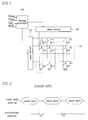
- FIG. 3 shows a schematic view of a data driver used for block addressing.
- the data driver includes a block select signal generator 100, an image signal processor 200, and switch blocks 300. All data lines are divided into an x-number of blocks, and each block has a y-number of data lines.
- the image signal processor 200 writes image data SIG to the selected block. That is, the image data SIG output from the image signal processor 200 are written on data lines of the LCD panel through the switch blocks 300 that are turned ON by the block select signal generator 100.
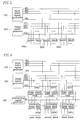
- FIG. 5 shows a detail view of an (n)th image signal select switch block 350n and an (n+1)th image signal select switch block 350n+1, and an (n)th precharging signal select switch block 360n and an (n+1)th precharging signal select switch block 360n+1 according to a first preferred embodiment of the present invention.
- the image signal select switch blocks 350n and 350n+1, and the precharging signal select switch blocks 360n and 360n+1 are comprised of a plurality of MOS transistors.
- sources of the MOS transistors are respectively connected to each of the image signals SIG1, SIG2,...,SIGy; gates of the MOS transistors are collectively connected to an (n)th block select signal BSn; and drains of the MOS transistors are respectively connected to each of the data lines of the LCD panel.
- sources of the MOS transistors of the (n+1)th precharging signal select switch block 360n+1 sources of the MOS transistors are collectively connected to the precharging signal PC; gates of the MOS transistors are collectively connected to the (n)th block select signal BSn; and drains of the MOS transistors are respectively connected to each of the data lines of the LCD panel.
- the transistors of both the (n)th image signal select switch block 350n and the (n+1)th precharging signal select switch block 360n+1 are turned ON. Accordingly, the image signals SIG1, SIG2,...SIGY are transmitted to the data lines connected to the drains of the transistors of the (n)th image signal select switch block 350n, and the precharging signal PC is transmitted to the data lines connected to the drains of the transistors of the (n+1)th precharging signal select switch block 360n+1.
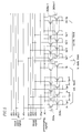
- the first precharging signal PC1 has a value between a maximum value Vmax and a center value Vcenter of the image signals SIG (hereinafter referred to as a "positive value”)
- the second precharging signal PC2 has a value between a minimum value Vmin and the center value Vcenter of the image signals SIG (hereinafter referred to as a "negative value").
- the values of the first and second precharging signals PC1 and PC2 change from a positive to a negative value in units of frames.
- the transistors of both the (n)th image signal select switch block 370n and the (n+1)th precharging signal select switch block 380n+1 are turned ON. Accordingly, the image signals SIG1, SIG2,...SIGY are transmitted to the data lines connected to the drains of the transistors of the (n)th image signal select switch block 370n, and the precharging signals PC1 and PC2 are transmitted to the data lines connected to the drains of the transistors of the (n+1)th precharging signal select switch block 380n+1.
- the first block of pixel lines may use a final block select signal of a previous pixel line to perform precharging/pre-discharging, or a separate first block precharging signal may be generated and used.
- the data lines are precharged a number of times (in each block interval), it is possible to reduce a required maximum current of the system when compared to the conventional method of precharging in the intervals between each horizontal line.
- a parasitic capacitance of each data line is 80pF
- a total load of 245.76nF (80pF x 3072) must be precharged.
- the data lines are divided into 16 blocks and each block is sequentially precharged, a significantly smaller 15.36nF load is used for precharging each block.
- the gate driver is not limited to the structure and operation described above, and can cover various modifications and equivalent arrangements.
- the AND gates of the gate array 540 shown in FIG. 11 can be replaced by NAND gates 551 of a gate array 550 as shown in FIG. 13.
- the NAND gates 551 and the inverters 552, 553 and 554 together act as AND gates.
- the use of the NAND gates 551 combined with the inverters 552, 553 and 554 improves a current drive capability of the gate signals supplied to the gate lines. This is due to the incremental size of the inverters 552, 553 and 554 connected to the NAND gates 551 such that the gate ON signals are able to be effectively transmitted to the gate lines.
Landscapes
- Engineering & Computer Science (AREA)
- Chemical & Material Sciences (AREA)
- Crystallography & Structural Chemistry (AREA)
- Physics & Mathematics (AREA)
- Computer Hardware Design (AREA)
- General Physics & Mathematics (AREA)
- Theoretical Computer Science (AREA)
- Control Of Indicators Other Than Cathode Ray Tubes (AREA)
- Liquid Crystal Display Device Control (AREA)
- Liquid Crystal (AREA)
Applications Claiming Priority (4)
| Application Number | Priority Date | Filing Date | Title |
|---|---|---|---|
| KR9836227 | 1998-09-03 | ||
| KR1019980036224A KR100296550B1 (ko) | 1998-09-03 | 1998-09-03 | 액정표시장치및그의구동방법및그의구동장치 |
| KR1019980036227A KR100274548B1 (ko) | 1998-09-03 | 1998-09-03 | 표시 장치 및 그의 방법 |
| KR9836224 | 1998-09-03 |
Publications (2)
| Publication Number | Publication Date |
|---|---|
| EP0984423A2 true EP0984423A2 (fr) | 2000-03-08 |
| EP0984423A3 EP0984423A3 (fr) | 2000-05-24 |
Family
ID=26634079
Family Applications (1)
| Application Number | Title | Priority Date | Filing Date |
|---|---|---|---|
| EP99116825A Withdrawn EP0984423A3 (fr) | 1998-09-03 | 1999-09-02 | Dispositif et procédé de commande d'affichage matriciel |
Country Status (5)
| Country | Link |
|---|---|
| US (2) | US6731266B1 (fr) |
| EP (1) | EP0984423A3 (fr) |
| JP (1) | JP4651761B2 (fr) |
| CN (1) | CN1146854C (fr) |
| TW (1) | TW530287B (fr) |
Cited By (7)
| Publication number | Priority date | Publication date | Assignee | Title |
|---|---|---|---|---|
| WO2002050809A3 (fr) * | 2000-12-18 | 2003-07-24 | Three Five Systems Inc | Pre-ecriture de trame dans un affichage a cristaux liquides |
| GB2427741A (en) * | 2005-06-27 | 2007-01-03 | Lg Philips Lcd Co Ltd | Method and apparatus for driving a liquid crystal display device capable of reducing the heating value of data driver |
| US7224333B2 (en) | 2002-01-18 | 2007-05-29 | Semiconductor Energy Laboratory Co. Ltd. | Display device and driving method thereof |
| US7274351B2 (en) | 2002-05-30 | 2007-09-25 | Sharp Kabushiki Kaisha | Driver circuit and shift register of display device and display device |
| EP1492077A4 (fr) * | 2002-03-29 | 2008-06-18 | Matsushita Electric Industrial Co Ltd | Dispositif d'affichage a cristaux liquides |
| US7663613B2 (en) | 2001-06-06 | 2010-02-16 | Semiconductor Energy Laboratory Co., Ltd. | Image display device and driving method thereof |
| CN103389848A (zh) * | 2013-08-08 | 2013-11-13 | 华映视讯(吴江)有限公司 | 驱动触控显示器的方法及提升信噪比的触控显示器 |
Families Citing this family (70)
| Publication number | Priority date | Publication date | Assignee | Title |
|---|---|---|---|---|
| GB9827988D0 (en) * | 1998-12-19 | 1999-02-10 | Koninkl Philips Electronics Nv | Active matrix liquid crystal display devices |
| US6892840B2 (en) * | 1999-05-05 | 2005-05-17 | Daniel J. Meaney, Jr. | Hybrid electric vehicle having alternate power sources |
| TW526464B (en) * | 2000-03-10 | 2003-04-01 | Sharp Kk | Data transfer method, image display device and signal line driving circuit, active-matrix substrate |
| KR100685942B1 (ko) * | 2000-08-30 | 2007-02-23 | 엘지.필립스 엘시디 주식회사 | 액정표시장치 및 그 구동방법 |
| KR100759972B1 (ko) * | 2001-02-15 | 2007-09-18 | 삼성전자주식회사 | 액정 표시 장치와 이의 구동 장치 및 방법 |
| KR100422593B1 (ko) * | 2001-05-03 | 2004-03-12 | 주식회사 하이닉스반도체 | 디코딩 장치 및 방법과 이를 사용한 저항열디지털/아날로그 컨버팅 장치 및 방법 |
| JP3744819B2 (ja) * | 2001-05-24 | 2006-02-15 | セイコーエプソン株式会社 | 信号駆動回路、表示装置、電気光学装置及び信号駆動方法 |
| JP3744818B2 (ja) | 2001-05-24 | 2006-02-15 | セイコーエプソン株式会社 | 信号駆動回路、表示装置、及び電気光学装置 |
| JP3744826B2 (ja) * | 2001-06-04 | 2006-02-15 | セイコーエプソン株式会社 | 表示制御回路、電気光学装置、表示装置及び表示制御方法 |
| JP3924754B2 (ja) * | 2001-06-06 | 2007-06-06 | 本田技研工業株式会社 | イメージセンサ |
| JP3606270B2 (ja) * | 2001-07-09 | 2005-01-05 | セイコーエプソン株式会社 | 電気光学装置の駆動方法、画像処理回路、電子機器、および補正データ生成方法 |
| KR100819138B1 (ko) * | 2001-08-25 | 2008-04-21 | 엘지.필립스 엘시디 주식회사 | 일렉트로 루미네센스 패널의 구동장치 및 그 구동방법 |
| JP3745259B2 (ja) * | 2001-09-13 | 2006-02-15 | 株式会社日立製作所 | 液晶表示装置およびその駆動方法 |
| US7106319B2 (en) * | 2001-09-14 | 2006-09-12 | Seiko Epson Corporation | Power supply circuit, voltage conversion circuit, semiconductor device, display device, display panel, and electronic equipment |
| JP3642042B2 (ja) * | 2001-10-17 | 2005-04-27 | ソニー株式会社 | 表示装置 |
| US20030085856A1 (en) * | 2001-11-02 | 2003-05-08 | Klein Terence R | System and method for minimizing image degradation in LCD microdisplays |
| JP3930332B2 (ja) | 2002-01-29 | 2007-06-13 | 富士通株式会社 | 集積回路、液晶表示装置、及び信号伝送システム |
| KR100438784B1 (ko) * | 2002-01-30 | 2004-07-05 | 삼성전자주식회사 | 박막 트랜지스터형 액정 표시 장치의 소스 드라이버의출력 회로 |
| KR100649243B1 (ko) * | 2002-03-21 | 2006-11-24 | 삼성에스디아이 주식회사 | 유기 전계발광 표시 장치 및 그 구동 방법 |
| US7126866B1 (en) * | 2002-08-10 | 2006-10-24 | National Semiconductor Corporation | Low power ROM architecture |
| KR100515299B1 (ko) * | 2003-04-30 | 2005-09-15 | 삼성에스디아이 주식회사 | 화상 표시 장치와 그 표시 패널 및 구동 방법 |
| JP3671973B2 (ja) * | 2003-07-18 | 2005-07-13 | セイコーエプソン株式会社 | 表示ドライバ、表示装置及び駆動方法 |
| KR100560468B1 (ko) * | 2003-09-16 | 2006-03-13 | 삼성에스디아이 주식회사 | 화상 표시 장치와 그 표시 패널 |
| KR100778409B1 (ko) * | 2003-10-29 | 2007-11-22 | 삼성에스디아이 주식회사 | 화상 표시 패널 및 그 구동 방법 |
| KR100515306B1 (ko) * | 2003-10-29 | 2005-09-15 | 삼성에스디아이 주식회사 | 유기el 표시패널 |
| KR100529077B1 (ko) * | 2003-11-13 | 2005-11-15 | 삼성에스디아이 주식회사 | 화상 표시 장치, 그 표시 패널 및 그 구동 방법 |
| KR100578911B1 (ko) * | 2003-11-26 | 2006-05-11 | 삼성에스디아이 주식회사 | 전류 역다중화 장치 및 이를 이용한 전류 기입형 표시 장치 |
| KR100578914B1 (ko) | 2003-11-27 | 2006-05-11 | 삼성에스디아이 주식회사 | 역다중화기를 이용한 표시 장치 |
| KR100578913B1 (ko) * | 2003-11-27 | 2006-05-11 | 삼성에스디아이 주식회사 | 역다중화기를 이용한 표시 장치 및 그 구동 방법 |
| KR100589381B1 (ko) * | 2003-11-27 | 2006-06-14 | 삼성에스디아이 주식회사 | 역다중화기를 이용한 표시 장치 및 그 구동 방법 |
| JP2005195810A (ja) * | 2004-01-06 | 2005-07-21 | Nec Electronics Corp | 容量性負荷駆動回路、及び表示パネル駆動回路 |
| TWI273540B (en) * | 2004-02-10 | 2007-02-11 | Sharp Kk | Display apparatus and driver circuit of display apparatus |
| JP2005227390A (ja) * | 2004-02-10 | 2005-08-25 | Sharp Corp | 表示装置のドライバ回路および表示装置 |
| JP4526415B2 (ja) * | 2004-03-15 | 2010-08-18 | シャープ株式会社 | 表示装置及び表示装置用ガラス基板 |
| KR101076424B1 (ko) * | 2004-03-31 | 2011-10-25 | 엘지디스플레이 주식회사 | 일렉트로 루미네센스 패널의 프리차지 방법 및 장치 |
| JP4285314B2 (ja) * | 2004-04-22 | 2009-06-24 | セイコーエプソン株式会社 | 電気光学装置 |
| KR100600350B1 (ko) * | 2004-05-15 | 2006-07-14 | 삼성에스디아이 주식회사 | 역다중화 및 이를 구비한 유기 전계발광 표시 장치 |
| KR100622217B1 (ko) * | 2004-05-25 | 2006-09-08 | 삼성에스디아이 주식회사 | 유기 전계발광 표시장치 및 역다중화부 |
| US20060012595A1 (en) * | 2004-07-19 | 2006-01-19 | Chien-Chih Chen | Driving circuit and driving process of display system |
| JP2006072078A (ja) * | 2004-09-03 | 2006-03-16 | Mitsubishi Electric Corp | 液晶表示装置及びその駆動方法 |
| KR101142995B1 (ko) * | 2004-12-13 | 2012-05-08 | 삼성전자주식회사 | 표시 장치 및 그 구동 방법 |
| KR101119729B1 (ko) * | 2004-12-31 | 2012-03-26 | 엘지디스플레이 주식회사 | 액정표시장치 |
| US7830352B2 (en) * | 2005-01-14 | 2010-11-09 | Au Optronics Corp. | Driving circuit for flat panel display which provides a horizontal start signal to first and second shift register cells |
| KR100685819B1 (ko) * | 2005-02-18 | 2007-02-22 | 삼성에스디아이 주식회사 | 초기화를 수행하는 필드순차 구동형 액정표시장치 |
| KR100685816B1 (ko) * | 2005-02-18 | 2007-02-22 | 삼성에스디아이 주식회사 | 필드순차 구동방법 및 필드순차 구동형 액정표시장치 |
| KR100685817B1 (ko) * | 2005-02-18 | 2007-02-22 | 삼성에스디아이 주식회사 | 필드순차방식 액정표시장치 |
| JP4624153B2 (ja) * | 2005-03-24 | 2011-02-02 | ルネサスエレクトロニクス株式会社 | 表示装置用駆動装置および表示装置用駆動方法 |
| TWI297484B (en) * | 2005-04-01 | 2008-06-01 | Au Optronics Corp | Time division driven display and method for driving same |
| JP2007017947A (ja) * | 2005-06-06 | 2007-01-25 | Seiko Epson Corp | 電気光学装置、駆動方法および電子機器 |
| JP5011788B2 (ja) * | 2005-06-17 | 2012-08-29 | セイコーエプソン株式会社 | 電気光学装置、駆動方法および電子機器 |
| KR20070005967A (ko) * | 2005-07-05 | 2007-01-11 | 삼성전자주식회사 | 액정표시장치와, 이의 구동 장치 및 방법 |
| KR101240645B1 (ko) * | 2005-08-29 | 2013-03-08 | 삼성디스플레이 주식회사 | 표시 장치 및 그 구동 방법 |
| US7830351B2 (en) * | 2005-10-11 | 2010-11-09 | Au Optronics Corporation | LCD gate driver circuitry having adjustable current driving capacity |
| JP2007148348A (ja) * | 2005-11-02 | 2007-06-14 | Seiko Epson Corp | 電気光学装置、その駆動方法および電子機器 |
| KR20070052051A (ko) | 2005-11-16 | 2007-05-21 | 삼성전자주식회사 | 액정 표시 장치의 구동 장치 및 이를 포함하는 액정 표시장치 |
| KR101263932B1 (ko) * | 2005-11-30 | 2013-05-15 | 삼성디스플레이 주식회사 | 액정 표시 패널의 데이터 구동 방법 및 장치 |
| TWI337451B (en) * | 2006-04-03 | 2011-02-11 | Novatek Microelectronics Corp | Method and related device of source driver with reduced power consumption |
| TW200739485A (en) * | 2006-04-07 | 2007-10-16 | Innolux Display Corp | Liquid crystal display, driving circuit and driving method thereof |
| JP2007279539A (ja) * | 2006-04-11 | 2007-10-25 | Nec Electronics Corp | ドライバ回路、表示装置及びその駆動方法 |
| JP2008170995A (ja) * | 2007-01-06 | 2008-07-24 | Samsung Electronics Co Ltd | 液晶表示装置及び液晶表示装置の残像除去方法 |
| TWI334126B (en) * | 2007-07-17 | 2010-12-01 | Au Optronics Corp | Voltage adjusting circuit, method, and display apparatus having the same |
| TWI396156B (zh) * | 2008-10-31 | 2013-05-11 | Au Optronics Corp | 資料線驅動方法 |
| TWI407187B (zh) * | 2009-07-14 | 2013-09-01 | Au Optronics Corp | 具感應機制之液晶顯示裝置與其感應定位方法 |
| TWI489430B (zh) | 2010-01-11 | 2015-06-21 | Novatek Microelectronics Corp | 顯示器的驅動裝置 |
| JP5206712B2 (ja) * | 2010-03-08 | 2013-06-12 | セイコーエプソン株式会社 | 画像表示装置及び電気光学装置の駆動方法並びに信号生成方法 |
| CN102005174B (zh) * | 2010-12-31 | 2013-06-05 | 福建华映显示科技有限公司 | 用于减少画面重影的方法 |
| KR102061595B1 (ko) * | 2013-05-28 | 2020-01-03 | 삼성디스플레이 주식회사 | 액정표시장치 및 그 구동방법 |
| TWI550590B (zh) * | 2015-05-22 | 2016-09-21 | 天鈺科技股份有限公司 | 資料驅動器、資料驅動器之驅動方法及顯示面板之驅動方法 |
| US11107442B2 (en) | 2018-05-24 | 2021-08-31 | Seiko Epson Corporation | Electro-optical device, driving method for electro-optical device, and electronic apparatus |
| TWI678577B (zh) * | 2018-11-23 | 2019-12-01 | 友達光電股份有限公司 | 應用於液晶顯示面板之資料處理方法 |
Family Cites Families (17)
| Publication number | Priority date | Publication date | Assignee | Title |
|---|---|---|---|---|
| JPS6180226A (ja) | 1984-09-28 | 1986-04-23 | Toshiba Corp | アクテイブ・マトリツクス駆動装置 |
| JPH0680477B2 (ja) | 1985-02-06 | 1994-10-12 | キヤノン株式会社 | 液晶表示パネル及び駆動方法 |
| JP2581796B2 (ja) * | 1988-04-25 | 1997-02-12 | 株式会社日立製作所 | 表示装置及び液晶表示装置 |
| JP2852390B2 (ja) * | 1991-02-16 | 1999-02-03 | 株式会社半導体エネルギー研究所 | 表示装置 |
| JP2806098B2 (ja) * | 1991-10-09 | 1998-09-30 | 松下電器産業株式会社 | 表示装置の駆動方法 |
| US5426447A (en) * | 1992-11-04 | 1995-06-20 | Yuen Foong Yu H.K. Co., Ltd. | Data driving circuit for LCD display |
| US5510807A (en) | 1993-01-05 | 1996-04-23 | Yuen Foong Yu H.K. Co., Ltd. | Data driver circuit and associated method for use with scanned LCD video display |
| JPH06337400A (ja) * | 1993-05-31 | 1994-12-06 | Sharp Corp | マトリクス型表示装置及び駆動方法 |
| JPH07152350A (ja) * | 1993-11-30 | 1995-06-16 | Sharp Corp | 表示装置及びその駆動方法 |
| JP3451717B2 (ja) * | 1994-04-22 | 2003-09-29 | ソニー株式会社 | アクティブマトリクス表示装置及びその駆動方法 |
| JP3482683B2 (ja) * | 1994-04-22 | 2003-12-22 | ソニー株式会社 | アクティブマトリクス表示装置及びその駆動方法 |
| JP3341530B2 (ja) * | 1995-04-11 | 2002-11-05 | ソニー株式会社 | アクティブマトリクス表示装置 |
| JP3110980B2 (ja) * | 1995-07-18 | 2000-11-20 | インターナショナル・ビジネス・マシーンズ・コーポレ−ション | 液晶表示装置の駆動装置及び方法 |
| JP3684699B2 (ja) * | 1996-02-09 | 2005-08-17 | セイコーエプソン株式会社 | D/a変換器、液晶パネル用基板及び液晶表示装置 |
| CN1166068C (zh) * | 1996-02-09 | 2004-09-08 | 精工爱普生株式会社 | D/a变换器及其设计方法、液晶屏用基片和液晶显示装置 |
| KR100214484B1 (ko) * | 1996-06-07 | 1999-08-02 | 구본준 | 순차 및 이중스캐닝방식을 위한 티에프티-엘씨디구동회로 |
| JP3666147B2 (ja) * | 1996-11-14 | 2005-06-29 | ソニー株式会社 | アクティブマトリクス表示装置 |
-
1999
- 1999-05-28 TW TW088108872A patent/TW530287B/zh not_active IP Right Cessation
- 1999-08-27 JP JP24146999A patent/JP4651761B2/ja not_active Expired - Fee Related
- 1999-09-02 EP EP99116825A patent/EP0984423A3/fr not_active Withdrawn
- 1999-09-03 CN CNB991184912A patent/CN1146854C/zh not_active Expired - Fee Related
- 1999-09-03 US US09/389,474 patent/US6731266B1/en not_active Expired - Fee Related
-
2001
- 2001-10-02 US US09/967,926 patent/US20020041267A1/en not_active Abandoned
Cited By (11)
| Publication number | Priority date | Publication date | Assignee | Title |
|---|---|---|---|---|
| WO2002050809A3 (fr) * | 2000-12-18 | 2003-07-24 | Three Five Systems Inc | Pre-ecriture de trame dans un affichage a cristaux liquides |
| US6850218B2 (en) | 2000-12-18 | 2005-02-01 | Brillian Corporation | Frame prewriting in a liquid crystal display |
| US7663613B2 (en) | 2001-06-06 | 2010-02-16 | Semiconductor Energy Laboratory Co., Ltd. | Image display device and driving method thereof |
| US8325170B2 (en) | 2001-06-06 | 2012-12-04 | Semiconductor Energy Laboratory Co., Ltd. | Image display device and driving method thereof |
| US7224333B2 (en) | 2002-01-18 | 2007-05-29 | Semiconductor Energy Laboratory Co. Ltd. | Display device and driving method thereof |
| EP1492077A4 (fr) * | 2002-03-29 | 2008-06-18 | Matsushita Electric Industrial Co Ltd | Dispositif d'affichage a cristaux liquides |
| US7274351B2 (en) | 2002-05-30 | 2007-09-25 | Sharp Kabushiki Kaisha | Driver circuit and shift register of display device and display device |
| GB2427741A (en) * | 2005-06-27 | 2007-01-03 | Lg Philips Lcd Co Ltd | Method and apparatus for driving a liquid crystal display device capable of reducing the heating value of data driver |
| GB2427741B (en) * | 2005-06-27 | 2007-08-29 | Lg Philips Lcd Co Ltd | Method and apparatus for driving liquid crystal display device |
| CN103389848A (zh) * | 2013-08-08 | 2013-11-13 | 华映视讯(吴江)有限公司 | 驱动触控显示器的方法及提升信噪比的触控显示器 |
| CN103389848B (zh) * | 2013-08-08 | 2016-07-06 | 华映视讯(吴江)有限公司 | 驱动触控显示器的方法及提升信噪比的触控显示器 |
Also Published As
| Publication number | Publication date |
|---|---|
| US20020041267A1 (en) | 2002-04-11 |
| US6731266B1 (en) | 2004-05-04 |
| CN1246698A (zh) | 2000-03-08 |
| JP4651761B2 (ja) | 2011-03-16 |
| CN1146854C (zh) | 2004-04-21 |
| TW530287B (en) | 2003-05-01 |
| EP0984423A3 (fr) | 2000-05-24 |
| JP2000089194A (ja) | 2000-03-31 |
Similar Documents
| Publication | Publication Date | Title |
|---|---|---|
| US6731266B1 (en) | Driving device and driving method for a display device | |
| US7508479B2 (en) | Liquid crystal display | |
| US10163392B2 (en) | Active matrix display device and method for driving same | |
| JP3451717B2 (ja) | アクティブマトリクス表示装置及びその駆動方法 | |
| JP3084293B2 (ja) | ピクセル反転動作を伴うlcdドライバic | |
| KR100361465B1 (ko) | 액정 패널 구동 방법 및 그 장치 | |
| TWI397734B (zh) | 液晶顯示器及其驅動方法 | |
| KR100683056B1 (ko) | 화상표시장치 | |
| US20030189537A1 (en) | Liquid crystal display and driving method thereof | |
| KR19980056458A (ko) | 박막트랜지스터 액정표시장치 | |
| KR100549983B1 (ko) | 액정표시장치 및 그 구동방법 | |
| US20040150599A1 (en) | Driver circuit, electro-optical device, and drive method | |
| GB2326013A (en) | Gate driver circuit for LCD | |
| KR101252854B1 (ko) | 액정 패널, 데이터 드라이버, 이를 구비한 액정표시장치 및그 구동 방법 | |
| KR101285054B1 (ko) | 액정표시장치 | |
| US20190318700A1 (en) | Display device and method for driving the same | |
| KR20010036308A (ko) | 이종 반전 구동법을 갖는 액정 표시 장치 및 이의 구동 방법 | |
| US8115716B2 (en) | Liquid crystal display device and its drive method | |
| KR100274548B1 (ko) | 표시 장치 및 그의 방법 | |
| KR100943631B1 (ko) | 액정 패널의 게이트 구동 장치 및 방법 | |
| KR20060067291A (ko) | 표시 장치 | |
| US6518947B1 (en) | LCD column driving apparatus and method | |
| KR101284940B1 (ko) | 액정표시소자의 구동 장치 및 방법 | |
| JP2005321510A (ja) | 表示装置及びその駆動制御方法 | |
| KR20030055892A (ko) | 2-도트 인버젼 구동방식의 액정표시장치 및 그 구동방법 |
Legal Events
| Date | Code | Title | Description |
|---|---|---|---|
| PUAI | Public reference made under article 153(3) epc to a published international application that has entered the european phase |
Free format text: ORIGINAL CODE: 0009012 |
|
| AK | Designated contracting states |
Kind code of ref document: A2 Designated state(s): DE FR GB NL |
|
| AX | Request for extension of the european patent |
Free format text: AL;LT;LV;MK;RO;SI |
|
| PUAL | Search report despatched |
Free format text: ORIGINAL CODE: 0009013 |
|
| RTI1 | Title (correction) |
Free format text: DEVICE AND METHOD FOR DRIVING MATRIX DISPLAY |
|
| AK | Designated contracting states |
Kind code of ref document: A3 Designated state(s): AT BE CH CY DE DK ES FI FR GB GR IE IT LI LU MC NL PT SE |
|
| AX | Request for extension of the european patent |
Free format text: AL;LT;LV;MK;RO;SI |
|
| 17P | Request for examination filed |
Effective date: 20001121 |
|
| AKX | Designation fees paid |
Free format text: DE FR GB NL |
|
| 17Q | First examination report despatched |
Effective date: 20070619 |
|
| STAA | Information on the status of an ep patent application or granted ep patent |
Free format text: STATUS: THE APPLICATION IS DEEMED TO BE WITHDRAWN |
|
| 18D | Application deemed to be withdrawn |
Effective date: 20120207 |