EP0984494B1 - Batterie de cellules solaires - Google Patents
Batterie de cellules solaires Download PDFInfo
- Publication number
- EP0984494B1 EP0984494B1 EP99902826A EP99902826A EP0984494B1 EP 0984494 B1 EP0984494 B1 EP 0984494B1 EP 99902826 A EP99902826 A EP 99902826A EP 99902826 A EP99902826 A EP 99902826A EP 0984494 B1 EP0984494 B1 EP 0984494B1
- Authority
- EP
- European Patent Office
- Prior art keywords
- solar cell
- layer
- cell
- cells
- electrode
- Prior art date
- Legal status (The legal status is an assumption and is not a legal conclusion. Google has not performed a legal analysis and makes no representation as to the accuracy of the status listed.)
- Expired - Lifetime
Links
- 239000000758 substrate Substances 0.000 claims description 25
- 238000009792 diffusion process Methods 0.000 claims description 22
- 239000012535 impurity Substances 0.000 claims description 17
- 239000001257 hydrogen Substances 0.000 claims description 11
- 229910052739 hydrogen Inorganic materials 0.000 claims description 11
- 229910052736 halogen Inorganic materials 0.000 claims description 10
- 150000002367 halogens Chemical class 0.000 claims description 10
- UFHFLCQGNIYNRP-UHFFFAOYSA-N Hydrogen Chemical compound [H][H] UFHFLCQGNIYNRP-UHFFFAOYSA-N 0.000 claims description 9
- 230000006798 recombination Effects 0.000 abstract description 27
- 238000005215 recombination Methods 0.000 abstract description 27
- 239000000969 carrier Substances 0.000 abstract description 25
- 239000002019 doping agent Substances 0.000 description 18
- 239000000463 material Substances 0.000 description 15
- 238000006243 chemical reaction Methods 0.000 description 14
- 230000007547 defect Effects 0.000 description 7
- 230000004888 barrier function Effects 0.000 description 6
- 238000010248 power generation Methods 0.000 description 6
- 229910001218 Gallium arsenide Inorganic materials 0.000 description 5
- 239000004065 semiconductor Substances 0.000 description 4
- 229910000980 Aluminium gallium arsenide Inorganic materials 0.000 description 3
- 230000015572 biosynthetic process Effects 0.000 description 3
- 230000000694 effects Effects 0.000 description 3
- 239000010408 film Substances 0.000 description 3
- IJGRMHOSHXDMSA-UHFFFAOYSA-N Atomic nitrogen Chemical compound N#N IJGRMHOSHXDMSA-UHFFFAOYSA-N 0.000 description 2
- VYPSYNLAJGMNEJ-UHFFFAOYSA-N Silicium dioxide Chemical compound O=[Si]=O VYPSYNLAJGMNEJ-UHFFFAOYSA-N 0.000 description 2
- 239000013078 crystal Substances 0.000 description 2
- 230000003247 decreasing effect Effects 0.000 description 2
- 238000010438 heat treatment Methods 0.000 description 2
- 150000002431 hydrogen Chemical class 0.000 description 2
- 230000003287 optical effect Effects 0.000 description 2
- 230000005855 radiation Effects 0.000 description 2
- 239000012780 transparent material Substances 0.000 description 2
- 229910000530 Gallium indium arsenide Inorganic materials 0.000 description 1
- 229910004205 SiNX Inorganic materials 0.000 description 1
- 238000010521 absorption reaction Methods 0.000 description 1
- QVGXLLKOCUKJST-UHFFFAOYSA-N atomic oxygen Chemical compound [O] QVGXLLKOCUKJST-UHFFFAOYSA-N 0.000 description 1
- 229910052681 coesite Inorganic materials 0.000 description 1
- 229910052906 cristobalite Inorganic materials 0.000 description 1
- 230000005284 excitation Effects 0.000 description 1
- 238000005468 ion implantation Methods 0.000 description 1
- 238000000034 method Methods 0.000 description 1
- 229910003465 moissanite Inorganic materials 0.000 description 1
- 229910052757 nitrogen Inorganic materials 0.000 description 1
- 239000001301 oxygen Substances 0.000 description 1
- 229910052760 oxygen Inorganic materials 0.000 description 1
- 229910010271 silicon carbide Inorganic materials 0.000 description 1
- 239000000377 silicon dioxide Substances 0.000 description 1
- 229910052682 stishovite Inorganic materials 0.000 description 1
- 239000010409 thin film Substances 0.000 description 1
- 229910052905 tridymite Inorganic materials 0.000 description 1
Images


Classifications
-
- H—ELECTRICITY
- H10—SEMICONDUCTOR DEVICES; ELECTRIC SOLID-STATE DEVICES NOT OTHERWISE PROVIDED FOR
- H10F—INORGANIC SEMICONDUCTOR DEVICES SENSITIVE TO INFRARED RADIATION, LIGHT, ELECTROMAGNETIC RADIATION OF SHORTER WAVELENGTH OR CORPUSCULAR RADIATION
- H10F19/00—Integrated devices, or assemblies of multiple devices, comprising at least one photovoltaic cell covered by group H10F10/00, e.g. photovoltaic modules
- H10F19/10—Integrated devices, or assemblies of multiple devices, comprising at least one photovoltaic cell covered by group H10F10/00, e.g. photovoltaic modules comprising photovoltaic cells in arrays in a single semiconductor substrate, the photovoltaic cells having vertical junctions or V-groove junctions
-
- H—ELECTRICITY
- H10—SEMICONDUCTOR DEVICES; ELECTRIC SOLID-STATE DEVICES NOT OTHERWISE PROVIDED FOR
- H10F—INORGANIC SEMICONDUCTOR DEVICES SENSITIVE TO INFRARED RADIATION, LIGHT, ELECTROMAGNETIC RADIATION OF SHORTER WAVELENGTH OR CORPUSCULAR RADIATION
- H10F10/00—Individual photovoltaic cells, e.g. solar cells
- H10F10/10—Individual photovoltaic cells, e.g. solar cells having potential barriers
- H10F10/14—Photovoltaic cells having only PN homojunction potential barriers
- H10F10/142—Photovoltaic cells having only PN homojunction potential barriers comprising multiple PN homojunctions, e.g. tandem cells
-
- H—ELECTRICITY
- H10—SEMICONDUCTOR DEVICES; ELECTRIC SOLID-STATE DEVICES NOT OTHERWISE PROVIDED FOR
- H10F—INORGANIC SEMICONDUCTOR DEVICES SENSITIVE TO INFRARED RADIATION, LIGHT, ELECTROMAGNETIC RADIATION OF SHORTER WAVELENGTH OR CORPUSCULAR RADIATION
- H10F10/00—Individual photovoltaic cells, e.g. solar cells
- H10F10/10—Individual photovoltaic cells, e.g. solar cells having potential barriers
- H10F10/14—Photovoltaic cells having only PN homojunction potential barriers
- H10F10/146—Back-junction photovoltaic cells, e.g. having interdigitated base-emitter regions on the back side
-
- H—ELECTRICITY
- H10—SEMICONDUCTOR DEVICES; ELECTRIC SOLID-STATE DEVICES NOT OTHERWISE PROVIDED FOR
- H10F—INORGANIC SEMICONDUCTOR DEVICES SENSITIVE TO INFRARED RADIATION, LIGHT, ELECTROMAGNETIC RADIATION OF SHORTER WAVELENGTH OR CORPUSCULAR RADIATION
- H10F19/00—Integrated devices, or assemblies of multiple devices, comprising at least one photovoltaic cell covered by group H10F10/00, e.g. photovoltaic modules
- H10F19/40—Integrated devices, or assemblies of multiple devices, comprising at least one photovoltaic cell covered by group H10F10/00, e.g. photovoltaic modules comprising photovoltaic cells in a mechanically stacked configuration
-
- Y—GENERAL TAGGING OF NEW TECHNOLOGICAL DEVELOPMENTS; GENERAL TAGGING OF CROSS-SECTIONAL TECHNOLOGIES SPANNING OVER SEVERAL SECTIONS OF THE IPC; TECHNICAL SUBJECTS COVERED BY FORMER USPC CROSS-REFERENCE ART COLLECTIONS [XRACs] AND DIGESTS
- Y02—TECHNOLOGIES OR APPLICATIONS FOR MITIGATION OR ADAPTATION AGAINST CLIMATE CHANGE
- Y02E—REDUCTION OF GREENHOUSE GAS [GHG] EMISSIONS, RELATED TO ENERGY GENERATION, TRANSMISSION OR DISTRIBUTION
- Y02E10/00—Energy generation through renewable energy sources
- Y02E10/50—Photovoltaic [PV] energy
- Y02E10/544—Solar cells from Group III-V materials
-
- Y—GENERAL TAGGING OF NEW TECHNOLOGICAL DEVELOPMENTS; GENERAL TAGGING OF CROSS-SECTIONAL TECHNOLOGIES SPANNING OVER SEVERAL SECTIONS OF THE IPC; TECHNICAL SUBJECTS COVERED BY FORMER USPC CROSS-REFERENCE ART COLLECTIONS [XRACs] AND DIGESTS
- Y02—TECHNOLOGIES OR APPLICATIONS FOR MITIGATION OR ADAPTATION AGAINST CLIMATE CHANGE
- Y02E—REDUCTION OF GREENHOUSE GAS [GHG] EMISSIONS, RELATED TO ENERGY GENERATION, TRANSMISSION OR DISTRIBUTION
- Y02E10/00—Energy generation through renewable energy sources
- Y02E10/50—Photovoltaic [PV] energy
- Y02E10/547—Monocrystalline silicon PV cells
Definitions
- the present invention relates to a solar cell, and more particularly to an improved tandem solar cell comprising stacked unit solar cells with different band gaps.
- Tandem solar cells comprising stacked unit solar cells with different band gaps are known as devices for providing improved photoelectric conversion efficiency by utilizing its wide wavelength range.
- An example of such a tandem solar cell is disclosed in Japanese Patent Laid-Open Publication No. Hei 4-226084 or in Japanese Patent Publication 59138386.
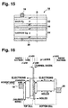
- Fig. 15 is a cross sectional view showing a conventional tandem solar cell.
- a solar cell 10 includes a top cell 12 which is a unit solar cell provided on the light incident side (top of the figure), a bottom cell 14 which is a unit solar cell provided on the back side, and a tunnel diode 16 provided between these cells.
- the solar cell also includes a top electrode 18 disposed on the light incident side, and a bottom electrode 20 on the back side.
- a solar cell with a wide band gap (Eg) is used for the top cell, while a solar cell with a narrow band gap is used for the bottom cell.
- Eg wide band gap
- Fig. 16 shows a band structure of the solar cell taken along the broken line D in Fig. 15.
- carriers i.e. electrons and holes
- the tunnel diode 16 is provided at the junction for permitting movement of carriers at this junction, so that the top cell 12 and the bottom cell 14 are connected in series to function as an integrated solar cell.
- the top and bottom cells 12 and 14 can absorb light with different wavelengths from each other, the above-described structure can absorb light with a wider range of wavelengths, to thereby enhance photoelectric conversion efficiency.
- the currents flowing through the top and bottom cells 12 and 14 must be equal to each other because the cells 12 and 14 are connected in series. Therefore, the top and bottom cells 12 and 14 of the solar cell 10 shown in Fig. 15 must have a thickness such that the same amount of carriers are generated in these cells and the same amount of currents flow therethrough. As a result, it is not possible to provide the cells with an optimum thickness for high photoelectric conversion efficiency.
- the solar cell suffers from a high defect density due to lattice mismatch at the interface between the top and bottom cells 12 and 14, leading to loss of minority carriers due to recombination at this portion.
- the present invention has been conceived in view of the above problems, and aims to provide a solar cell having a thickness most advantageous for a high photoelectric conversion efficiency and capable of reducing carrier recombination loss.
- the present invention provides a tandem solar cell as defined in claim 1.
- a multi-quantum well layer may be formed between the unit solar cells with different band gaps.
- the unit solar cell on the back side may include a diffusion layer having a higher impurity concentration than a substrate and provided at an uppermost surface thereof.
- the impurity concentration of the diffusion layer in the above solar cell may be set at 10-10 6 times that of the substrate.
- the unit solar cell on the back side may include an insulating layer provided at an uppermost surface thereof so as to form an opening at the surface.
- the total area of the opening may be preferably set to 0.01-10 % of the overall surface area.
- the total area of the opening may be also preferably set to 0.1-2 % of the overall surface area.
- the back electrodes provided at a back surface of the solar cell are individually connected to an n layer and a p layer formed on the back side to serve as the other electrode of the unit solar cell on the light incident side and as a pair of electrodes of the unit solar cell on the back side, wherein an intermediate layer containing hydrogen or halogen may be provided between the unit solar cells with different band gaps.
- the concentration of hydrogen or halogen is 1 ppm - 30 %.
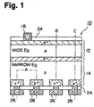
- Fig. 1 is a cross sectional view showing a structure of a solar cell according to the present invention.
- a solar cell 10 has a tandem structure including stacked top and bottom cells 12 and 14.
- the top cell 12 is a unit solar cell formed of a semiconductor material with a wide band gap (Eg)
- the bottom cell 14 is a unit solar cell formed of a semiconductor material with a narrow band gap.
- the top cell 12 is formed by stacking an n + layer, a p layer, and a p + layer, functioning as a unit solar cell on the light incident side.
- a top electrode 18 is provided connecting to the uppermost n + layer.
- An insulating layer 24 provided on top of the n + layer is formed of a transparent material, and through this layer 24, sunlight is incident on the solar cell 10.
- n + layers and p + layers are alternately provided at the back surface of the p layer serving as a substrate.
- a negative electrode 26 is individually connected to each n + layer, while a positive electrode 28 is individually connected to each p + layer, forming a back electrode of the present invention.
- the negative and positive electrodes 26 and 28 form a pair of electrodes of the bottom cell 14, and the positive electrode 28 is also used as an electrode forming a pair with the top electrode 18 which is one electrode of the top cell 12.
- the bottom cell 14 serves as a unit solar cell on the back side according to the present invention.
- the above-described top cell 12 can be formed of, for example, AlGaAs having a band gap of 1.82 eV.
- the n + layer has a dopant concentration of 1 x 10 19 cm -3 and a thickness of 0.1 ⁇ m
- the p layer has a dopant concentration of 1 x 10 16 cm -3 and a thickness of 1.0 ⁇ m
- the p + layer has a dopant concentration of 1 x 10 19 cm -3 and a thickness of 0.1 ⁇ m.
- the material suitable for the bottom cell 14 is Si having a band gap of 1.11 eV.
- the n + layer has a dopant concentration of 1 x 10 19 cm -3 and a thickness of 1.0 ⁇ m
- the p layer has a dopant concentration of 5 x 10 13 cm -3 and a thickness of 100 ⁇ m
- the p + layer has a dopant concentration of 1 x 10 19 cm -3 and a thickness of 1.0 ⁇ m.
- the top cell 12 can also be formed of InGaP or GaAs having a band gap of 1.88 eV and 1.42 eV, respectively.
- the bottom cell 14 can also be formed of GaAs with a band gap of 1.42 eV, or of Ge with a band gap of 0.66 eV.
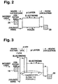
- Figs. 2-4 show band structures of the portions indicated by respective broken lines A, B, and C in Fig. 1. All these figures show the band structure at the time when the solar cell 10 is irradiated with light.
- the conduction band of the p + layer, the lowermost layer of the top cell 12 has the highest energy level.
- the electrons generated in the top cell 12 when the solar cell 10 is irradiated with incoming sunlight are transported toward the top electrode 18, while the electrons generated in the bottom cell 14 are transported toward the negative electrode 26 of the back electrode.
- the valence bands of the n + layers which are the uppermost and lowermost layers of the solar cell 10, have lower energy levels.
- holes cannot be transported along the portion B.
- the holes generated in the top and bottom cells 12 and 14 travel horizontally, when viewed as Fig. 1, in the respective cells, and then are transported along the portion C.
- the valence bands have the same energy levels in the portion indicated by the broken line C in Fig. 1. This is because the dopant concentrations of the p layer and p + layer in the top cell 12 and of the p layer in the bottom cell 14 are appropriately adjusted so that the energy levels of the valence bands of these layers will be equal upon receiving solar radiation.
- the n + layer is formed on the light reception side of the solar cell 10, while the p + layer is formed on the back side.
- Such a structure allows the holes generated in the top and bottom cells 12 and 14 to be transported toward the p+ layer on the back side and to be collected in the positive electrode 28, as shown in Fig. 4. Although the holes generated in the top cell 12 are transported through the interface between the top and bottom cells 12 and 14 in the course of the above-described transportation, no tunnel diodes are necessary because the energy levels are the same throughout the course of transportation.
- the conduction bands of the p layer and the p + layer of the top cell 12 and of the p + layer of the bottom cell 14 have higher energy levels, whereby the electrons generated in the p layer of the bottom cell 14 cannot be transported along the portion C shown in Fig. 1. Therefore, the electrons generated therein are transported horizontally, when viewed as Fig. 1, in the bottom cell 14, and then are transported along the portion B. On the other hand, the electrons generated in the p layer and the p + layer of the top cell 12 are transported toward the n + layer of the top cell 12 before being collected in the top cell 18.
- the negative and positive electrodes 26 and 28 provided at the back side of the bottom cell 14 function as a pair of electrodes of the bottom cell 14, and the positive electrode 28 is also used as the other electrode of the top cell 12, forming a pair with the top electrode 18 which is one electrode of the top cell 12.
- the above-described structure allows the electrons and holes generated in the bottom cell 14 to be collected in the negative electrode 26 and the positive electrode 28, respectively.
- the electrons generated in the top cell 12 are transported along the portion B to the n + layer of the top cell 12, and are collected in the top electrode 18.
- the holes generated in the top and bottom cells 12 and 14 travel along the portion C to the p + layer of the bottom cell 14, and are collected in the positive electrode 28.
- the solar cell 10 includes two stacked unit solar cells, i.e. the top cell 12 and the bottom cell 14.
- the two cells are not connected in series as in the conventional device, and therefore it is not necessary to match the amounts of currents in the top and bottom cells 12 and 14.
- the n + layers are provided at the top of the top cell 12 and the bottom of the bottom cell 14, the electrons generated in these cells are transpoted to the respective n + layers, and are collected in the top electrode 18 on the light incident side and the negative electrode 26 on the back side, respectively.
- the traveling distance of the minority carriers, i.e. electrons can be reduced, to thereby decrease recombination loss.
- the carriers need not pass through the energy barrier, and therefore no tunnel diodes are necessary.
- the need for forming tunnel diodes is eliminated, and carrier recombination loss and resistance loss in the tunnel diode can be avoided.
- an n type substrate can also be used. Although with an n type substrate the relations between the conduction band and the valence band and between electrons and holes will be contrary to those described above, a device with the same functions can be obtained.
- Fig. 5 is a cross sectional view showing a second embodiment of the solar cell according to the present invention.
- a multi-quantum well layer 22 formed by stacking two kinds of thin films with different band gaps is provided as the lowermost layer of the top cell 12.
- the multi-quantum well layer 22 is used as a means for utilizing optical excitation therein to improve photoelectric conversion efficiency in the solar cell. It should be noted that the layer 22 is formed between the top and bottom cells 12 and 14 in the present embodiment, while conventionally such a multi-quantum well layer has been formed between the p-n junction.
- This structure aims to eliminate any need for the carriers generated in the solar cell 10, especially the minority carriers, to pass through the multi-quantum well layer 22, to thereby prevent loss due to recombination of the minority carriers in the layer 22.
- the structure of the solar cell according to this embodiment is identical to that of the first embodiment shown in Fig. 1, except that the multi-quantum well layer 22 is provided between the top and bottom cells 12 and 14.
- An example of the material which has a wide band gap and can be used for the multi-quantum well layer 22 is AlGaAs having a band gap (Eg) of 1.82 eV.
- the dopant concentration is 1 x 10 16 cm -3 , and the thickness is 20 nm.
- GaAs can be used having a band gap of 1.42 eV. In this case, the dopant concentration is 1 x 10 16 cm -3 , and the thickness is 10 nm.
- GaAs with a band gap of 1.42 eV can also be used. With this material, the dopant concentration is 1 x 10 16 cm -3 , and the thickness is 30 nm. Also, InGaAs having a band gap of 1.25 eV can also be used as a material with a narrow band gap. In this case, the dopant concentration is 1 x 10 16 cm -3 , and the thickness is 15 nm.
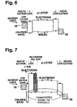
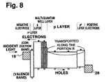
- Figs. 6-8 show band structures of the portions indicated by broken lines A, B, and C in Fig. 5, respectively. All these structures are related to those obtained when sunlight is incident on the solar cell 10.
- the band structure in Fig. 6 of the portion A shown in Fig. 5 is the same as that of the first embodiment shown in Fig. 2. Therefore, the electrons generated in the bottom cell 14 are transported to the n + layer, and are then collected in the positive electrode 26. Meanwhile, holes travel to the p + layer and are collected in the positive electrode 28.
- the conduction bands of the p layer and the multi-quantum well layer 22 of the top cell 12 have the highest energy levels at the portion indicated by the broken line B shown in Fig. 5. Consequently, the electrons generated in the p layer and the multi-quantum well layer 22 of the top cell 12 are transported to the n + layer of the top cell 12, and are then collected in the top electrode 18. The electrons generated in the bottom cell 14 are transported to the n + layer provided on the back side of the bottom cell 14 because the energy barrier at the multi-quantum well layer 22 is high, and are then collected in the negative electrode 26 of the back electrode.
- n + layers are formed at the surface on the light incident side and the back surface of the solar cell 10, and the electrons generated in the top and bottom cells 12 and 14 are transported to the n + layers on the light incident side and the back side, respectively.
- the minority carriers; i.e. electrons need not be transported through the multi-quantum well layer 22 which would otherwise cause a great carrier recombination loss.
- the traveling distance of electrons can also be reduced, to thereby improve power generation efficiency of the solar cell 10.
- the energy levels of the valence bands of the n + layers on the opposing sides of the solar cell 10 are lower, and those of the p layers and the multi-quantum well layer 22 provided therebetween are higher, as shown in Fig. 7. Consequently, the holes generated in the top and bottom cells 12 and 14 cannot be transported along the portion indicated by the broken line B in Fig. 5, but are transported horizontally, when viewed as Fig. 5, in the respective cells, and then along the portion C.
- the valence bands of the p layer and the multi-quantum well layer 22 in the top cell 12 and the p layer in the bottom cell 14 have the same energy level in the portion C indicated by the broken line in Fig. 5. As described earlier in conjunction with Fig. 4, this can be achieved by appropriately adjusting the dopant concentrations of the respective layers. As a result, the holes generated in the top cell 12, the multi-quantum well layer 22, and the bottom cell 14 travel to the p + layer formed on the back side of the bottom cell 14, and are then collected in the positive electrode 28.
- the holes generated in the top cell 12 pass through the multi-quantum well layer 22, this does not cause any problems because the multi-quantum well layer 22 of the present embodiment is formed of a p layer and recombination loss of the majority carriers (holes) is small.
- the conduction bands of the p layer and the multi-quantum well layer 22 of the top cell, and of the p + layer of the bottom cell 14 have higher energy levels. Therefore, the electrons generated in the bottom cell 14 cannot be transported toward the n + layer formed in the top cell 12. Thus, the electrons generated in the bottom cell 14 are transported horizontally, when viewed as Fig. 5, and along the portion B to the n + layer of the bottom cell 14, and are eventually collected in the negative electrode 26. The electrons generated in the top cell 12 travel toward the n + layer provided in the top cell 12, and are then collected in the top electrode 18.
- the minority carrier electrons generated in the top and bottom cells 12 and 14 need not pass through the multi-quantum well layer 22 which would otherwise cause a great recombination loss, thereby avoiding decrease in electrons due to recombination loss, and achieving improvement in power generation efficiency.
- the holes generated in the top cell 12 pass through the multi-quantum well layer 22 as described above, holes are the majority carriers in this embodiment and the energy level difference between the valence bands is small, and therefore recombination loss is suppressed to a small value.
- loss of carriers due to recombination is small and photoelectric conversion efficiency can be improved by effects of the multi-quantum well layer 22, whereby power generation efficiency of the solar cell 10 can further be enhanced according to the present embodiment.
- n-type substrate can also be used.
- the relations between the conduction band and the valence band and between electrons and holes are opposite to those described above, but solar cells with the same function can be implemented.
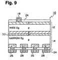
- Fig. 9 is a cross sectional view showing a third embodiment of the solar cell according to the present invention.
- a diffusion layer 30 having a higher impurity concentration than the substrate of the bottom cell 14 is provided at the uppermost surface of the bottom cell 14, that is, the interface between the top and bottom cells 12 and 14.
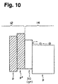
- Fig 10. illustrates a band structure of the portion surrounding the diffusion layer 30 shown in Fig. 9.
- providing the diffusion layer 30 with a high impurity concentration creates a potential difference between the diffusion layer 30 and the p layer serving as a substrate of the bottom cell 14, resulting in a barrier. Consequently, this barrier can prevent the minority carrier electrons generated in the bottom cell 14 from moving toward the interface between the top and bottom cells 12 and 14.
- recombination loss of the minority carriers (electrons) at the interface between the top and bottom cells 12 and 14 can be suppressed, leading to a further improvement in photoelectric conversion efficiency.
- the diffusion layer 30 has a higher impurity concentration than the substrate, there is a higher likelihood of carrier recombination in this layer. Therefore, the diffusion layer 30 preferably has a thickness of 5.0 ⁇ m or less, and more preferably, a thickness of 0.3-1.0 ⁇ m.
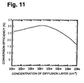
- Fig. 11 shows a relation between the impurity concentration of the above-described diffusion layer 30 and photoelectric conversion efficiency of the solar cell 10.
- the impurity concentration of the diffusion layer 30 is preferably 10-10 6 times, and more preferably 10 3 -10 4 times, as high as that of the p-type substrate of the bottom cell 14 described above. Carrier recombination in the diffusion layer 30 increases with the impurity concentration of the layer 30 exceeding 10 6 times that of the substrate.
- the impurity concentration of the diffusion layer 30 is less than 10 times the concentration of the substrate, the barrier shown in Fig. 10 becomes lower, and more minority carriers are transported beyond this barrier to reach the interface between the top and bottom cells 12 and 14.
- the impurity concentration of the diffusion layer 30 is in a range of 10-10 6 times as high as that of the substrate as described above.
- n-type substrate can alternatively be used.
- the relations between the conduction band and the valence band and between electrons and holes are opposite to the above-described relations, functionally the same solar cell can be implemented.
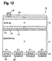
- Fig. 12 is a cross sectional view showing a structure of the solar cell according to a fourth embodiment of the present invention.
- the solar cell 10 has a tandem structure including the stacked top and bottom cells 12 and 14.
- the top cell 12 is a unit solar cell formed of a semiconductor material with a wide band gap (Eg)
- the bottom cell 14 is a unit solar cell formed of a semiconductor material with a narrow band gap.
- n + layer, a p layer, and a p + layer are stacked to form the top cell 12, serving as a unit solar cell on the light incident side according to the present invention.
- the top electrode 18 is disposed connected to the uppermost n + layer.
- the insulating film 24 formed of a transparent material is provided on top of the n + layer. Through this insulating film 24, sunlight is incident on the solar cell 10.
- n + layers and p + layers are alternatively formed at the back surface of the p layer functioning as a substrate.
- the negative electrode 26 is individually connected to each n + layer
- the positive electrode 28 is individually connected to each p + layer, forming a back electrode of the present invention.
- These negative and positive electrodes 26 and 28 form a pair of electrodes for the bottom cell 14, and the positive electrode 28 is also used as the electrode forming a pair with the top electrode 18 that is one electrode of the top cell 12.
- the bottom cell 14 corresponds to a unit solar cell on the back side according to the present invention.
- the above-described top cell 12 can be formed of, for example, AlGaAs, having a band gap of 1.82 eV. If this material is used, the n + layer has a dopant concentration of 1 x 10 19 cm -3 and a thickness of 0.1 ⁇ m, the p layer has a dopant concentration of 1 x 10 16 cm -3 and a thickness of 1.0 ⁇ m, and the p + layer has a dopant concentration of 1 x 10 19 cm -3 and a thickness of 0.1 ⁇ m.
- the material for the bottom cell 14 is Si, having a band gap of 1.11 eV.
- the n + layer has a dopant concentration of 1 x 10 19 cm -3 and a thickness of 1.0 ⁇ m
- the p layer has a dopant concentration of 5 x 10 13 cm -3 and a thickness of 100 ⁇ m
- the p + layer has a dopant concentration of 1 x 10 19 cm -3 and a thickness of 1.0 ⁇ m.
- GaAs with a band gap of 1.42 eV can be used to form the top cell 12
- Ge with a band gap of 0.66 eV can also be used to form the bottom cell 14.
- the present embodiment is characterized in that an insulating layer 32 is provided at the uppermost surface of the bottom cell 14.
- an unbonded valence electron present at the upper surface of the bottom cell 14 is bonded with oxygen or nitrogen forming the insulating layer 32, to thereby eliminate lattice defects. Consequently, recombination loss of the minority carriers caused by defects at the interface between the top and bottom cells 12 and 14 can be reduced.
- the insulating film 32 can be formed of materials such as SiO 2 , SiNx, and SiC, and preferably its thickness is in the range of 1-5000 nm, and more preferably in the range of 50-500 nm.
- an opening 34 is provided at a prescribed area ratio.
- the ratio of the area of the opening 34 to the overall surface area of the uppermost surface of the bottom cell 14 is 0.01-10%, and preferably 0.1-2%.
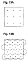
- Figs. 13A and 13B illustrate exemplary arrangement of the openings 34 provided in the insulating layer 32, in which the openings 34 are arranged in squares and hexagons, respectively. Arrangement patterns of the openings 34 other than these examples are also possible as long as they are substantially uniformly distributed at the upper surface of the bottom cell 14.
- Formation of the solar cell 10 begins with formation of the bottom cell 14, followed by provision of the insulating layer 32 on the uppermost surface thereof, and of the top cell 12.
- the p + layer of the top cell 12 formed on the insulating layer 32 has a larger grain size because the seed crystal portion thereof is limited to the opening 34, to thereby decrease crystal interface area and reduce carrier recombination loss at the interface.
- the impurity concentration of the p + layer in the opening 34 is further raised (to be a p ++ layer), movement of the carriers generated in the top cell 12 is facilitated, to thereby further reduce resistance loss.
- the solar cell 10 of the present embodiment makes it possible to decrease lattice defects at the uppermost surface of the bottom cell 14 by forming the insulating layer 32, reduce carrier recombination loss, and diminish resistance loss by providing the openings 34 in the insulating layer 32. As a result, a solar cell with a high power generation efficiency can be implemented.
- Fig. 14 is a cross sectional view showing a structure of the solar cell according to a fifth embodiment of the present invention.
- the elements identical to those in Fig. 12 are labeled with the same numerals in this figure, and will not be described again.
- the solar cell 10 includes an intermediate layer 36 containing hydrogen or halogen between the top and bottom cells 12 and 14.
- the intermediate layer 36 containing hydrogen or the like is formed on the uppermost surface of the bottom cell 14, followed by formation of the top cell 12 and heat treatment in reduction atmosphere, etc.
- elements such as hydrogen or halogen are diffused at the interface between the top and bottom cells 12 and 14, and bonded to unbonded valence electrons existing therein, to thereby reduce lattice defects at the interface, so that carrier recombination loss at the interface is decreased. Consequently, the amount of power generated in the tandem solar cell can be increased, and photoelectric conversion efficiency can be improved.
- the above intermediate layer 36 preferably has a thickness of, for example, 1-1000 nm. A greater thickness causes increase in resistance loss, and a smaller thickness weakens the effects given by the intermediate layer 36.
- the concentration of hydrogen, halogen, or the like contained in the intermediate layer 36 is preferably in the range of 1 ppm - 30 %. An excessively high concentration incurs a greater resistance loss, and the effects of the layer 36 cannot be fully exerted with an excessively low concentration thereof. Hydrogen or halogen can be added to the intermediate layer 36 by methods such as ion implantation.
- the intermediate layer 36 is formed at the uppermost surface of the bottom cell 14 in this embodiment, it can also be formed at the lowermost surface of the top cell 12.
- the insulating layer 32 having openings 34 of the fourth embodiment can also be provided to contain hydrogen, halogen, or the like, which is then diffused at the interface between the top and bottom cells 12 and 14 by heat treatment or the like, to thereby reduce unbonded valence electrons.
- the minority carriers generated in each of the unit solar cells with different band gaps are transported only within the unit solar cell where they are generated, so that a significant reduction in recombination loss can be achieved.
- the respective unit solar cells are not connected in series, and therefore carriers can be obtained for each unit solar cell, to thereby eliminate any need for matching the amounts of currents flowing through the respective unit solar cells.
- each of the unit solar cells can have an optimum thickness for the highest photoelectric conversion efficiency, so that power generation efficiency can be further enhanced.
- a further increase in photoelectric conversion efficiency can be obtained by forming a multi-quantum well layer between the respective unit solar cells.
- the diffusion layer formed at the uppermost surface of the bottom cell suppresses recombination of carriers at the interface between the top and bottom cells.
- the insulating layer contributes to reduction in lattice defects and the opening provided therein allows passage of carriers, whereby both recombination loss and resistance loss can be reduced simultaneously.
Landscapes
- Photovoltaic Devices (AREA)
Abstract
Claims (10)
- Cellule solaire en tandem (10) constituée par empilage d'une cellule solaire unitaire supérieure à large bande interdite et d'une cellule solaire inférieure à bande interdite étroite (12, 14) avec des bandes interdites différentes, comprenant :une électrode supérieure (18) placée sur la surface à lumière incidente de ladite cellule solaire en tandem et servant d'électrode de ladite cellule solaire unitaire supérieure du côté d'incidence de la lumière ; etdes première et deuxième électrodes postérieures (26, 28) placées sur une surface postérieure opposée à ladite surface à lumière incidente de ladite cellule solaire en tandem et connectée chacune à une couche n et à une couche p formées sur la surface postérieure de ladite cellule unitaire inférieure de manière à ce que les première et deuxième électrodes constituent une paire d'électrodes (26, 28) de ladite cellule solaire unitaire inférieure sur ledit côté postérieur et que l'une desdites première et deuxième électrodes de ladite paire serve d'autre électrode (28) de ladite cellule solaire unitaire supérieure sur le côté d'incidence de la lumière.
- Cellule solaire en tandem selon la revendication 1, dans laquelle une couche (22) de puits multi-quantiques est formée entre lesdites cellules solaires unitaires (12, 14) avec des bandes interdites différentes.
- Cellule solaire en tandem selon la revendication 1 dans laquelle, parmi lesdites cellules solaires unitaires avec des bandes interdites différentes, la cellule solaire unitaire inférieure (14) sur le côté postérieur comprend une couche de diffusion (30) ayant une concentration en impuretés plus élevée que celle d'un substrat et formée sur une surface la plus élevée de celui-ci.
- Cellule solaire selon la revendication 3, dans laquelle la concentration en impuretés de ladite couche de diffusion (30) est de 10 à 106 fois celle du substrat.
- Cellule solaire selon la revendication 4, dans laquelle la concentration en impuretés de ladite couche de diffusion (30) est de 103 à 104 fois celle du substrat.
- Cellule solaire en tandem selon la revendication 1 dans laquelle, parmi lesdites cellules solaires unitaires avec des bandes interdites différentes, la cellule solaire unitaire inférieure (14) sur le côté postérieur comprend une couche isolante (32) placée sur une surface la plus élevée de celle-ci de manière à constituer une ouverture (34) à ladite surface.
- Cellule solaire en tandem selon la revendication 6, dans laquelle la surface totale de ladite ouverture (34) est égale à 0,01 à 10 % de la surface globale.
- Cellule solaire en tandem selon la revendication 6, dans laquelle la surface totale de ladite ouverture (34) est égale à 0,1 à 2 % de la surface globale.
- Cellule solaire en tandem selon la revendication 1, dans laquelle une couche intermédiaire (36) contenant de l'hydrogène ou un halogène est placée entre les cellules solaires unitaires (12, 14) avec des bandes interdites différentes.
- Cellule solaire en tandem selon la revendication 9, dans laquelle la concentration dudit hydrogène ou halogène est de 1 partie par million à 30 %.
Applications Claiming Priority (7)
| Application Number | Priority Date | Filing Date | Title |
|---|---|---|---|
| JP07097698A JP3368822B2 (ja) | 1998-03-19 | 1998-03-19 | 太陽電池 |
| JP7097698 | 1998-03-19 | ||
| JP12477898A JP3368825B2 (ja) | 1998-05-07 | 1998-05-07 | 太陽電池 |
| JP12477898 | 1998-05-07 | ||
| JP36876798 | 1998-12-25 | ||
| JP36876798A JP3368854B2 (ja) | 1998-12-25 | 1998-12-25 | 太陽電池 |
| PCT/JP1999/000463 WO1999048157A1 (fr) | 1998-03-19 | 1999-02-04 | Batterie de cellules solaires |
Publications (3)
| Publication Number | Publication Date |
|---|---|
| EP0984494A1 EP0984494A1 (fr) | 2000-03-08 |
| EP0984494A4 EP0984494A4 (fr) | 2001-05-09 |
| EP0984494B1 true EP0984494B1 (fr) | 2004-09-29 |
Family
ID=27300498
Family Applications (1)
| Application Number | Title | Priority Date | Filing Date |
|---|---|---|---|
| EP99902826A Expired - Lifetime EP0984494B1 (fr) | 1998-03-19 | 1999-02-04 | Batterie de cellules solaires |
Country Status (6)
| Country | Link |
|---|---|
| EP (1) | EP0984494B1 (fr) |
| KR (1) | KR100326835B1 (fr) |
| CN (1) | CN1319179C (fr) |
| AU (1) | AU727351B2 (fr) |
| DE (1) | DE69920608T2 (fr) |
| WO (1) | WO1999048157A1 (fr) |
Families Citing this family (9)
| Publication number | Priority date | Publication date | Assignee | Title |
|---|---|---|---|---|
| US6166320A (en) * | 1998-03-19 | 2000-12-26 | Toyota Jidosha Kabushiki Kaisha | Tandem solar cell |
| JP4244549B2 (ja) | 2001-11-13 | 2009-03-25 | トヨタ自動車株式会社 | 光電変換素子及びその製造方法 |
| CN100477289C (zh) * | 2004-01-20 | 2009-04-08 | 瑟雷姆技术公司 | 具有外延生长量子点材料的太阳能电池 |
| US9018515B2 (en) | 2004-01-20 | 2015-04-28 | Cyrium Technologies Incorporated | Solar cell with epitaxially grown quantum dot material |
| KR100725110B1 (ko) * | 2005-12-14 | 2007-06-04 | 한국과학기술원 | 투과형 집적형 박막 태양전지 및 그 제조 방법. |
| EP2075850A3 (fr) * | 2007-12-28 | 2011-08-24 | Semiconductor Energy Laboratory Co, Ltd. | Dispositif de conversion photoélectrique et son procédé de fabrication |
| US8138410B2 (en) * | 2008-10-01 | 2012-03-20 | International Business Machines Corporation | Optical tandem photovoltaic cell panels |
| CN103094406B (zh) * | 2011-11-07 | 2015-11-04 | 太极能源科技股份有限公司 | 多晶硅太阳能电池及其制造方法 |
| CN103390622A (zh) * | 2012-05-11 | 2013-11-13 | 冠晶光电股份有限公司 | 层叠型太阳能电池结构 |
Family Cites Families (8)
| Publication number | Priority date | Publication date | Assignee | Title |
|---|---|---|---|---|
| JPS51113481A (en) * | 1975-03-28 | 1976-10-06 | Sony Corp | Semiconductor device |
| US4239554A (en) * | 1978-07-17 | 1980-12-16 | Shunpei Yamazaki | Semiconductor photoelectric conversion device |
| DE2834119C2 (de) * | 1978-08-03 | 1981-01-15 | Bayer Ag, 5090 Leverkusen | Verfahren zur Herstellung von Organopolysiloxanformmassen, die feinporige, gummielastische Formschaumkörper ergeben |
| JPS5923572A (ja) * | 1982-07-30 | 1984-02-07 | Matsushita Electric Works Ltd | 太陽電池 |
| JPS59138386A (ja) * | 1983-01-28 | 1984-08-08 | Nippon Telegr & Teleph Corp <Ntt> | 太陽電池 |
| JPS63222469A (ja) * | 1987-03-11 | 1988-09-16 | Mitsubishi Electric Corp | 積層型光起電力素子 |
| JPH03181180A (ja) * | 1989-12-11 | 1991-08-07 | Canon Inc | 太陽電池およびその製造方法 |
| JPH09213980A (ja) * | 1996-02-07 | 1997-08-15 | Toyota Motor Corp | 太陽電池の冷却方法 |
-
1999
- 1999-02-04 DE DE69920608T patent/DE69920608T2/de not_active Expired - Lifetime
- 1999-02-04 KR KR1019997010645A patent/KR100326835B1/ko not_active Expired - Fee Related
- 1999-02-04 EP EP99902826A patent/EP0984494B1/fr not_active Expired - Lifetime
- 1999-02-04 WO PCT/JP1999/000463 patent/WO1999048157A1/fr not_active Ceased
- 1999-02-04 AU AU22987/99A patent/AU727351B2/en not_active Ceased
- 1999-02-04 CN CNB998007617A patent/CN1319179C/zh not_active Expired - Fee Related
Also Published As
| Publication number | Publication date |
|---|---|
| DE69920608T2 (de) | 2005-10-06 |
| KR100326835B1 (ko) | 2002-03-04 |
| KR20010012684A (ko) | 2001-02-26 |
| CN1319179C (zh) | 2007-05-30 |
| DE69920608D1 (de) | 2004-11-04 |
| EP0984494A4 (fr) | 2001-05-09 |
| AU2298799A (en) | 1999-10-11 |
| WO1999048157A1 (fr) | 1999-09-23 |
| AU727351B2 (en) | 2000-12-14 |
| EP0984494A1 (fr) | 2000-03-08 |
| CN1272225A (zh) | 2000-11-01 |
Similar Documents
| Publication | Publication Date | Title |
|---|---|---|
| US6166320A (en) | Tandem solar cell | |
| TWI423454B (zh) | 具有晶格不匹配之GrIII-GrV-X層和組成分等之緩衝層的多接點太陽能電池 | |
| US8129614B2 (en) | Single P-N junction tandem photovoltaic device | |
| US20090173373A1 (en) | Group III-Nitride Solar Cell with Graded Compositions | |
| US8952242B2 (en) | Nanostructured quantum dots or dashes in photovoltaic devices and methods thereof | |
| KR102731634B1 (ko) | 태양전지 및 태양광 모듈 | |
| US20150162469A1 (en) | Dilute group iii-v nitride intermediate band solar cells with contact blocking layers | |
| US5215599A (en) | Advanced solar cell | |
| US20250324771A1 (en) | Multijunction solar cell structure | |
| CN115000213A (zh) | 光伏电池及其制造方法、光伏组件 | |
| EP0984494B1 (fr) | Batterie de cellules solaires | |
| JP3724272B2 (ja) | 太陽電池 | |
| JP3368822B2 (ja) | 太陽電池 | |
| JP3368854B2 (ja) | 太陽電池 | |
| JP2703167B2 (ja) | 受光素子及びその製造方法 | |
| KR102820593B1 (ko) | 직접형 반도체 광소자의 개선 | |
| KR20160082990A (ko) | 태양 전지 | |
| JP3368825B2 (ja) | 太陽電池 | |
| JPS6284570A (ja) | 光電池デバイス | |
| US20150090320A1 (en) | Solar cell | |
| JPS61288474A (ja) | 半導体装置 |
Legal Events
| Date | Code | Title | Description |
|---|---|---|---|
| PUAI | Public reference made under article 153(3) epc to a published international application that has entered the european phase |
Free format text: ORIGINAL CODE: 0009012 |
|
| 17P | Request for examination filed |
Effective date: 19991109 |
|
| AK | Designated contracting states |
Kind code of ref document: A1 Designated state(s): DE FR GB IT |
|
| A4 | Supplementary search report drawn up and despatched |
Effective date: 20010328 |
|
| AK | Designated contracting states |
Kind code of ref document: A4 Designated state(s): DE FR GB IT |
|
| RIC1 | Information provided on ipc code assigned before grant |
Free format text: 7H 01L 31/04 A, 7H 01L 31/068 B |
|
| 17Q | First examination report despatched |
Effective date: 20020613 |
|
| GRAP | Despatch of communication of intention to grant a patent |
Free format text: ORIGINAL CODE: EPIDOSNIGR1 |
|
| GRAS | Grant fee paid |
Free format text: ORIGINAL CODE: EPIDOSNIGR3 |
|
| GRAA | (expected) grant |
Free format text: ORIGINAL CODE: 0009210 |
|
| AK | Designated contracting states |
Kind code of ref document: B1 Designated state(s): DE FR GB IT |
|
| REG | Reference to a national code |
Ref country code: GB Ref legal event code: FG4D |
|
| REF | Corresponds to: |
Ref document number: 69920608 Country of ref document: DE Date of ref document: 20041104 Kind code of ref document: P |
|
| ET | Fr: translation filed | ||
| PLBE | No opposition filed within time limit |
Free format text: ORIGINAL CODE: 0009261 |
|
| STAA | Information on the status of an ep patent application or granted ep patent |
Free format text: STATUS: NO OPPOSITION FILED WITHIN TIME LIMIT |
|
| 26N | No opposition filed |
Effective date: 20050630 |
|
| PGFP | Annual fee paid to national office [announced via postgrant information from national office to epo] |
Ref country code: IT Payment date: 20060228 Year of fee payment: 8 |
|
| GBPC | Gb: european patent ceased through non-payment of renewal fee |
Effective date: 20070204 |
|
| PG25 | Lapsed in a contracting state [announced via postgrant information from national office to epo] |
Ref country code: GB Free format text: LAPSE BECAUSE OF NON-PAYMENT OF DUE FEES Effective date: 20070204 |
|
| PGFP | Annual fee paid to national office [announced via postgrant information from national office to epo] |
Ref country code: GB Payment date: 20060201 Year of fee payment: 8 |
|
| PG25 | Lapsed in a contracting state [announced via postgrant information from national office to epo] |
Ref country code: IT Free format text: LAPSE BECAUSE OF NON-PAYMENT OF DUE FEES Effective date: 20070204 |
|
| PGFP | Annual fee paid to national office [announced via postgrant information from national office to epo] |
Ref country code: FR Payment date: 20120221 Year of fee payment: 14 |
|
| PGFP | Annual fee paid to national office [announced via postgrant information from national office to epo] |
Ref country code: DE Payment date: 20120131 Year of fee payment: 14 |
|
| REG | Reference to a national code |
Ref country code: FR Ref legal event code: ST Effective date: 20131031 |
|
| REG | Reference to a national code |
Ref country code: DE Ref legal event code: R119 Ref document number: 69920608 Country of ref document: DE Effective date: 20130903 |
|
| PG25 | Lapsed in a contracting state [announced via postgrant information from national office to epo] |
Ref country code: FR Free format text: LAPSE BECAUSE OF NON-PAYMENT OF DUE FEES Effective date: 20130228 Ref country code: DE Free format text: LAPSE BECAUSE OF NON-PAYMENT OF DUE FEES Effective date: 20130903 |