EP0984520A2 - Kontrollierbarer elektrischer Verbinder für Gitterstiftsockel - Google Patents
Kontrollierbarer elektrischer Verbinder für Gitterstiftsockel Download PDFInfo
- Publication number
- EP0984520A2 EP0984520A2 EP99117230A EP99117230A EP0984520A2 EP 0984520 A2 EP0984520 A2 EP 0984520A2 EP 99117230 A EP99117230 A EP 99117230A EP 99117230 A EP99117230 A EP 99117230A EP 0984520 A2 EP0984520 A2 EP 0984520A2
- Authority
- EP
- European Patent Office
- Prior art keywords
- base
- electrical connector
- terminal
- generally
- cover
- Prior art date
- Legal status (The legal status is an assumption and is not a legal conclusion. Google has not performed a legal analysis and makes no representation as to the accuracy of the status listed.)
- Withdrawn
Links
- 230000037431 insertion Effects 0.000 claims abstract description 27
- 238000003780 insertion Methods 0.000 claims abstract description 27
- 229910000679 solder Inorganic materials 0.000 claims abstract description 19
- 238000005476 soldering Methods 0.000 claims description 8
- 229910052751 metal Inorganic materials 0.000 claims description 5
- 239000002184 metal Substances 0.000 claims description 5
- 238000011179 visual inspection Methods 0.000 claims description 4
- 230000000694 effects Effects 0.000 claims description 3
- 238000007689 inspection Methods 0.000 abstract description 4
- 230000014759 maintenance of location Effects 0.000 description 8
- XUIMIQQOPSSXEZ-UHFFFAOYSA-N Silicon Chemical compound [Si] XUIMIQQOPSSXEZ-UHFFFAOYSA-N 0.000 description 1
- 238000007792 addition Methods 0.000 description 1
- 229910052782 aluminium Inorganic materials 0.000 description 1
- XAGFODPZIPBFFR-UHFFFAOYSA-N aluminium Chemical compound [Al] XAGFODPZIPBFFR-UHFFFAOYSA-N 0.000 description 1
- 239000011248 coating agent Substances 0.000 description 1
- 238000000576 coating method Methods 0.000 description 1
- 239000000463 material Substances 0.000 description 1
- 238000004904 shortening Methods 0.000 description 1
- 229910052710 silicon Inorganic materials 0.000 description 1
- 239000010703 silicon Substances 0.000 description 1
- 229910001220 stainless steel Inorganic materials 0.000 description 1
- 239000010935 stainless steel Substances 0.000 description 1
- 239000003351 stiffener Substances 0.000 description 1
Images


Classifications
-
- H—ELECTRICITY
- H01—ELECTRIC ELEMENTS
- H01R—ELECTRICALLY-CONDUCTIVE CONNECTIONS; STRUCTURAL ASSOCIATIONS OF A PLURALITY OF MUTUALLY-INSULATED ELECTRICAL CONNECTING ELEMENTS; COUPLING DEVICES; CURRENT COLLECTORS
- H01R13/00—Details of coupling devices of the kinds covered by groups H01R12/70 or H01R24/00 - H01R33/00
- H01R13/46—Bases; Cases
- H01R13/502—Bases; Cases composed of different pieces
- H01R13/508—Bases; Cases composed of different pieces assembled by a separate clip or spring
-
- H—ELECTRICITY
- H01—ELECTRIC ELEMENTS
- H01R—ELECTRICALLY-CONDUCTIVE CONNECTIONS; STRUCTURAL ASSOCIATIONS OF A PLURALITY OF MUTUALLY-INSULATED ELECTRICAL CONNECTING ELEMENTS; COUPLING DEVICES; CURRENT COLLECTORS
- H01R13/00—Details of coupling devices of the kinds covered by groups H01R12/70 or H01R24/00 - H01R33/00
- H01R13/02—Contact members
- H01R13/22—Contacts for co-operating by abutting
- H01R13/24—Contacts for co-operating by abutting resilient; resiliently-mounted
-
- H—ELECTRICITY
- H01—ELECTRIC ELEMENTS
- H01R—ELECTRICALLY-CONDUCTIVE CONNECTIONS; STRUCTURAL ASSOCIATIONS OF A PLURALITY OF MUTUALLY-INSULATED ELECTRICAL CONNECTING ELEMENTS; COUPLING DEVICES; CURRENT COLLECTORS
- H01R12/00—Structural associations of a plurality of mutually-insulated electrical connecting elements, specially adapted for printed circuits, e.g. printed circuit boards [PCB], flat or ribbon cables, or like generally planar structures, e.g. terminal strips, terminal blocks; Coupling devices specially adapted for printed circuits, flat or ribbon cables, or like generally planar structures; Terminals specially adapted for contact with, or insertion into, printed circuits, flat or ribbon cables, or like generally planar structures
- H01R12/50—Fixed connections
- H01R12/51—Fixed connections for rigid printed circuits or like structures
- H01R12/52—Fixed connections for rigid printed circuits or like structures connecting to other rigid printed circuits or like structures
-
- H—ELECTRICITY
- H01—ELECTRIC ELEMENTS
- H01R—ELECTRICALLY-CONDUCTIVE CONNECTIONS; STRUCTURAL ASSOCIATIONS OF A PLURALITY OF MUTUALLY-INSULATED ELECTRICAL CONNECTING ELEMENTS; COUPLING DEVICES; CURRENT COLLECTORS
- H01R12/00—Structural associations of a plurality of mutually-insulated electrical connecting elements, specially adapted for printed circuits, e.g. printed circuit boards [PCB], flat or ribbon cables, or like generally planar structures, e.g. terminal strips, terminal blocks; Coupling devices specially adapted for printed circuits, flat or ribbon cables, or like generally planar structures; Terminals specially adapted for contact with, or insertion into, printed circuits, flat or ribbon cables, or like generally planar structures
- H01R12/70—Coupling devices
- H01R12/71—Coupling devices for rigid printing circuits or like structures
- H01R12/712—Coupling devices for rigid printing circuits or like structures co-operating with the surface of the printed circuit or with a coupling device exclusively provided on the surface of the printed circuit
- H01R12/714—Coupling devices for rigid printing circuits or like structures co-operating with the surface of the printed circuit or with a coupling device exclusively provided on the surface of the printed circuit with contacts abutting directly the printed circuit; Button contacts therefore provided on the printed circuit
-
- H—ELECTRICITY
- H01—ELECTRIC ELEMENTS
- H01R—ELECTRICALLY-CONDUCTIVE CONNECTIONS; STRUCTURAL ASSOCIATIONS OF A PLURALITY OF MUTUALLY-INSULATED ELECTRICAL CONNECTING ELEMENTS; COUPLING DEVICES; CURRENT COLLECTORS
- H01R12/00—Structural associations of a plurality of mutually-insulated electrical connecting elements, specially adapted for printed circuits, e.g. printed circuit boards [PCB], flat or ribbon cables, or like generally planar structures, e.g. terminal strips, terminal blocks; Coupling devices specially adapted for printed circuits, flat or ribbon cables, or like generally planar structures; Terminals specially adapted for contact with, or insertion into, printed circuits, flat or ribbon cables, or like generally planar structures
- H01R12/70—Coupling devices
- H01R12/82—Coupling devices connected with low or zero insertion force
- H01R12/85—Coupling devices connected with low or zero insertion force contact pressure producing means, contacts activated after insertion of printed circuits or like structures
- H01R12/89—Coupling devices connected with low or zero insertion force contact pressure producing means, contacts activated after insertion of printed circuits or like structures acting manually by moving connector housing parts linearly, e.g. slider
-
- Y—GENERAL TAGGING OF NEW TECHNOLOGICAL DEVELOPMENTS; GENERAL TAGGING OF CROSS-SECTIONAL TECHNOLOGIES SPANNING OVER SEVERAL SECTIONS OF THE IPC; TECHNICAL SUBJECTS COVERED BY FORMER USPC CROSS-REFERENCE ART COLLECTIONS [XRACs] AND DIGESTS
- Y10—TECHNICAL SUBJECTS COVERED BY FORMER USPC
- Y10S—TECHNICAL SUBJECTS COVERED BY FORMER USPC CROSS-REFERENCE ART COLLECTIONS [XRACs] AND DIGESTS
- Y10S439/00—Electrical connectors
- Y10S439/91—Observation aide, e.g. transparent material, window in housing
Definitions
- the present invention relates generally to an electrical connector and, more particularly, to an electrical connector for connecting a pin grid array (“PGA”) package, to a printed circuit board.
- PGA pin grid array
- a typical PGA includes a silicon chip, a package including conductive and non-conductive components and a plurality of pins depending downward from a bottom surface of the package.
- electrical connectors for PGA's include a base housing having an array of terminal receiving cavities, a plurality of terminals mounted in the terminal receiving cavities and a cover slidably mounted on the base housing.
- the cover has through holes therein adapted for insertion of the pins of the PGA therethrough. In operation, the cover is initially positioned in a first or pin receiving position. The pins of the PGA are then inserted through the holes in the cover.
- Some type of actuator is then typically actuated in order to slide the cover and the PGA with its associated pins linearly so that the pins engage the terminals contained within the base housing.
- An example of a connector of this type is disclosed in Japanese Patent Publication No. 2689325.
- the typical terminal of the connector of this type has a solder tail for soldering within a hole in a printed circuit board and of a contact piece for engaging a pin of the PGA.
- An engaging or retention portion is positioned between the solder tail and the contact piece for engaging the base housing in order to retain the terminal in the base housing.
- each terminal is formed into the configuration in which the contact piece, the engaging portion and the solder tail are linear as set forth above. Therefore, the terminal length is generally long, and the thickness of the base housing is generally similar to the length of the contact piece and the engaging portion. As a result, a reduction in the height of the overall electrical connector is generally difficult without also shrinking the height of the terminal.
- the present invention is intended to solve the problems set forth above. Therefore, it is an object of the present invention to provide an electrical connector for a PGA package having a structure adapted for inspection of the solder joints between the connector and the circuit member to which it is mounted.
- a zero insertion force electrical connector for mounting on a circuit member and receiving a device having an array of conductive pin terminals has a base housing having a generally planar lower surface and a plurality of terminal-receiving cavities corresponding to the array of pin terminals.
- a cover is slidably mounted on the base housing with the cover being movable between a first insertion position and a second engagement position.
- the cover also has a plurality of through holes therein arranged in an array corresponding to the array of pin terminals for receiving the pin terminals in the through holes.
- a plurality of stamped and formed conductive terminals are provided with one of the terminals being mounted in each of the cavities.
- Each terminal includes a generally planar base with the base being positioned generally adjacent the lower surface of the base housing and being oriented generally parallel to the plane of the lower surface.
- a mounting portion of the terminal is provided for securing the terminal in the base housing and a tail section is provided for contacting a conductive portion of the circuit member and includes a surface mount portion of the tail section positioned beneath the base.
- a contact structure is configured for engaging a portion of a respective one of the pin terminals the base includes a hole therein aligned with the surface mount portion of the tail section to permit visual inspection of the surface mount portion after the surface mount portion is solder to a surface of the circuit member.
- An actuating structure may be provided to slide the cover along the base housing between the first insertion position at which the pin terminals inserted into the through holes in the cover are spaced from the terminals and the second engagement position at which the pin terminals inserted into the through holes in the cover engage the contact structures of the terminals to effect electrical connection between the pin terminals and the circuit member.
- the base housing may be generally planar and made of plastic and the plane of the base housing oriented generally parallel to the plane of the lower surface of the base housing.
- the mounting portion of each terminal may extend generally perpendicularly to the base of the terminal.
- the mounting portion of each terminal may be positioned within a recess in the lower surface of the base housing.
- the tail section may extend from the base of the terminal.
- the tail section may also include a first arcuate section extending from the base and a second generally liner section extending from the first arcuate section generally away from the lower surface of the base housing at an oblique angle relative to the plane thereof to the surface mount portion.
- the contact structure may include a pair of spring arms extending generally perpendicularly from the base towards the cover. In some instances, the hole in the base may be round, and in other instances it may be oval.
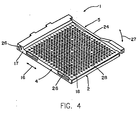
- Fig. 1 is an exploded view of a preferred embodiment of an electrical connector 1 for a PGA package. A slightly different embodiment is shown assembled in Fig. 4.
- an electrical connector 1 for receiving a PGA includes a base housing 2, a plurality of terminals 3 mounted in terminal receiving cavities 7 in the base housing 2, and a slidable cover 4 mounted on the upper side of the base housing..
- the base housing 2 is molded of dielectric plastic as a thin, generally rectangular plate.
- One end includes a mounting portion 6 for receiving an actuating lever 5 that drives the cover 4 back and forth in a linear fashion.
- Terminal receiving cavities 7 are formed in a grid array fashion over generally the entire area of the base housing 2 other than mounting portion 6 and as otherwise described below.
- the terminal receiving cavities 7 formed in grid array fashion are offset one half pitch in adjacent rows in both longitudinal and transverse directions as shown in Fig. 2. In other words, the cavities are located in a staggered fashion as a whole.
- each terminal 3 is stamped and formed of sheet metal, and includes a generally U-shaped spring contact 10 formed of a base piece 8 and a pair of contact arms 9 extending up from the base piece.
- a terminal retention piece 11 also extends upwardly from the base piece generally in parallel with the contact arms 9 for engaging a recess 14 in the lower surface 2a of base housing 2 in an interference fit in order to retain the terminal in the housing.
- the distal end of each contact arm 9 is inwardly bulged to form a contact portion 9a that engages a pin 15 of a PGA.
- a solder tail 12 extends from an edge of the base piece 8 opposite retention piece 11.
- the solder tail extends initially away from base piece 11 and then curves downward until it angles downward relative to the lower surface 2a of the base housing 6 in a generally linear manner to provide an appropriate tail for surface mount soldering on the surface of a printed circuit board 13. An end portion of the solder tail may extend upwards.
- An opening 8a (elliptical in Fig. 1 and round in Figs. 5 and 6) is provided in base piece 8 in order to permit inspection of the surface mount tail 12 from above once the base housing 2 and terminals 3 are soldered to printed circuit board 13 but before the cover 4 is mounted to the base housing.
- each terminal 3 is mounted from the bottom of base housing 2 through bottom surface 2a, and fixed in the base housing by an interference fit between the retention piece 11 and the recess 14.
- the cavities 7 are formed with a first insertion section or space 7a at which a pin 15 of a PGA may be inserted with zero insertion force and a second engagement section or space 7b which receives contact arms 9 of terminal 3.
- the cover 4 is formed in a generally rectangular plate configuration having a size generally similar to that of the base housing 2 as shown in the drawings.
- the cover 4 is formed of metal sheet (aluminum, stainless steel or the like).
- the cover 4 may be formed with the side edge portions 4a formed into a channel shaped configuration in cross section as shown in Fig. 1 or with the side edge portions 4b formed into an L-shaped configuration in cross section as shown in Fig. 4 for engaging with the side edge of the base housing 2.
- the side edge portions are adapted to guide the cover 4 as it slides in the direction of arrow 16 (Fig. 4) by operating the lever 5.
- the entire area of the cover 4 has through holes 18 provided in a grid array fashion corresponding to the terminal receiving cavities 7 of the base housing 2.
- the through holes 18 are adapted for insertion of the pins 15 of the PGA and, as best seen in Fig. 3, include counter bores or tapered sections 19 on the top surface of cover 4 and straight holes 20 extending from the counter bores 19 to the lower surface of the cover.
- the rear edge portion 17 of the cover 4 may be constructed with a stiffener 21 mounted with rivets 22 as shown in Fig. 1.
- the cover may be formed as a one-piece structure as shown in Fig. 4.
- the cover 4 formed of metal sheet is coated by an insulating coating or material such as an oxide film or the like to prevent it from electrically conducting with the pins 15 inserted into the through holes 18.
- an L-shaped actuating lever 5 includes crank bar or cam portion 23 and operating lever portion 24.
- the center section of the crank bar portion 23 is inserted into the mounting portion 6 of the base housing 2, and opposite end portions thereof are inserted into holes 25 formed in the engaging portions 17 of the cover 4.
- Snap rings 26 are mounted onto ends of crank bar portion 23 in order to secure the lever in the connector 1.
- a projection 30 extends from the bottom surface 2a of base housing 2 at a location aligned with each blank location 29 as shown in Figs. 2 and 3.
- a compliant pin 31 includes a press-fit retention section 32 that is secured within a recess in each projection 30 on the bottom surface 2a.
- Fig. 3 shows the preferred embodiment of the electrical connector 1 mounted on printed circuit board 13.
- Each compliant pin 31 projecting from the bottom surface 2a of the base housing 2 is engaged with an engaging hole 33 in the printed circuit board 13.
- the solder tails 12 of the terminals 3 that are arranged in a staggered fashion along the bottom surface 2a of the base housing 2 are positioned to be surface mount soldered to circuit pads (not shown) on the printed circuit board 13.
- Figs. 5 and 6 illustrate the position of the cover 4 relative to the base housing 2 and the terminals 3 in the insertion and engagement positions of the operating portion 24 of the lever 5.
- Fig. 5 is an illustration showing the condition in the insertion position of the operating portion 24. It can be seen that the through hole 18 in cover 4 is aligned with insertion section 7a so that pin 15 of the PGA may be inserted into through hole 18 without engaging contact arms 9 of terminal 3. This permits the insertion of the PGA into the connector 1 with essentially zero insertion force.
- the cover 4 By rotating operating lever 24 towards its engagement position, the cover 4 can be slidingly moved as indicated by arrow 16a to the position where the through hole 18 of the cover 4 is aligned with the spring contact 10 of the terminal 3.
- Fig. 6 shows this condition in which the operating portion 24 of lever 5 is in the engagement position.
- the through holes 18 in the cover 4 are aligned with the contact arms 9 of terminals 3.
- the pins located within the through holes 18 slide over ramps 9b of terminal 3 while deflecting the contact arms 9.
- the pins are positioned between and engage contact portions 9a of the terminal 3.
- the cover 4 slides as indicated by arrow 16b to move the through hole 18 with the pin 15 therein to the insertion section 7a of the terminal receiving cavity 7 in order to permit the PGA to be removed from the connector 1.
- the PGA When the PGA is connected to the printed circuit board 13 via the electrical connector 1, the PGA is placed on the cover 4 after the operating portion 24 of the lever 5 is in the insertion position, and the pins 15 are inserted into the insertion section 7a of the contact holes 7 via the through holes 18 of the cover 4.
- Each pin 15 is generally positioned between the spring contact 10 of each terminal 3 and the terminal retention piece 11.
- Each terminal 3 is configured whereby the spring contact 10 and engaging piece 11 are generally in parallel. Therefore, the contact arms 9 can achieve the desired spring characteristics by having an effective spring length generally similar to the thickness of the base housing 2. By removing the terminal retention section 11 from the electrical path and by providing redundant contact arms 9, improved electrical characteristics are provided.
- the length of the contact arms 9 and the thickness of the base housing 2 can be reduced as long as spring performance necessary for the desired electrical conduction can be provided. Therefore, reduction of the height of the electrical connector 1 can be achieved. Furthermore, by shortening the length of the contact arms 9 and by providing redundant parallel electrical paths, the inductance of the terminals 3 can be reduced which improves the connector's ability to transmit high speed signals. It should be noted that forming the cover 4 of metal sheet also contributes to a reduction of height or thickness of the electrical connector 1 since the cover 4 can provide the necessary strength even though it is extremely thin.
- the pins 15 of the PGA are moved away from engagement with the spring contacts 10 as indicated by arrow 16b in Fig. 6 to permit removal of the PGA from connector 1 without necessitating a large withdrawal force.
- the compliant pins 31 can protect the soldering portions of the solder tails 12.
- each terminal 3 has a generally U-shaped configuration with the bottom piece 8 and a pair of the contact arms 9, one arm could be removed so that the contact piece is not generally U-shaped but rather L-shaped.
- solder tail 12 of each terminal 3 is also not limited to the configuration adapted for surface mount soldering.
- the solder tails may be formed as pins that extend into through holes in the printed circuit board 13 and soldered by wave soldering.
Landscapes
- Connecting Device With Holders (AREA)
- Coupling Device And Connection With Printed Circuit (AREA)
Applications Claiming Priority (2)
| Application Number | Priority Date | Filing Date | Title |
|---|---|---|---|
| JP26727598 | 1998-09-04 | ||
| JP10267275A JP2000082555A (ja) | 1998-09-04 | 1998-09-04 | Pgaパッケージ用コネクタ |
Publications (2)
| Publication Number | Publication Date |
|---|---|
| EP0984520A2 true EP0984520A2 (de) | 2000-03-08 |
| EP0984520A3 EP0984520A3 (de) | 2001-06-13 |
Family
ID=17442582
Family Applications (3)
| Application Number | Title | Priority Date | Filing Date |
|---|---|---|---|
| EP99117162A Withdrawn EP0984518A3 (de) | 1998-09-04 | 1999-09-01 | Elekrischer Verbinder für Gitterstiftsockel |
| EP99117229A Withdrawn EP0984519A3 (de) | 1998-09-04 | 1999-09-02 | Elektrischer Verbinder mit niedriger Bauhöhe für Gitterstiftsockel und Anschlüsse dafür |
| EP99117230A Withdrawn EP0984520A3 (de) | 1998-09-04 | 1999-09-02 | Kontrollierbarer elektrischer Verbinder für Gitterstiftsockel |
Family Applications Before (2)
| Application Number | Title | Priority Date | Filing Date |
|---|---|---|---|
| EP99117162A Withdrawn EP0984518A3 (de) | 1998-09-04 | 1999-09-01 | Elekrischer Verbinder für Gitterstiftsockel |
| EP99117229A Withdrawn EP0984519A3 (de) | 1998-09-04 | 1999-09-02 | Elektrischer Verbinder mit niedriger Bauhöhe für Gitterstiftsockel und Anschlüsse dafür |
Country Status (8)
| Country | Link |
|---|---|
| US (2) | US6325655B1 (de) |
| EP (3) | EP0984518A3 (de) |
| JP (1) | JP2000082555A (de) |
| KR (3) | KR100344051B1 (de) |
| CN (3) | CN1139154C (de) |
| MY (1) | MY122395A (de) |
| SG (3) | SG87825A1 (de) |
| TW (3) | TW424985U (de) |
Families Citing this family (20)
| Publication number | Priority date | Publication date | Assignee | Title |
|---|---|---|---|---|
| JP3470314B2 (ja) * | 1999-07-05 | 2003-11-25 | 日本航空電子工業株式会社 | Zifコネクタ |
| US6386892B1 (en) * | 2001-11-21 | 2002-05-14 | Speed Tech Corp. | Tin paste overflow-protective electric connector |
| US6527577B1 (en) * | 2001-12-07 | 2003-03-04 | Hon Hai Precision Ind. Co., Ltd. | CPU socket having separate retention member |
| US6475012B1 (en) * | 2001-12-18 | 2002-11-05 | Hon Hai Precision Ind. Co., Ltd. | Device for CPU socket actuation |
| US6471536B1 (en) * | 2001-12-19 | 2002-10-29 | Hon Hai Precision Ind. Co., Ltd. | Zero Insertion Force socket having mechanical fastening device |
| TW525837U (en) * | 2002-03-08 | 2003-03-21 | Hon Hai Prec Ind Co Ltd | Electrical connector |
| US20040127085A1 (en) * | 2002-10-18 | 2004-07-01 | James Chen | Connector for a pin grid array integrated circuit device |
| US20040110050A1 (en) * | 2002-12-09 | 2004-06-10 | Abd Elhamid Mahmoud H | Environmentally friendly and inexpensive dielectric coolant for fuel cell stacks |
| US6857889B1 (en) * | 2003-09-26 | 2005-02-22 | General Motors Corporation | Vehicle body to chassis connection and method |
| JP4537732B2 (ja) * | 2004-03-04 | 2010-09-08 | 住友電装株式会社 | 基板用コネクタ |
| JP2005294163A (ja) * | 2004-04-02 | 2005-10-20 | Jst Mfg Co Ltd | 補強タブ付き電気コネクタ |
| CN2752992Y (zh) * | 2004-11-27 | 2006-01-18 | 番禺得意精密电子工业有限公司 | 电连接器 |
| US7056130B1 (en) * | 2005-02-09 | 2006-06-06 | Tyco Electronics Corporation | Socket connector with inspection datum windows |
| FR2898734B1 (fr) * | 2006-03-17 | 2011-11-18 | Abb Entrelec Sas | Connecteur formant un composant pour montage en surface |
| CN200959472Y (zh) * | 2006-09-15 | 2007-10-10 | 富士康(昆山)电脑接插件有限公司 | 电连接器 |
| US7371100B1 (en) * | 2007-02-06 | 2008-05-13 | Hon Hai Precision Ind. Co., Ltd. | Fastening structure for integrated circuit and electrical connector using same |
| US20090227124A1 (en) * | 2008-03-06 | 2009-09-10 | Cinch Connectors, Inc. | Electrical connector |
| US8367942B2 (en) * | 2009-10-27 | 2013-02-05 | Hon Hai Precision Ind. Co., Ltd. | Low profile electrical interposer of woven structure and method of making same |
| CN102723633A (zh) * | 2012-06-12 | 2012-10-10 | 上海市电力公司 | 一种用于插拔式电表的插头 |
| CN104485540A (zh) * | 2014-12-24 | 2015-04-01 | 常熟市斯佳登电器有限公司 | 拆卸式电源插头 |
Family Cites Families (23)
| Publication number | Priority date | Publication date | Assignee | Title |
|---|---|---|---|---|
| US4059323A (en) * | 1976-05-13 | 1977-11-22 | International Business Machines Corporation | Apparatus for interconnecting plural mating members |
| US4221446A (en) * | 1978-10-02 | 1980-09-09 | The Bendix Corporation | Electrical connector assembly |
| US4498725A (en) * | 1982-06-02 | 1985-02-12 | Amp Incorporated | Electrical connector |
| JPS59144893U (ja) * | 1983-03-17 | 1984-09-27 | 日本航空電子工業株式会社 | 軸直角移動コネクタ |
| US5092789A (en) * | 1990-08-15 | 1992-03-03 | Aries Electronics, Inc. | Electrical connector for ZIF PGA test socket |
| US5057031A (en) * | 1990-08-15 | 1991-10-15 | Aries Electronics, Inc. | Zero insertion force pin grid array test socket |
| JPH0555438A (ja) * | 1991-08-26 | 1993-03-05 | Rohm Co Ltd | 電子部品のリード端子構造 |
| US5256080A (en) * | 1992-06-12 | 1993-10-26 | The Whitaker Corporation | Bail actuated ZIF socket |
| US5456613A (en) * | 1993-07-16 | 1995-10-10 | Tongrand Limited | Zero insertion force connector and contact therein |
| JPH0730466U (ja) * | 1993-11-08 | 1995-06-06 | 住友電装株式会社 | コネクタ用雌端子金具 |
| US5454727A (en) * | 1994-02-10 | 1995-10-03 | Hsu; Fu-Yu | Electrical connector with ZIF socket |
| US5443591A (en) * | 1994-05-24 | 1995-08-22 | Tsai; Tien C. | Connector socket |
| US5588861A (en) * | 1994-07-15 | 1996-12-31 | Berg Technology, Inc. | ZIF chip socket |
| GB2295734A (en) * | 1994-10-11 | 1996-06-05 | Methode Electronics Inc | Zero insertion force socket |
| US5597320A (en) * | 1995-01-03 | 1997-01-28 | Molex Incorporated | Zero insertion force electrical connector and terminal |
| US5622514A (en) * | 1995-06-30 | 1997-04-22 | The Whitaker Corporation | Coverless pin grid array socket |
| US5535513A (en) * | 1995-08-25 | 1996-07-16 | The Whitaker Corporation | Method for making surface mountable connectors |
| US5679020A (en) * | 1995-09-29 | 1997-10-21 | Hon Hai Precision Ind. Co., Ltd. | Stopper for use with ZIF PGA socket |
| US5722848A (en) * | 1995-10-25 | 1998-03-03 | Hon Hai Precision Ind. Co., Ltd. | Retention mechanism for self-securement of ZIF PGA socket |
| US5692920A (en) * | 1995-12-14 | 1997-12-02 | Molex Incorporated | Zero insertion force electrical connector and terminal |
| US5697803A (en) * | 1996-06-20 | 1997-12-16 | The Whitaker Corporation | ZIF socket with hold open mechanism |
| JP3656175B2 (ja) * | 1996-10-09 | 2005-06-08 | 日本航空電子工業株式会社 | コネクタの駆動レバー取付構造 |
| US5762505A (en) * | 1996-12-02 | 1998-06-09 | Hon Hai Precision Ind. Co., Ltd. | Alignment device for use with a socket connector |
-
1998
- 1998-09-04 JP JP10267275A patent/JP2000082555A/ja active Pending
-
1999
- 1999-09-01 EP EP99117162A patent/EP0984518A3/de not_active Withdrawn
- 1999-09-01 SG SG9904243A patent/SG87825A1/en unknown
- 1999-09-01 SG SG9904245A patent/SG82018A1/en unknown
- 1999-09-01 SG SG9904242A patent/SG83149A1/en unknown
- 1999-09-02 US US09/388,846 patent/US6325655B1/en not_active Expired - Fee Related
- 1999-09-02 EP EP99117229A patent/EP0984519A3/de not_active Withdrawn
- 1999-09-02 EP EP99117230A patent/EP0984520A3/de not_active Withdrawn
- 1999-09-02 US US09/388,845 patent/US6287137B1/en not_active Expired - Fee Related
- 1999-09-03 CN CNB991218841A patent/CN1139154C/zh not_active Expired - Fee Related
- 1999-09-03 CN CN99122026A patent/CN1132268C/zh not_active Expired - Fee Related
- 1999-09-03 MY MYPI99003813A patent/MY122395A/en unknown
- 1999-09-03 CN CN99121875A patent/CN1132276C/zh not_active Expired - Fee Related
- 1999-09-04 KR KR1019990037514A patent/KR100344051B1/ko not_active Expired - Fee Related
- 1999-09-04 KR KR1019990037516A patent/KR100344048B1/ko not_active Expired - Fee Related
- 1999-09-04 KR KR1019990037515A patent/KR100344050B1/ko not_active Expired - Fee Related
- 1999-09-29 TW TW088215081U patent/TW424985U/zh unknown
- 1999-09-29 TW TW088215082U patent/TW427570U/zh not_active IP Right Cessation
- 1999-09-29 TW TW088215083U patent/TW421331U/zh not_active IP Right Cessation
Also Published As
| Publication number | Publication date |
|---|---|
| KR100344050B1 (ko) | 2002-07-19 |
| TW424985U (en) | 2001-03-01 |
| KR100344051B1 (ko) | 2002-07-22 |
| MY122395A (en) | 2006-04-29 |
| TW427570U (en) | 2001-03-21 |
| EP0984518A2 (de) | 2000-03-08 |
| KR20000022915A (ko) | 2000-04-25 |
| EP0984519A3 (de) | 2001-06-13 |
| KR100344048B1 (ko) | 2002-07-22 |
| JP2000082555A (ja) | 2000-03-21 |
| CN1139154C (zh) | 2004-02-18 |
| US6287137B1 (en) | 2001-09-11 |
| EP0984518A3 (de) | 2001-06-13 |
| SG83149A1 (en) | 2001-09-18 |
| EP0984519A2 (de) | 2000-03-08 |
| CN1247395A (zh) | 2000-03-15 |
| CN1132276C (zh) | 2003-12-24 |
| EP0984520A3 (de) | 2001-06-13 |
| SG87825A1 (en) | 2002-04-16 |
| CN1248806A (zh) | 2000-03-29 |
| KR20000022914A (ko) | 2000-04-25 |
| US6325655B1 (en) | 2001-12-04 |
| SG82018A1 (en) | 2001-07-24 |
| KR20000022916A (ko) | 2000-04-25 |
| CN1248807A (zh) | 2000-03-29 |
| CN1132268C (zh) | 2003-12-24 |
| TW421331U (en) | 2001-02-01 |
Similar Documents
| Publication | Publication Date | Title |
|---|---|---|
| US6287137B1 (en) | Inspectable electrical connector for a PGA package | |
| US7431591B2 (en) | Socket for electrical parts | |
| KR100351086B1 (ko) | 핀 격자 배열 패키지용 소켓 및 액추에이터 | |
| US5240430A (en) | Electrical connector for cable to circit board application | |
| EP1517601B1 (de) | Sockel für elektrische Teile | |
| US5489217A (en) | Zero insertion force pin grid array socket | |
| US6139348A (en) | Electric connector with an elastically deformable contact pin | |
| US7775821B2 (en) | Socket for burn-in tests | |
| US5692920A (en) | Zero insertion force electrical connector and terminal | |
| EP1049365B1 (de) | Steckdose für elektronische Bauteile | |
| US5791929A (en) | Zero insertion force electrical connector and terminal | |
| US6554634B1 (en) | Electrical contact for ZIF socket connector | |
| US6471535B1 (en) | Electrical socket | |
| KR200291690Y1 (ko) | 핀 격자 배열 패키지용 소켓 | |
| US6857888B2 (en) | Socket for electrical parts | |
| CA1107831A (en) | Electrical connector with spring ejector | |
| KR100394337B1 (ko) | 전기부품용 소켓 | |
| JPH11135217A (ja) | Icソケット | |
| JP3725456B2 (ja) | コンタクトピン及びicソケット | |
| US6902445B2 (en) | Socket for electrical parts | |
| US20020160643A1 (en) | IC socket and suction-chucking sheet used in the same | |
| US6181568B1 (en) | Electrical apparatus | |
| JP4079214B2 (ja) | 電気部品用ソケットの製造方法 | |
| JPH0673882U (ja) | プリント基板用コネクタ |
Legal Events
| Date | Code | Title | Description |
|---|---|---|---|
| PUAI | Public reference made under article 153(3) epc to a published international application that has entered the european phase |
Free format text: ORIGINAL CODE: 0009012 |
|
| AK | Designated contracting states |
Kind code of ref document: A2 Designated state(s): AT BE CH CY DE DK ES FI FR GB GR IE IT LI LU MC NL PT SE |
|
| AX | Request for extension of the european patent |
Free format text: AL;LT;LV;MK;RO;SI |
|
| PUAL | Search report despatched |
Free format text: ORIGINAL CODE: 0009013 |
|
| AK | Designated contracting states |
Kind code of ref document: A3 Designated state(s): AT BE CH CY DE DK ES FI FR GB GR IE IT LI LU MC NL PT SE |
|
| AX | Request for extension of the european patent |
Free format text: AL;LT;LV;MK;RO;SI |
|
| AKX | Designation fees paid | ||
| REG | Reference to a national code |
Ref country code: DE Ref legal event code: 8566 |
|
| STAA | Information on the status of an ep patent application or granted ep patent |
Free format text: STATUS: THE APPLICATION IS DEEMED TO BE WITHDRAWN |
|
| 18D | Application deemed to be withdrawn |
Effective date: 20011214 |