EP0984536A2 - Miroirs pour laser semi-conducteur - Google Patents
Miroirs pour laser semi-conducteur Download PDFInfo
- Publication number
- EP0984536A2 EP0984536A2 EP99307028A EP99307028A EP0984536A2 EP 0984536 A2 EP0984536 A2 EP 0984536A2 EP 99307028 A EP99307028 A EP 99307028A EP 99307028 A EP99307028 A EP 99307028A EP 0984536 A2 EP0984536 A2 EP 0984536A2
- Authority
- EP
- European Patent Office
- Prior art keywords
- layers
- layer
- refractive index
- temperature
- mirror
- Prior art date
- Legal status (The legal status is an assumption and is not a legal conclusion. Google has not performed a legal analysis and makes no representation as to the accuracy of the status listed.)
- Withdrawn
Links
Images


Classifications
-
- H—ELECTRICITY
- H01—ELECTRIC ELEMENTS
- H01S—DEVICES USING THE PROCESS OF LIGHT AMPLIFICATION BY STIMULATED EMISSION OF RADIATION [LASER] TO AMPLIFY OR GENERATE LIGHT; DEVICES USING STIMULATED EMISSION OF ELECTROMAGNETIC RADIATION IN WAVE RANGES OTHER THAN OPTICAL
- H01S5/00—Semiconductor lasers
- H01S5/02—Structural details or components not essential to laser action
- H01S5/028—Coatings ; Treatment of the laser facets, e.g. etching, passivation layers or reflecting layers
-
- H—ELECTRICITY
- H01—ELECTRIC ELEMENTS
- H01S—DEVICES USING THE PROCESS OF LIGHT AMPLIFICATION BY STIMULATED EMISSION OF RADIATION [LASER] TO AMPLIFY OR GENERATE LIGHT; DEVICES USING STIMULATED EMISSION OF ELECTROMAGNETIC RADIATION IN WAVE RANGES OTHER THAN OPTICAL
- H01S2304/00—Special growth methods for semiconductor lasers
- H01S2304/04—MOCVD or MOVPE
-
- H—ELECTRICITY
- H01—ELECTRIC ELEMENTS
- H01S—DEVICES USING THE PROCESS OF LIGHT AMPLIFICATION BY STIMULATED EMISSION OF RADIATION [LASER] TO AMPLIFY OR GENERATE LIGHT; DEVICES USING STIMULATED EMISSION OF ELECTROMAGNETIC RADIATION IN WAVE RANGES OTHER THAN OPTICAL
- H01S5/00—Semiconductor lasers
- H01S5/10—Construction or shape of the optical resonator, e.g. extended or external cavity, coupled cavities, bent-guide, varying width, thickness or composition of the active region
- H01S5/18—Surface-emitting [SE] lasers, e.g. having both horizontal and vertical cavities
- H01S5/183—Surface-emitting [SE] lasers, e.g. having both horizontal and vertical cavities having only vertical cavities, e.g. vertical cavity surface-emitting lasers [VCSEL]
- H01S5/18361—Structure of the reflectors, e.g. hybrid mirrors
-
- H—ELECTRICITY
- H01—ELECTRIC ELEMENTS
- H01S—DEVICES USING THE PROCESS OF LIGHT AMPLIFICATION BY STIMULATED EMISSION OF RADIATION [LASER] TO AMPLIFY OR GENERATE LIGHT; DEVICES USING STIMULATED EMISSION OF ELECTROMAGNETIC RADIATION IN WAVE RANGES OTHER THAN OPTICAL
- H01S5/00—Semiconductor lasers
- H01S5/30—Structure or shape of the active region; Materials used for the active region
- H01S5/32—Structure or shape of the active region; Materials used for the active region comprising PN junctions, e.g. hetero- or double- heterostructures
- H01S5/323—Structure or shape of the active region; Materials used for the active region comprising PN junctions, e.g. hetero- or double- heterostructures in AIIIBV compounds, e.g. AlGaAs-laser, InP-based laser
- H01S5/32308—Structure or shape of the active region; Materials used for the active region comprising PN junctions, e.g. hetero- or double- heterostructures in AIIIBV compounds, e.g. AlGaAs-laser, InP-based laser emitting light at a wavelength less than 900 nm
- H01S5/32341—Structure or shape of the active region; Materials used for the active region comprising PN junctions, e.g. hetero- or double- heterostructures in AIIIBV compounds, e.g. AlGaAs-laser, InP-based laser emitting light at a wavelength less than 900 nm blue laser based on GaN or GaP
Definitions
- the present invention relates to semiconductor lasers, and more particularly, to the fabrication of mirror elements in such lasers and to a method of manufacture thereof.
- Semiconductor lasers are widely used in optical disk drives and the like to write or read data. Since the density of data that can be stored on optical disks depends on the wavelength of the laser used to read and write the data, semiconductor lasers for generating light at short wavelengths are actively being pursued. Lasers based on Group III-V lasers emit light in the blue wavelengths; however, commercialization of this technology has been hampered by a number of problems.
- edge-emitting lasers There are two general types of semiconductor lasers, edge-emitting lasers and surface-emitting lasers.
- edge-emitting lasers the laser cavity is formed by utilizing cleaved facets to form the mirrors that define the edges of the cavity. Light exits the laser in a direction parallel to the substrate surface. While edge-emitting lasers are relatively easy to produce in single quantities, this technology cannot be easily utilized to form two-dimensional arrays of lasers.
- the cross-section of the laser generated light beam is rectangular, whereas circular beam cross-sections are preferred.
- surface-emitting lasers emit light in a direction perpendicular to the surface of the substrate.
- This type of laser lends itself to the construction of two-dimensional arrays.
- the cross-section of the laser beam can be controlled using conventional masking techniques, and hence, beams having circular cross-sections are easily obtained.
- the construction of surface-emitting lasers is much more complex than edge-emitting lasers.
- the mirrors are deposited as layers that are parallel to the substrate surface. While a number of technologies can be utilized to form the mirrors, semiconductor multi-layer film methods are preferred because the generation of the multilayer film utilizes the same equipment and process steps as the other layers in the laser structure.
- a multilayer film reflective mirror composed of GaN layers and InAlN layers is disclosed in Unexamined Japanese Patent Publication No. HEI 7-297476.
- Unexamined Japanese Patent Publication No. HEI 7-335975 discloses a multilayer reflective mirror composed of two types of AlGaN layers having different composition ratios of Al, Ga, and N.
- Group III-V nitride semiconductor surface-emitting lasers have advantages over edge-emitting lasers as discussed above, extending the lifetime, decreasing the threshold current, obtaining higher power output, and lowering manufacturing costs are needed. Significant progress toward these goals could be achieved if the number of layers in the mirrors could be reduced and the size and density of defects in the mirror layers could also be reduced.
- the number of layers required to fabricate a mirror of a given reflectivity depends on the ratio of the indices of refraction of the layers.
- the mirrors are formed by cyclically depositing layers of different indices of refraction.
- a repeated two-layer structure is utilized.
- the layers differ in index of refraction; hence, light will be partially reflected at the interface of the layers.
- the fraction of the light that is reflected at each interface depends on the ratio of the indices of refraction, greater ratios providing higher reflectivity.
- the thickness of the layers is chosen such that the light reflected from each boundary will add coherently. Hence, multilayer structures having the greatest difference in refractive index are preferred because fewer layers are needed.
- a GaN layer is grown at a high temperature on the substrate.
- a SiO 2 layer is in strips having widths of several microns on the surface of the GaN layer.
- GaN is grown over the SiO 2 strips by seeding further epitaxial growth from the GaN areas between the strips.
- the GaN that is formed over the SiO 2 in this manner is substantially defect-free except for a defect at the point at which the overgrowth from the two sides of the SiO 2 strip meets.
- this method does not lend itself to the formation of the mirror layers described above.
- a second method for reducing defects is referred to as the double buffer method.
- an amorphous GaN layer or AIN layer is grown to a thickness of several dozen nanometers on the substrate.
- a flat layer is then formed on top of this layer by growing a crystalline GaN layer having a thickness of several microns. This growing process is repeated twice to provide a GaN layer with reduced levels of defects.
- the double buffer technique is disclosed in the specification of Japanese Patent Application No. HEI 9-30215.
- the present invention is a mirror for use in a semiconductor laser.
- the mirror consists a total of four or more alternating layers of a low refractive index semiconductor material having an index of refraction of n 1 and a high refractive index semiconductor material having an index of refraction of n 2 where n 2 >n 1 .
- a first one of the layers is grown at a temperature, referred to as the "low temperature”, such that the layer is in a substantially amorphous state
- a second one of the layers is grown at a temperature, referred to as the "high temperature”, such that the layer is in a substantially monocrystalline state.
- the first one of the layers and the second one of the layers correspond to layers having different indices of refraction.
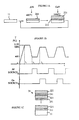
- Figures 1A-1C illustrate the fabrication of a mirror constructed from layers of GaN and AIN on a sapphire substrate.
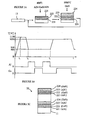
- FIGS 2A-2C illustrate an embodiment of the present invention in which the layers of the low refractive index material are formed by growth at the low temperature and the layers of high refractive index material are formed alternately by growth at the low temperature and growth at the high temperature.
- Figures 3A-3C illustrate the manner in which an upper mirror is formed using low temperature growth for forming both the low refractive index layers and the high refractive index layers.
- Figures 4A-4B illustrate the manner in which the present invention may be utilized to form a surface-emitting laser.
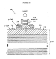
- Figures 5A-5J are cross-sectional views of a laser at various stages in the fabrication process.
- the layers that are grown to form the various mirror layers will be characterized by the temperature at which the layer is grown and by the relative index of refraction of the layers.
- the mirror layer having the lower index of refraction will be referred to as a "low refractive index layer”, and the layer having the higher index of refraction will be referred to as a "high refractive index layer”.
- the layers will be labeled by the temperatures with which the layers are grown.
- a "low temperature” layer refers to a layer that is grown at a temperature such that the resulting layer is substantially amorphous; while a “high temperature” layer refers to a layer that is grown at a temperature that produces a substantially monocrystalline material.
- the present invention is based on the observation that a relatively thick high temperature layer grown on top of a thin low temperature layer has acceptable defect densities even when the two materials have significantly different lattice constants.
- the thicknesses are constrained by the requirement that reflections from the various mirror layer interfaces must add coherently.
- the relative thicknesses of the layers are chosen to minimize the defects while providing a satisfactory crystalline state in the high temperature layer. As noted above, the thicknesses are also constrained by the need for coherent addition of the reflected light. This last constraint is satisfied if the layer thicknesses are chosen to be ⁇ /(4 ⁇ n) ⁇ ⁇ (2K - 1), where ⁇ is the wavelength of the light to be generated by the device, n is the index of refraction of the material in the layer, and K is a positive integer.
- the preferred Group III-V nitride materials for forming the low and high refractive index layers are AlN/GaN, AlGaN/GaN, InGaN/GaN or BGaN/GaN.
- a mirror according to the present invention is constructed by first forming a buffer layer utilizing low temperature growth on a substrate such as sapphire. Then the semiconductor layers are deposited on the buffer layer, the high refractive index layer being formed on the buffer layer and then the low refractive index layer being formed on the high refractive index layer.
- the buffer layer can be a single layer or multiple layers.
- the present invention may be practiced on a wide range of substrates in addition to the sapphire substrate discussed above.
- SiC, or MgAl 2 O 4 may be used as the substrate.
- a mirror according to the present invention does not need to be formed on the surface of the substrate or buffer layer.
- a mirror according to the present invention can be formed on the edge surface of the substrate.
- GaN has a refractive index of 2.67 and AIN has a refractive index of 2.20; hence, the GaN layer is the high refractive index layer and the AIN layer is the low refractive index layer.
- These materials have a lattice mis-match of about 2%. These materials also have a very large lattice mis-match with respect to the sapphire substrate.
- GaN has a lattice constant of 3.1 and sapphire has a lattice constant of 4.8.
- Figure 1A illustrates the deposition process used to generate the various mirror layers.
- Figure 1B illustrates the temperature changes of the nitrogen-containing (NH 3 ) atmosphere in the growth chamber during the deposition as a function of time, t.
- flow rates for the Ga source and the Al source are also plotted in Figure 1B.
- Figure 1C is a cross-sectional view of the resulting mirror.
- the surface of sapphire substrate 11 is first cleaned in the nitrogen atmosphere at approximately 1,150°C as shown at t 1 in Figure 1A and 1B.
- the temperature of the atmosphere is then lowered to approximately 400°C as shown at t 2 in Figure lB.
- the temperature of the atmosphere is raised from 400°C to approximately 1,000°C as shown at t 3 in Figure 1B.
- the GaN high refractive index layer 221 is then grown on the AlN low refractive index layer 211 to a thickness of 5 x 37.4 nm which corresponds to 5 ⁇ ⁇ /(4 ⁇ n AlN ).
- the process is then repeated.
- the next AIN low refractive index layer 211 is deposited at 400°C.
- the temperature is then raised to 1,000°C, and the next GaN high refractive index layer 221 is deposited.
- a mirror having 13 pairs of AIN/GaN layers has a reflectivity of 99.0% at a wavelength of 400 nm. If the number of pairs of layers is increased to 15, a reflectivity of 99.5% is obtained. When the number of pairs is increased to 19, a reflectivity of 99.9% is obtained.
- the first AIN layer formed by low temperature growth and the GaN layer formed thereon under high temperature growth conditions also function as a buffer layer for reducing threading dislocations caused by the lattice mismatch between sapphire and GaN.
- the low refractive index layers were formed growth at the low temperature, and the high refractive index layers were formed by growth at the high temperature.
- embodiments in which the low refractive index layers are formed by growth at the high temperature, and the high refractive index layers are formed by growth at the low temperature can also be practiced.
- Figure 2A-2C illustrate an embodiment of the present invention in which the layers of the low refractive index material are formed by low temperature growth and the layers of high refractive index material are formed alternatively by low temperature growth and by high temperature growth.
- Figure 2A is a diagrammatic view of the deposition process.
- Figure 2B is a graph of the temperature T of the atmosphere as a function of time, t, and the flow rates for the Ga and Al sources.
- Figure 2C is a cross-sectional view of the resultant mirror 32.
- the sapphire substrate 11 is first cleaned at a temperature of approximately 1,150°C as shown at time t 1 in Figure 2B. The temperature of the nitrogen atmosphere is then lowered to approximately 400°C as shown at t 2 .
- An AIN low refractive index layer 221 is then grown on the sapphire substrate 11 to a thickness of ⁇ /(4 ⁇ n AlN ).
- a GaN high refractive index layer 222 is grown on the AlN low refractive index layer 221 to a thickness of ⁇ /(4 ⁇ n GaN ).
- a second low temperature AIN low refractive index layer 223 is then grown on the GaN high refractive index layer 222 to a thickness of ⁇ /(4 ⁇ n AlN ).
- the temperature in the deposition chamber is increased to approximately 1,000°C as shown at time t 3 .
- a GaN high refractive index layer 224 is then grown on the AlN low refractive index layer 223 to a thickness of 5 ⁇ ⁇ /(4 x n GaN ).
- This four layer deposition process is then repeated until mirror 32 has 13 pairs of AlN/GaN layers as shown in Figure 2C.
- This embodiment of the present invention also provides a reflectivity of 99.0% reflectivity at a wavelength of 400 nm.
- the main advantage of this embodiment over that shown in Figure 1 is that the number of temperature cycles is half that of the embodiment shown in Figure 1, and hence, equilibration times are reduced and temperature control is simplified.
- Figure 3A is a cross-sectional view of a portion of an upper mirror during the deposition process.
- Figure 3B is a graph of the deposition temperature as a function of time, t. The states of the Ga and Al sources as a function of time are also shown in Figure 3B.
- Figure 3C is a cross-sectional view of mirror 33 after the various layers have been deposited.
- the mirror is being formed on a semiconductor layer 41 that is substantially free of dislocations.
- all of the mirror layers can be deposited at low temperature.
- the surface is cleaned in an atmosphere at a temperature of approximately 1,150°C.
- the temperature is then lowered to 400°C.
- An AIN low refractive index layer 231 is then grown to a thickness of ⁇ /(4 x n AlN ) on the semiconductor layer 41, and a GaN high refractive index layer 232 is grown to a thickness of ⁇ /(4 x n GaN ) on the AIN low refractive index layer 231.
- the process is repeated until 13 AlN/GaN pairs have been deposited as shown in Figure 3C.
- Mirror 33 has a reflectively of 99% at a wavelength of 400 nm.
- Figure 4A is a cross-sectional view of laser 5
- Figure 4B is a plot of the deposition temperature at various stages in the fabrication process.
- the layered structure which becomes the lower mirror 133 is deposited in the manner discussed with reference to the lower mirror embodiment shown in Figure 2A - 2C.
- the layered structure that is to become the active layer 134 is then deposited.
- the layered structure that becomes the upper mirror 135 is deposited in a manner analogous to that discussed above with respect to the upper mirror discussed in Figure 3A-3C.
- the n-AlGaN is grown to a thickness of ⁇ /(4 x n AlGaN ) (where n AlGaN is the refractive index of the AlGaN layer) at a temperature of 1,000°C on top of lower mirror 133.
- the last layer of mirror 133 is a GaN high refractive index layer that is also formed at a high temperature (1000°C).
- the temperature of the atmosphere in the deposition chamber is then lowered to 750°C, and an InGaN multiple quantum well (MQW) layer is formed on the n-AlGaN.
- MQW InGaN multiple quantum well
- the deposition temperature is then raised to 1,000°C, and the p-AlGaN is grown to a thickness of ⁇ /(4 x n AlGaN ). Then GaN is grown to a thickness of 5 ⁇ ⁇ /(4 x n GaN ) on the p-AlGaN layer.
- the final layer of lower mirror 133 is a GaN layer that is grown at high temperature to provide a single crystal on which active layer 134 is grown. This procedure reduces the lattice defects in active layer 134.
- FIGS. 5A-5J are cross-sectional views of a laser 100 at various stages in the fabrication process.
- a Ni patterned area is formed on the layered structure 5 as shown in Figure 5A.
- the top layers of the layered structure 5 are etched by reactive ion etching (RIE) until the p-GaN layer 136 shown in Figure 4A is reached to form the upper mirror 235 as shown in Figure 5B.
- RIE reactive ion etching
- a resist pattern 251 is formed to cover the entire upper mirror 235 as shown in Figure 5C.
- Ions are implanted into p-GaN layer 136 to increase the resistance of an area 252 around the upper mirror as shown in Figure 5D.
- the resist is then removed as shown in Figure 5E, and a Ni/Au/Ni layer 254 is deposited over the upper mirror and a portion ofthe implanted region as shown in Figure 5F.
- the areas of the layered structure 5 that are not protected by Ni/Au/Ni layer 254 are etched back to the n-GaN layer 138 in the bottom mirror 133 using RIE as shown in Figure 5G.
- the Ni/Au/Ni layers in the center of the upper mirror are etched to open the light-emitting aperture 255 as shown in Figure 5H.
- Al/Ti layers are deposited to provide the n-contacts 256 as shown in Figure 51.
- a more detailed cross-sectional view of the completed laser 100 is shown in Figure 5J.
Landscapes
- Physics & Mathematics (AREA)
- Condensed Matter Physics & Semiconductors (AREA)
- General Physics & Mathematics (AREA)
- Electromagnetism (AREA)
- Optics & Photonics (AREA)
- Semiconductor Lasers (AREA)
Applications Claiming Priority (2)
| Application Number | Priority Date | Filing Date | Title |
|---|---|---|---|
| JP25155698 | 1998-09-04 | ||
| JP10251556A JP2000091701A (ja) | 1998-09-04 | 1998-09-04 | 反射鏡、半導体レーザ、反射鏡の形成方法および半導体レーザの製造方法 |
Publications (2)
| Publication Number | Publication Date |
|---|---|
| EP0984536A2 true EP0984536A2 (fr) | 2000-03-08 |
| EP0984536A3 EP0984536A3 (fr) | 2000-05-17 |
Family
ID=17224586
Family Applications (1)
| Application Number | Title | Priority Date | Filing Date |
|---|---|---|---|
| EP99307028A Withdrawn EP0984536A3 (fr) | 1998-09-04 | 1999-09-03 | Miroirs pour laser semi-conducteur |
Country Status (3)
| Country | Link |
|---|---|
| US (1) | US6408015B1 (fr) |
| EP (1) | EP0984536A3 (fr) |
| JP (1) | JP2000091701A (fr) |
Families Citing this family (10)
| Publication number | Priority date | Publication date | Assignee | Title |
|---|---|---|---|---|
| DE10135806A1 (de) * | 2001-07-23 | 2003-02-13 | Zeiss Carl | Spiegel zur Reflexion elektromagnetischer Strahlung und Beleuchtungs- bzw. Abbildungsverfahren unter Einsatz desselben |
| JP3569807B2 (ja) * | 2002-01-21 | 2004-09-29 | 松下電器産業株式会社 | 窒化物半導体素子の製造方法 |
| US6967981B2 (en) * | 2002-05-30 | 2005-11-22 | Xerox Corporation | Nitride based semiconductor structures with highly reflective mirrors |
| KR100576870B1 (ko) | 2004-08-11 | 2006-05-10 | 삼성전기주식회사 | 질화물 반도체 발광소자 및 제조방법 |
| JP4300245B2 (ja) | 2006-08-25 | 2009-07-22 | キヤノン株式会社 | 多層膜反射鏡を備えた光学素子、面発光レーザ |
| JP4110181B2 (ja) * | 2006-09-01 | 2008-07-02 | キヤノン株式会社 | 半導体レーザ装置 |
| JP5747401B2 (ja) * | 2009-09-04 | 2015-07-15 | 住友化学株式会社 | 半導体基板、電界効果トランジスタ、集積回路、及び半導体基板の製造方法 |
| JP2012109499A (ja) * | 2010-11-19 | 2012-06-07 | Sony Corp | 半導体レーザ素子およびその製造方法 |
| JP6319975B2 (ja) * | 2013-09-11 | 2018-05-09 | 学校法人 名城大学 | 窒化物半導体混晶の製造方法 |
| JP6840352B2 (ja) | 2016-12-13 | 2021-03-10 | 学校法人 名城大学 | 半導体多層膜ミラー、これを用いた垂直共振器型発光素子及びこれらの製造方法 |
Family Cites Families (3)
| Publication number | Priority date | Publication date | Assignee | Title |
|---|---|---|---|---|
| US5146465A (en) | 1991-02-01 | 1992-09-08 | Apa Optics, Inc. | Aluminum gallium nitride laser |
| JPH0945987A (ja) | 1995-07-31 | 1997-02-14 | Hitachi Ltd | 半導体レーザ素子 |
| JP3082898B2 (ja) | 1995-10-18 | 2000-08-28 | 日本電信電話株式会社 | 反響消去装置 |
-
1998
- 1998-09-04 JP JP10251556A patent/JP2000091701A/ja active Pending
-
1999
- 1999-08-17 US US09/376,764 patent/US6408015B1/en not_active Expired - Fee Related
- 1999-09-03 EP EP99307028A patent/EP0984536A3/fr not_active Withdrawn
Also Published As
| Publication number | Publication date |
|---|---|
| EP0984536A3 (fr) | 2000-05-17 |
| US6408015B1 (en) | 2002-06-18 |
| JP2000091701A (ja) | 2000-03-31 |
Similar Documents
| Publication | Publication Date | Title |
|---|---|---|
| US6939730B2 (en) | Nitride semiconductor, semiconductor device, and method of manufacturing the same | |
| US6984841B2 (en) | Nitride semiconductor light emitting element and production thereof | |
| EP0949731B1 (fr) | Laser à semi-conducteur comprenant un composè de nitrure | |
| JP3571641B2 (ja) | 窒化物半導体素子 | |
| JP3910041B2 (ja) | 窒化物半導体レーザ素子及びこれを備えた半導体光学装置 | |
| US8368183B2 (en) | Nitride semiconductor device | |
| US7781796B2 (en) | Nitride semiconductor laser element | |
| JPH11135770A (ja) | 3−5族化合物半導体とその製造方法および半導体素子 | |
| US20010016404A1 (en) | GaN substrate including wide low - defect region for use in semiconductor element | |
| KR20010090499A (ko) | 질화물반도체소자 및 그 제조방법 | |
| US6408015B1 (en) | Mirror adapted for use in semiconductor lasers and method for fabricating the same | |
| US7709858B2 (en) | Nitride semiconductor light emitting device | |
| JP4854133B2 (ja) | 窒化物半導体レーザ素子とこれを含む光学装置 | |
| JP4625998B2 (ja) | 窒化物半導体レーザ素子 | |
| JPH09246651A (ja) | 窒化物半導体レーザ素子 | |
| US20080029770A1 (en) | Nitride semiconductor laser element | |
| JP4211358B2 (ja) | 窒化物半導体、窒化物半導体素子及びそれらの製造方法 | |
| EP0982819B1 (fr) | Formation par épitaxie des facettes des diodes laser en materiaux III-V | |
| JP5031674B2 (ja) | 窒化物半導体レーザ素子および窒化物半導体レーザ素子の製造方法 | |
| JP2003101157A (ja) | 半導体装置及びその製造方法 | |
| JP5532082B2 (ja) | 窒化物半導体レーザ素子 | |
| JP2007131527A (ja) | 窒化物半導体基板、窒化物半導体レーザ素子、窒化物半導体基板の製造方法、および窒化物半導体レーザ素子の製造方法 | |
| JP4415440B2 (ja) | 半導体レーザの製造方法 | |
| JP2004007009A (ja) | 窒化物半導体素子の製造方法 | |
| JP2006093548A (ja) | 窒化物半導体発光素子、及びその製造方法 |
Legal Events
| Date | Code | Title | Description |
|---|---|---|---|
| PUAI | Public reference made under article 153(3) epc to a published international application that has entered the european phase |
Free format text: ORIGINAL CODE: 0009012 |
|
| AK | Designated contracting states |
Kind code of ref document: A2 Designated state(s): DE FR GB |
|
| AX | Request for extension of the european patent |
Free format text: AL;LT;LV;MK;RO;SI |
|
| PUAL | Search report despatched |
Free format text: ORIGINAL CODE: 0009013 |
|
| AK | Designated contracting states |
Kind code of ref document: A3 Designated state(s): AT BE CH CY DE DK ES FI FR GB GR IE IT LI LU MC NL PT SE |
|
| AX | Request for extension of the european patent |
Free format text: AL;LT;LV;MK;RO;SI |
|
| 17P | Request for examination filed |
Effective date: 20001117 |
|
| AKX | Designation fees paid |
Free format text: DE FR GB |
|
| RAP1 | Party data changed (applicant data changed or rights of an application transferred) |
Owner name: HEWLETT-PACKARD COMPANY, A DELAWARE CORPORATION |
|
| RAP1 | Party data changed (applicant data changed or rights of an application transferred) |
Owner name: AGILENT TECHNOLOGIES INC. |
|
| RAP1 | Party data changed (applicant data changed or rights of an application transferred) |
Owner name: AGILENT TECHNOLOGIES INC. A DELAWARE CORPORATION |
|
| STAA | Information on the status of an ep patent application or granted ep patent |
Free format text: STATUS: THE APPLICATION HAS BEEN WITHDRAWN |
|
| RAP1 | Party data changed (applicant data changed or rights of an application transferred) |
Owner name: AGILENT TECHNOLOGIES, INC. (A DELAWARE CORPORATION |
|
| 18W | Application withdrawn |
Withdrawal date: 20010912 |