EP0985943A2 - Verfahren zur Herstellung eines faseroptischen Arrays und Vorrichtung zur Herstellung eines faseroptischen Arrays - Google Patents
Verfahren zur Herstellung eines faseroptischen Arrays und Vorrichtung zur Herstellung eines faseroptischen Arrays Download PDFInfo
- Publication number
- EP0985943A2 EP0985943A2 EP99117707A EP99117707A EP0985943A2 EP 0985943 A2 EP0985943 A2 EP 0985943A2 EP 99117707 A EP99117707 A EP 99117707A EP 99117707 A EP99117707 A EP 99117707A EP 0985943 A2 EP0985943 A2 EP 0985943A2
- Authority
- EP
- European Patent Office
- Prior art keywords
- bare fibers
- fibers
- fiber ribbons
- groove substrate
- bare
- Prior art date
- Legal status (The legal status is an assumption and is not a legal conclusion. Google has not performed a legal analysis and makes no representation as to the accuracy of the status listed.)
- Granted
Links
Images




Classifications
-
- G—PHYSICS
- G02—OPTICS
- G02B—OPTICAL ELEMENTS, SYSTEMS OR APPARATUS
- G02B6/00—Light guides; Structural details of arrangements comprising light guides and other optical elements, e.g. couplings
- G02B6/24—Coupling light guides
- G02B6/36—Mechanical coupling means
- G02B6/3628—Mechanical coupling means for mounting fibres to supporting carriers
- G02B6/3632—Mechanical coupling means for mounting fibres to supporting carriers characterised by the cross-sectional shape of the mechanical coupling means
- G02B6/3636—Mechanical coupling means for mounting fibres to supporting carriers characterised by the cross-sectional shape of the mechanical coupling means the mechanical coupling means being grooves
-
- G—PHYSICS
- G02—OPTICS
- G02B—OPTICAL ELEMENTS, SYSTEMS OR APPARATUS
- G02B6/00—Light guides; Structural details of arrangements comprising light guides and other optical elements, e.g. couplings
- G02B6/24—Coupling light guides
-
- G—PHYSICS
- G02—OPTICS
- G02B—OPTICAL ELEMENTS, SYSTEMS OR APPARATUS
- G02B6/00—Light guides; Structural details of arrangements comprising light guides and other optical elements, e.g. couplings
- G02B6/24—Coupling light guides
- G02B6/36—Mechanical coupling means
- G02B6/3628—Mechanical coupling means for mounting fibres to supporting carriers
- G02B6/368—Mechanical coupling means for mounting fibres to supporting carriers with pitch conversion between input and output plane, e.g. for increasing packing density
-
- G—PHYSICS
- G02—OPTICS
- G02B—OPTICAL ELEMENTS, SYSTEMS OR APPARATUS
- G02B6/00—Light guides; Structural details of arrangements comprising light guides and other optical elements, e.g. couplings
- G02B6/24—Coupling light guides
- G02B6/36—Mechanical coupling means
- G02B6/3628—Mechanical coupling means for mounting fibres to supporting carriers
- G02B6/3648—Supporting carriers of a microbench type, i.e. with micromachined additional mechanical structures
- G02B6/3652—Supporting carriers of a microbench type, i.e. with micromachined additional mechanical structures the additional structures being prepositioning mounting areas, allowing only movement in one dimension, e.g. grooves, trenches or vias in the microbench surface, i.e. self aligning supporting carriers
-
- G—PHYSICS
- G02—OPTICS
- G02B—OPTICAL ELEMENTS, SYSTEMS OR APPARATUS
- G02B6/00—Light guides; Structural details of arrangements comprising light guides and other optical elements, e.g. couplings
- G02B6/24—Coupling light guides
- G02B6/36—Mechanical coupling means
- G02B6/38—Mechanical coupling means having fibre to fibre mating means
- G02B6/3807—Dismountable connectors, i.e. comprising plugs
- G02B6/3833—Details of mounting fibres in ferrules; Assembly methods; Manufacture
- G02B6/3834—Means for centering or aligning the light guide within the ferrule
- G02B6/3838—Means for centering or aligning the light guide within the ferrule using grooves for light guides
- G02B6/3839—Means for centering or aligning the light guide within the ferrule using grooves for light guides for a plurality of light guides
Definitions
- the present invention relates to a method of making an optical fiber array used for connecting optical fibers to an optical device such as an optical waveguide, and particularly to a method of making an optical fiber array in which bare fibers are fixed on a V-groove substrate.
- FIGs 12A and 12B are views for explaining an example in which an optical fiber array is comprised of optical fibers of a fiber ribbon, and the optical fibers are connected to optical waveguides.
- Figure 12A is a side view
- Fig. 12B is a plan view.
- the optical waveguides and optical fibers inside a waveguide chip and the optical fiber array are shown by thin lines.
- reference numerals 11 and 11' designate optical fiber arrays
- 12 and 12' designate eight-core fiber ribbons
- 13 designates an optical waveguide chip
- 14 designates an optical waveguide.
- Both end faces of the optical waveguide chip 13 are polished so that they are inclined by 8° with respect to a plane vertical to an optical axis of the optical waveguide, and the optical waveguide chip 13 and the optical fiber arrays 11 and 11' are aligned and are bonded to each other.
- the optical waveguide chip 13 four pairs of couplers are formed by the optical waveguides 14, and eight ports of the couplers at both sides are coupled to the fiber ribbons 12 and 12' of the optical fiber arrays 11 and 11' at both sides, respectively.
- FIG. 13 shows an example of an optical fiber array disclosed in a paper C-335 by Oguchi, et al, p. 4-332, Spring meeting of the Institute of Electronics, Information and Communication engineers, 1994, paper C-3-15 by Takagi, et al, p. 200, General meeting of the Institute of electronics, Information and communication engineers, 1997, Japanese Patent Unexamined Publication No. Hei. 9-68629, and Japanese Patent Unexamined Publication No. Hei. 9-230158.
- reference numerals 15 and 16 designate fiber ribbons
- 17 designates a V-groove substrate
- 18 designates a fiber pressing member.
- the coating of tip portions of the two fiber ribbons 15 and 16 are removed so that the optical fibers of the fiber ribbons are made to be bare fibers, the fiber ribbons overlap each other while being shifted by half of an arrangement pitch of the optical fibers in the fiber ribbon, the bare fibers are disposed on the V-groove substrate 17 so that they are alternately arranged, the bare fibers are held by the fiber pressing member 18, and they are fixed by an adhesive.
- the end face is obliquely polished so that it makes an angle of, for example, 8° with respect to a plane vertical to an optical axis of an optical waveguide.
- Figure 14 shows a state where two optical fiber arrays of Fig. 13 are arranged in parallel, and two pairs of two fiber ribbons overlapped up and down with respect to the V-groove substrate 17 are used.
- an optical fiber array of this structure is illustrated.
- a V-groove substrate is used so as to accurately position and arrange bare fibers. If the V-groove substrate is not used but the bare fibers are arranged on a flat plate, fluctuations in the diameter of the bare fibers accumulate, so that a disadvantage is apt to occur especially when a plurality of bare fibers are arranged.
- the coating of the tip portions of the two fiber ribbons 4 and 5 are removed so that bare fibers are exposed, and they are overlapped up and down with respect to V-groove substrate 1 while being shifted by a half pitch of an arrangement pitch of optical fibers in the fiber ribbon as shown in the uppermost figure of Fig.15.
- the respective bare fibers of the two fiber ribbons are alternately arranged as shown in the middle figure of Fig. 15.
- the bare fibers of the tip portions of the two fiber ribbons 4 and 5 are not necessarily arranged at an equal interval because of a slight deviation of a tape fiber and a shift in arrangement after removal of the common coating. In the drawing, they are shown irregularly with exaggeration. Because of such irregularity, electrostatic force, and the like, the alternately arranged bare fibers are not necessarily arranged in a close contact state. Rather, as shown by bare fibers 6', it is common that they are arranged in an irregular state. Thus, when the bare fibers 6' are arranged on the V-groove substrate 1, as shown by bare fibers 6, there appears a bare fiber which does not fall in the V groove.
- the bare fibers of one of the fiber ribbons are set in every other V groove, the bare fibers of the other fiber ribbon cannot be appropriately set in the remaining vacant grooves therebetween, since the bare fibers of the tip portions of the two fiber ribbons 4 and 5 are not necessarily separated at an even interval.
- the outer diameter of a bare fiber is normally made 125 ⁇ m, when the pitch of V grooves is made 125 ⁇ m, the V grooves become shallower than those with 250 ⁇ m pitch of a normal optical fiber array. Thus, it becomes more difficult to set the bare fibers in predetermined V grooves.
- a bare fiber and a bare fiber are very close to each other, it is also difficult to recognize the set state of the bare fibers, and even if the set state is recognized, it is also difficult to correct that to correct that manually and it is more difficult to automate the correction thereof.
- the term “up and down” does not mean up and down in a positional relation with respect to the direction of the force of gravity, but up and down in a positional relation seen from the V-groove substrate.
- two fiber ribbons are placed in an up and down positional relation with respect to the direction of the force of gravity.
- up and down in the claims is also used with the same meaning.
- Japanese Patent Unexamined Publication No. Sho. 63-163406 discloses an example in which bare fibers are arrayed by using an optical fiber arraying member, this technique is such that the sides of bare fibers arranged on a flat plate are pushed so that the bare fibers are laterally shifted on the plane to be arrayed.
- the V-groove substrate is used, after a bare fiber is once set in some V groove, it is difficult to shift the fiber laterally.
- the present invention has been made in view of the foregoing circumstances, and an object of the invention is to ensure the arrangement of bare fibers on a V-groove substrate and to make an optical fiber array.
- a method of making an optical fiber array according to the present invention is characterized in that a coating of a tip portion of optical fibers is removed so that bare fibers are exposed, and the bare fibers are arrayed by a positioning guide and then the arrayed bare fibers are fixed on a V-groove substrate as they are.
- a fiber ribbon in which a plurality of optical fibers are integrated with a common coating to form a tape-like shape may be used.
- the fiber ribbons are overlapped up and down, respective bare fibers of the upper and lower fiber ribbons are put to vertically cross each other so as to be alternately arranged, and then the bare fibers are laid and fixed on the V-groove substrate in the state where the tip portions of the bare fibers are arrayed by the positioning guide.
- the expansion of the bare fibers is suppressed, the bare fibers are fixed to predetermined fixing grooves with excellent reproducibility, and an optical fiber array with high density can be made.
- the tip positions of the bare fibers of the upper and lower fiber ribbons are detected, and the positions of the upper and lower fiber ribbons are adjusted on the basis of this, and then, the tip portions of the bare fibers may be made to vertically cross each other to be alternately arrayed.
- the physical contact between the bare fibers during assembling of the optical fiber array can be minimized, and the optical fiber array comprising optical fibers having high mechanical strength can be obtained.
- the positions of roots of the bare fibers and the position of the V-groove substrate are also detected, and the bare fibers may be arranged on the V-groove substrate in the state where the positions of the upper and lower fiber ribbons are adjusted so that the bare fibers become parallel to the V grooves on the extensions of the V grooves.
- An apparatus for making an optical fiber array according to the present invention comprises:
- bare fibers can be fixed to predetermined fixing grooves with excellent reproducibility and an optical fiber array with high density can be automatically made, and the optical fiber array with high mechanical strength can be obtained.
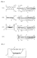
- Figure 1 shows an arranging method of a first embodiment of the invention using a positioning guide.
- reference numeral 1 designates a V-groove substrate
- 2 designates a positioning guide
- 4 and 5 designate fiber ribbons
- 6 and 6' designate bare fibers.
- the upper bare fibers 6' are shown with double circles.
- a positioning guide 2 is provided with a recess portion having inclined wall surfaces such that an opening is wider than a bottom width, and the size of the bottom is determined so as to become equal to the whole width of bare fibers in an arrayed state.
- a positioning guide 3 presses the bare fibers toward the bottom of the recess portion of the positioning guide 2.
- the V-groove substrate 1 and the bare fibers 6 are relatively moved, the bare fibers 6 are put on V grooves of the V-groove substrate 1, and the bare fibers 6 are fixed to the V-groove substrate 1 by a suitable method, for example, the bare fibers are bonded to the V-groove substrate 1 in a state where the bare fibers 6 are pressed to the V grooves by using a not-shown fiber pressing member, so that an optical fiber array is made.
- the V-groove substrate 1 may be raised, or the holding member of the two fiber ribbons 4 and 5 and the positioning guides 2 and 3 may be moved downward together.
- Figure 3 shows an example of a method of alternately arranging the respective fibers 6 of the two fiber ribbons 4 and 5.
- the coating of the end portions of the two fiber ribbons 4 and 5 are removed to expose the bare fibers 6, as shown in Fig. 3, if the fiber ribbons 4 and 5 are put so that the respective bare fibers 6 vertically cross each other at about their root portions, it is possible to alternately arrange the respective bare fibers 6 of the two fiber ribbons 4 and 5 easily.
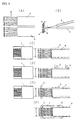
- FIGs 4, 5A and 5B are explanatory views for explaining a second embodiment of a method of making an optical fiber array of the invention.
- the same portions as those of Figs. 1 and 2 are designated by the same reference numerals, and their explanation will be omitted.
- positioning guides 2 and 3 are different from those of the embodiment described in Figs. 1 and 2.
- both the positioning guides 2 and 3 include recess portions each having inner walls inclined such that the bottom portion is narrower than the opening portion. Both the recess portions may have the same shape and size as the positioning guide 2 described in Figs. 1 and 2.
- bare fibers 6 As shown in Fig. 5A, with respect to bare fibers 6' arranged in an irregular state, the two positioning guides 2 and 3 are brought into contact so as to rub each other, and the positioning guides 2 and 3 are moved so that the bare fibers are put between the two positioning guides 2 and 3. As a result, the bare fibers 6 can be arrayed as shown in Fig. 5B.
- a fixing method of the arrayed bare fibers 6 to the V-groove substrate is the same as the fixing method in the first embodiment described in Fig. 1 and Fig. 2.
- the inclined surfaces of the recess portions of both the positioning guides 2 and 3 move the bare fibers from the right and left, and the bottom portions of the recess portions press the bare fibers from above and below, so that the bare fibers can be arrayed while being guided.
- Figures 6A to 6D are explanatory views for explaining a third embodiment of a method of making an optical fiber array of the invention.
- the same portions as those of Fig. 2 are designated by the same reference numerals and their explanation will be omitted.
- Figures 6A to 6D are views for explaining a process of arraying bare fibers.
- the right side of each drawing is a side view and the left side of each view is a front view of a positioning guide (front view is omitted in Fig. 6D).
- Reference numerals 2, 3a and 3b designate positioning guides.
- the positioning guides 3a and 3b functioning to press the bare fibers in the up and down direction, that is, from the direction orthogonal to the arrangement plane of the bare fibers, and the positioning guide 2 functioning to move the bare fibers in the horizontal direction along the arrangement plane, that is, from both sides of the arrangement direction of the bare fibers are structured by different members.
- the positioning guide 2 is provided with a recess portion, and inclined surfaces are formed at both sides of the recess portion. This reces portion may have the same shape and size as the recess portion of the positioning guide 2 described in Figs. 1 and 2.
- Figure 6A shows a state in which coating of the tip portions of the fiber ribbons 4 and 5 are removed so that the bare fibers 6 are exposed.
- the respective bare fibers of the fiber ribbons 4 and 5 are placed to be alternately positioned, as explained in Fig. 3, respective bare fibers of the upper and lower fiber ribbons are put to vertically cross each other so as to be alternately arranged.
- the positioning guides 3a and 3b press the bare fibers while holding the bare fibers from above and below.
- the pressing of the bare fibers by the positioning guides 3a and 3b is carried out with moderate strength. Since it is necessary to allow movement of the bare fibers 6 in the pressed state, pressing of the bare fibers 6 is carried out in such a manner that an interval larger than the outer diameter of the bare fiber 6 is maintained between the positioning guides 3a and 3b. However, if such interval is too large, the arrangement of the alternately arranged bare fibers 6 is disturbed, so that the interval of the positioning guides 3a and 3b is smaller than a value twice the outer diameter of the bare fiber 6.
- the interval of the positioning guides 3a and 3b in a pressing state is at a degree such that it is larger than 125 ⁇ m and less than 150 ⁇ m.
- Intervals between the bare fibers 6 are regulated. As shown in Fig. 6C, the positioning guide 2 is raised. The bare fibers 6 are moved by the inclined surfaces at both sides of the recess portion of the positioning guide 2, so that adjacent bare fibers are arranged to be brought into almost close contact, and the intervals between the bare fibers 6 are made uniform.
- the arranged bare fibers 6 are made to go down so as to be positioned on the V-groove substrate 1.
- the V-groove substrate 1 may be raised.
- the bare fibers 6 can be arranged on individual V grooves of the V-groove substrate 1.
- Figure 7 is an explanatory view of an operation of the positioning guide.
- the positioning guide 2 When the positioning guide 2 is relatively moved to the bare fibers 6' placed at uneven intervals, they are moved through the inclined surfaces and the intervals can be unified as indicated by the bare fibers 6.
- the positioning guide 2 is not limited to the use of the inclined surfaces. Since the bare fibers have only to be moved, a mechanism for holding the bare fibers between two guides from both sides may be used like the positioning guides 3a and 3b described in Figs. 6A to 6D.
- arraying of bare fibers is carried out through image processing, and is basically the same as the process described in Figs. 6A to 6D.
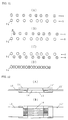
- Figure 8A shows a state in which a coating with a predetermined length at the tip portion of each of fiber ribbons 4 and 5 is removed so that bare fibers 6 are exposed.
- the respective fiber ribbons 4 and 5 in which the bare fibers 6 are exposed are held by holding means capable of obtaining position information, for example, holding means capable of detecting an amount of three-dimensional movement as digital data.
- a suitably determined initial position is made a standard, and a movement amount or deviation amount of the fiber ribbons 4 and 5 is obtained as position information with digital data.
- FIG. 9 shows an example of the image pickup means.
- part of the bare fibers is displayed on the basis of the image pickup data by using a display screen of a CCD monitor, and image processing is performed at two positions so that observed data are taken. Two observation positions are indicated by a P line and a Q line.
- data of the position of the holding means with respect to the position of the CCD, the length m of the bare fiber, and the length n from the observation position P to the tip of the bare fiber arithmetic processing is carried out, to obtain position information of the tip position and root position of each bare fiber.
- the position information of the fiber ribbons at the time of image pickup may be used as the initial position standard mentioned above.
- the tip position of a specific bare fiber may be used as the initial position standard.
- the intervals are intervals of adjacent centers of the tips of the upper and lower bare fibers, for example, an interval seen in orthogonal projection (orthogonal projection to the arrangement plane of the bare fibers ) of the tips of the bare fibers 4a and 5a, an interval seen from orthogonal projection of the tips of the bare fibers 4a and 5b, and so on.
- an interval seen in orthogonal projection (orthogonal projection to the arrangement plane of the bare fibers ) of the tips of the bare fibers 4a and 5a an interval seen from orthogonal projection of the tips of the bare fibers 4a and 5b, and so on.
- Figure 11A is a view showing the tips of the bare fibers shown in Fig. 10B.
- the holding means is driven to give a movement amount ⁇ to the upper fiber ribbon 4 with respect to the position of the tip of the bare fiber 5a as the standard position, so that, as shown in Fig. 11B, the tips of the upper and lower bare fibers are alternately disposed (in the case where the tips of the upper and lower bare fibers cannot be alternately arranged even if the movement amount ⁇ is changed, the case is made an error as described above).
- Fig. 11B the tips of the upper and lower bare fibers are alternately disposed (in the case where the tips of the upper and lower bare fibers cannot be alternately arranged even if the movement amount ⁇ is changed, the case is made an error as described above).
- Figure 8C is a view showing the arrayed state seen on a plane. In this state, the position of each bare fiber does not correspond to the position of each V groove of the V-groove substrate 1.
- the lower fiber ribbon 5 is moved so that the roots of the bare fibers of the lower fiber ribbon 5 to be set are positioned on the extensions of the respective V grooves of the V-groove substrate 1.
- the upper fiber ribbon 4 is also moved in the same manner.
- the fiber ribbon 4 and the fiber ribbon 5 become a state such that they overlap together from the tip to the root at the position shifted by about a half pitch. Either step of Figs. 8D and 8E may be performed first.
- the lower fiber ribbon is moved and the root positions of the bare fibers are adjusted.
- the root positions of the bare fibers may be adjusted after the upper fiber ribbon is first moved.
- adjustment of the root positions of the upper and lower fiber ribbons may be carried out after the positions of the tip portions of the bare fibers are adjusted by the positioning guide.
- the root positions of the bare fibers in the respective fiber ribbons are not necessarily arranged at completely equal intervals. Besides, in the removing operation of coating, a case can also occur where the root positions of the bare fibers are changed.
- the fiber ribbon 5 is moved with the bare fiber 5a as a standard, or the case where the fiber ribbon 4 is moved with the bare fiber 4a as a standard, when a fiber ribbon is moved with the root position of one bare fiber in the fiber ribbon as a standard, there is a case where an amount of movement is not necessarily suitable.
- the standard position of the respective fiber ribbons may be determined by arithmetic processing such as calculation of a mean value or least-square method.
- the movement of the fiber ribbons 4 and 5 is made such that the bare fibers of the upper and lower fiber ribbons 4 and 5 become parallel to the V grooves of the V-groove substrate 1.
- the positions of the roots of the bare fibers in the respective fiber ribbons are not necessarily arranged at an equal interval and at the same pitch completely equivalent to the outer diameter of the bare fiber, and the outer diameter of the bare fiber also has tolerance.
- the bare fibers automatically set in the V grooves from receiving external damage at the time of setting of the fibers they may be set over the whole length of the V grooves in parallel to the V grooves.
- the invention is not limited to this.
- pairs of fiber ribbons overlapped up and down are arranged in parallel and an optical fiber array using four fiber ribbons may be made, and further, the number of pairs arranged in parallel may be increased.
- the invention is not limited to the case where the fiber ribbons are overlapped together, but one fiber ribbon may be used. In that case, the pitch of V grooves is twice that of the foregoing embodiments. Even in the structure where one fiber ribbon is used, a plurality of fiber ribbons may be arranged in parallel.
- optical fiber includes a fiber ribbon and a single core fiber.
Landscapes
- Physics & Mathematics (AREA)
- General Physics & Mathematics (AREA)
- Optics & Photonics (AREA)
- Mechanical Coupling Of Light Guides (AREA)
- Optical Couplings Of Light Guides (AREA)
Applications Claiming Priority (2)
| Application Number | Priority Date | Filing Date | Title |
|---|---|---|---|
| JP25554298 | 1998-09-09 | ||
| JP25554298 | 1998-09-09 |
Publications (3)
| Publication Number | Publication Date |
|---|---|
| EP0985943A2 true EP0985943A2 (de) | 2000-03-15 |
| EP0985943A3 EP0985943A3 (de) | 2001-11-07 |
| EP0985943B1 EP0985943B1 (de) | 2006-11-15 |
Family
ID=17280184
Family Applications (1)
| Application Number | Title | Priority Date | Filing Date |
|---|---|---|---|
| EP99117707A Expired - Lifetime EP0985943B1 (de) | 1998-09-09 | 1999-09-08 | Verfahren zur Herstellung eines faseroptischen Arrays und Vorrichtung zur Herstellung eines faseroptischen Arrays |
Country Status (4)
| Country | Link |
|---|---|
| US (1) | US6299361B1 (de) |
| EP (1) | EP0985943B1 (de) |
| KR (1) | KR20000022972A (de) |
| CN (1) | CN1247990A (de) |
Cited By (4)
| Publication number | Priority date | Publication date | Assignee | Title |
|---|---|---|---|---|
| WO2002044782A3 (en) * | 2000-11-28 | 2003-04-03 | Lightwave Microsystems Corp | Assembly and method for reorganizing planar lightwave circuit channels |
| WO2003098307A1 (fr) * | 2002-05-17 | 2003-11-27 | Sumitomo Electric Industries, Ltd. | Coeur de fibre optique de type ruban, procede de production correspondant, connecteur portant un coeur de type ruban, ensemble de fibres optiques portant un coeur de type ruban et systeme de cablage optique |
| EP1215517A3 (de) * | 2000-12-14 | 2004-10-13 | Ngk Insulators, Ltd. | Optische Fasermatrixanordnung und Lichtwellenleitervorrichtung mit dieser Matrixanordnung |
| CN116165750A (zh) * | 2023-01-28 | 2023-05-26 | 中山市美速光电技术有限公司 | 一种用于生产可转换间距光纤阵列的制造系统 |
Families Citing this family (15)
| Publication number | Priority date | Publication date | Assignee | Title |
|---|---|---|---|---|
| US20030174998A1 (en) * | 2002-03-15 | 2003-09-18 | George Shevchuk | Assembly for stacking optical fibers in an aligned two dimensional array |
| US6885806B2 (en) * | 2002-07-19 | 2005-04-26 | Photonic Manufacturing Service Ltd. | Method of making an optical fiber array by overlapping stripped portions of ribbon fibers |
| KR20040020249A (ko) * | 2002-08-30 | 2004-03-09 | 우리로광통신주식회사 | 광섬유 어레이의 제조장치 |
| JP3764446B2 (ja) * | 2003-06-30 | 2006-04-05 | Tdk株式会社 | 光伝送モジュールの接続方法および装置、および光導波路におけるコア位置検出方法 |
| JP2005202164A (ja) * | 2004-01-15 | 2005-07-28 | Omron Corp | 光ファイバ保持部材及びその製造方法 |
| US7158712B2 (en) * | 2005-05-06 | 2007-01-02 | Coretech Optical Co., Ltd. | Optical fiber coupler and manufacturing apparatus and method thereof |
| US7756382B2 (en) * | 2005-06-30 | 2010-07-13 | Corning Cable Systems Llc | Optical fiber splitter module and fiber optic array therefor |
| JP2007072080A (ja) * | 2005-09-06 | 2007-03-22 | Fujikura Ltd | 光ファイバ端部の保持装置及びその方法 |
| TWI531111B (zh) * | 2014-02-14 | 2016-04-21 | Univ Chung Hua | Low crosstalk high frequency transmission differential pair microstrip line |
| JP6972904B2 (ja) * | 2017-10-19 | 2021-11-24 | 住友電気工業株式会社 | 光ファイバケーブル、光コネクタケーブル、及び、光ファイバケーブルの製造方法 |
| CN107643573B (zh) * | 2017-10-26 | 2024-08-02 | 江苏亨通光电股份有限公司 | 一种光纤带制作方法以及光纤夹具体装置 |
| US11415754B2 (en) * | 2019-09-30 | 2022-08-16 | Corning Incorporated | Fiber array spacers, optical assemblies incorporating fiber array spacers, and methods of fabricating the same |
| US10908362B1 (en) | 2019-10-16 | 2021-02-02 | International Business Machines Corporation | Interlacing boot for two-row ferrule ribbon for one dimensional photonic chip beach front |
| US12068791B2 (en) * | 2020-07-24 | 2024-08-20 | Molex, Llc | Photonic chip coupler connector module |
| JP7844785B2 (ja) * | 2021-06-18 | 2026-04-14 | 住友電工オプティフロンティア株式会社 | 融着接続機、及び、光ファイバの接続方法 |
Family Cites Families (11)
| Publication number | Priority date | Publication date | Assignee | Title |
|---|---|---|---|---|
| JPS63163406A (ja) | 1986-12-26 | 1988-07-06 | Matsushita Electric Ind Co Ltd | 光フアイバアレイ |
| JPH03204606A (ja) * | 1990-01-04 | 1991-09-06 | Nippon Telegr & Teleph Corp <Ntt> | 光ファイバの取付方法 |
| JPH0659161A (ja) * | 1992-08-10 | 1994-03-04 | Nippon Telegr & Teleph Corp <Ntt> | 多心光ファイバのピッチ変換コネクタ |
| JP3170387B2 (ja) * | 1993-05-21 | 2001-05-28 | 京セラ株式会社 | 光ファイバを固定用v溝基板に固定する方法 |
| JPH0968629A (ja) | 1995-08-31 | 1997-03-11 | Furukawa Electric Co Ltd:The | 多心光コネクタ |
| JPH09230158A (ja) | 1996-02-21 | 1997-09-05 | Fujikura Ltd | 光ファイバの配列構造 |
| JPH09288224A (ja) * | 1996-04-22 | 1997-11-04 | Fujikura Ltd | 多心光ファイバのコア位置推定方法と調心方法 |
| JPH09325231A (ja) * | 1996-05-31 | 1997-12-16 | Furukawa Electric Co Ltd:The | 光ファイバの軸合わせ方法および光ファイバの軸合わせ用観測装置 |
| WO1998005989A1 (en) * | 1996-08-01 | 1998-02-12 | Furukawa Denki Kogyo Kabushiki Kaisha | Multicore optical connector and method of producing the connector |
| JP3398764B2 (ja) | 1996-09-19 | 2003-04-21 | 日本電信電話株式会社 | 光ファイバブロック組立装置および光ファイバブロック組立治具 |
| JP2958628B2 (ja) | 1997-04-16 | 1999-10-06 | 北日本電線株式会社 | 光ファイバアレイ組立装置、光ファイバアレイ組立及び接着加工装置、並びに光ファイバアレイの製造方法 |
-
1999
- 1999-09-08 EP EP99117707A patent/EP0985943B1/de not_active Expired - Lifetime
- 1999-09-08 US US09/391,387 patent/US6299361B1/en not_active Expired - Fee Related
- 1999-09-08 KR KR1019990038042A patent/KR20000022972A/ko not_active Withdrawn
- 1999-09-09 CN CN99118583A patent/CN1247990A/zh active Pending
Cited By (6)
| Publication number | Priority date | Publication date | Assignee | Title |
|---|---|---|---|---|
| WO2002044782A3 (en) * | 2000-11-28 | 2003-04-03 | Lightwave Microsystems Corp | Assembly and method for reorganizing planar lightwave circuit channels |
| EP1215517A3 (de) * | 2000-12-14 | 2004-10-13 | Ngk Insulators, Ltd. | Optische Fasermatrixanordnung und Lichtwellenleitervorrichtung mit dieser Matrixanordnung |
| WO2003098307A1 (fr) * | 2002-05-17 | 2003-11-27 | Sumitomo Electric Industries, Ltd. | Coeur de fibre optique de type ruban, procede de production correspondant, connecteur portant un coeur de type ruban, ensemble de fibres optiques portant un coeur de type ruban et systeme de cablage optique |
| US8811783B2 (en) | 2002-05-17 | 2014-08-19 | Sumitomo Electric Industries, Ltd. | Tape-like optical fiber core, production method therefor, tape core-carrying connector, tape core-carrying optical fiber array, and optical wiring system |
| CN116165750A (zh) * | 2023-01-28 | 2023-05-26 | 中山市美速光电技术有限公司 | 一种用于生产可转换间距光纤阵列的制造系统 |
| CN116165750B (zh) * | 2023-01-28 | 2023-06-27 | 中山市美速光电技术有限公司 | 一种用于生产具有不同间距的光纤阵列的制造系统 |
Also Published As
| Publication number | Publication date |
|---|---|
| KR20000022972A (ko) | 2000-04-25 |
| EP0985943B1 (de) | 2006-11-15 |
| CN1247990A (zh) | 2000-03-22 |
| US6299361B1 (en) | 2001-10-09 |
| EP0985943A3 (de) | 2001-11-07 |
Similar Documents
| Publication | Publication Date | Title |
|---|---|---|
| EP0985943B1 (de) | Verfahren zur Herstellung eines faseroptischen Arrays und Vorrichtung zur Herstellung eines faseroptischen Arrays | |
| JP3105624B2 (ja) | 多心コネクタおよびその製造法 | |
| US7850372B2 (en) | Optical connector with optical fiber | |
| JP3738441B2 (ja) | 光ファイバー用受動整列接続装置 | |
| CN113589448A (zh) | 高密度fau和光学互连设备以及相关方法 | |
| JP3273490B2 (ja) | 多芯マイクロキャピラリとこれを用いた光導波回路と光ファイバとの接続方法 | |
| JPH09178962A (ja) | 光ファイバアレイおよびその製造法 | |
| JP2004078028A (ja) | 光ファイバガイド部品およびその作製方法 | |
| EP0200414B1 (de) | Vorrichtung und Verfahren zum Abschluss optischer Fasern | |
| JP2005517966A (ja) | 高密度光ファイバーアレイ | |
| KR20020046950A (ko) | 파이버 어레이 및 도파로 디바이스 | |
| US6478473B1 (en) | Multiple-fiber optical connector, and method for assembling the same | |
| JPH10246838A (ja) | 光ファイバアレイ装置 | |
| JP3772929B2 (ja) | 光ファイバ保持部品および光ファイバアレイ | |
| JP3120807B2 (ja) | 光ファイバアレイの製造方法 | |
| US6618514B1 (en) | Passive pigtail attachment apparatus and method for planar lightwave circuits | |
| US6010249A (en) | Optical end piece and method for testing the coupling surface of an optical end piece | |
| JP4172097B2 (ja) | ロッドレンズ付き光ファイバ配列部品の製造方法 | |
| JP3968543B2 (ja) | 光ファイバアレイの製造方法 | |
| JPH09105838A (ja) | 光導波路装置 | |
| JP3221172B2 (ja) | 光結合装置 | |
| JP7795365B2 (ja) | 光コネクター、光モジュール、および光コネクターの評価方法 | |
| JP2565124B2 (ja) | アレイ光ファイバの整列構造 | |
| JP2000187131A (ja) | 光導波路モジュールの製造方法 | |
| JP2003194667A (ja) | 光ファイバ端面検査装置 |
Legal Events
| Date | Code | Title | Description |
|---|---|---|---|
| PUAI | Public reference made under article 153(3) epc to a published international application that has entered the european phase |
Free format text: ORIGINAL CODE: 0009012 |
|
| AK | Designated contracting states |
Kind code of ref document: A2 Designated state(s): AT BE CH CY DE DK ES FI FR GB GR IE IT LI LU MC NL PT SE Kind code of ref document: A2 Designated state(s): FR GB IT |
|
| AX | Request for extension of the european patent |
Free format text: AL;LT;LV;MK;RO;SI |
|
| PUAL | Search report despatched |
Free format text: ORIGINAL CODE: 0009013 |
|
| AK | Designated contracting states |
Kind code of ref document: A3 Designated state(s): AT BE CH CY DE DK ES FI FR GB GR IE IT LI LU MC NL PT SE |
|
| AX | Request for extension of the european patent |
Free format text: AL;LT;LV;MK;RO;SI |
|
| 17P | Request for examination filed |
Effective date: 20020103 |
|
| 17Q | First examination report despatched |
Effective date: 20020219 |
|
| AKX | Designation fees paid |
Free format text: FR GB IT |
|
| REG | Reference to a national code |
Ref country code: DE Ref legal event code: 8566 |
|
| GRAP | Despatch of communication of intention to grant a patent |
Free format text: ORIGINAL CODE: EPIDOSNIGR1 |
|
| GRAS | Grant fee paid |
Free format text: ORIGINAL CODE: EPIDOSNIGR3 |
|
| GRAA | (expected) grant |
Free format text: ORIGINAL CODE: 0009210 |
|
| AK | Designated contracting states |
Kind code of ref document: B1 Designated state(s): FR GB IT |
|
| REG | Reference to a national code |
Ref country code: GB Ref legal event code: FG4D |
|
| ET | Fr: translation filed | ||
| PLBE | No opposition filed within time limit |
Free format text: ORIGINAL CODE: 0009261 |
|
| STAA | Information on the status of an ep patent application or granted ep patent |
Free format text: STATUS: NO OPPOSITION FILED WITHIN TIME LIMIT |
|
| 26N | No opposition filed |
Effective date: 20070817 |
|
| PGFP | Annual fee paid to national office [announced via postgrant information from national office to epo] |
Ref country code: GB Payment date: 20120905 Year of fee payment: 14 |
|
| PGFP | Annual fee paid to national office [announced via postgrant information from national office to epo] |
Ref country code: FR Payment date: 20120926 Year of fee payment: 14 Ref country code: IT Payment date: 20120810 Year of fee payment: 14 |
|
| GBPC | Gb: european patent ceased through non-payment of renewal fee |
Effective date: 20130908 |
|
| REG | Reference to a national code |
Ref country code: FR Ref legal event code: ST Effective date: 20140530 |
|
| PG25 | Lapsed in a contracting state [announced via postgrant information from national office to epo] |
Ref country code: GB Free format text: LAPSE BECAUSE OF NON-PAYMENT OF DUE FEES Effective date: 20130908 |
|
| PG25 | Lapsed in a contracting state [announced via postgrant information from national office to epo] |
Ref country code: IT Free format text: LAPSE BECAUSE OF NON-PAYMENT OF DUE FEES Effective date: 20130908 Ref country code: FR Free format text: LAPSE BECAUSE OF NON-PAYMENT OF DUE FEES Effective date: 20130930 |