EP0986094A2 - Méthode d'exposition, et méthode de fabrication de dispositifs utilisant cette méthode d'exposition - Google Patents
Méthode d'exposition, et méthode de fabrication de dispositifs utilisant cette méthode d'exposition Download PDFInfo
- Publication number
- EP0986094A2 EP0986094A2 EP99307119A EP99307119A EP0986094A2 EP 0986094 A2 EP0986094 A2 EP 0986094A2 EP 99307119 A EP99307119 A EP 99307119A EP 99307119 A EP99307119 A EP 99307119A EP 0986094 A2 EP0986094 A2 EP 0986094A2
- Authority
- EP
- European Patent Office
- Prior art keywords
- pattern
- exposure
- region
- fine pattern
- substrate
- Prior art date
- Legal status (The legal status is an assumption and is not a legal conclusion. Google has not performed a legal analysis and makes no representation as to the accuracy of the status listed.)
- Withdrawn
Links
Images


Classifications
-
- G—PHYSICS
- G03—PHOTOGRAPHY; CINEMATOGRAPHY; ANALOGOUS TECHNIQUES USING WAVES OTHER THAN OPTICAL WAVES; ELECTROGRAPHY; HOLOGRAPHY
- G03F—PHOTOMECHANICAL PRODUCTION OF TEXTURED OR PATTERNED SURFACES, e.g. FOR PRINTING, FOR PROCESSING OF SEMICONDUCTOR DEVICES; MATERIALS THEREFOR; ORIGINALS THEREFOR; APPARATUS SPECIALLY ADAPTED THEREFOR
- G03F7/00—Photomechanical, e.g. photolithographic, production of textured or patterned surfaces, e.g. printing surfaces; Materials therefor, e.g. comprising photoresists; Apparatus specially adapted therefor
- G03F7/20—Exposure; Apparatus therefor
- G03F7/2022—Multi-step exposure, e.g. hybrid; backside exposure; blanket exposure, e.g. for image reversal; edge exposure, e.g. for edge bead removal; corrective exposure
-
- H—ELECTRICITY
- H10—SEMICONDUCTOR DEVICES; ELECTRIC SOLID-STATE DEVICES NOT OTHERWISE PROVIDED FOR
- H10P—GENERIC PROCESSES OR APPARATUS FOR THE MANUFACTURE OR TREATMENT OF DEVICES COVERED BY CLASS H10
- H10P76/00—Manufacture or treatment of masks on semiconductor bodies, e.g. by lithography or photolithography
-
- G—PHYSICS
- G03—PHOTOGRAPHY; CINEMATOGRAPHY; ANALOGOUS TECHNIQUES USING WAVES OTHER THAN OPTICAL WAVES; ELECTROGRAPHY; HOLOGRAPHY
- G03F—PHOTOMECHANICAL PRODUCTION OF TEXTURED OR PATTERNED SURFACES, e.g. FOR PRINTING, FOR PROCESSING OF SEMICONDUCTOR DEVICES; MATERIALS THEREFOR; ORIGINALS THEREFOR; APPARATUS SPECIALLY ADAPTED THEREFOR
- G03F7/00—Photomechanical, e.g. photolithographic, production of textured or patterned surfaces, e.g. printing surfaces; Materials therefor, e.g. comprising photoresists; Apparatus specially adapted therefor
- G03F7/70—Microphotolithographic exposure; Apparatus therefor
- G03F7/70425—Imaging strategies, e.g. for increasing throughput or resolution, printing product fields larger than the image field or compensating lithography- or non-lithography errors, e.g. proximity correction, mix-and-match, stitching or double patterning
- G03F7/70466—Multiple exposures, e.g. combination of fine and coarse exposures, double patterning or multiple exposures for printing a single feature
Definitions
- This invention relates generally to an exposure method. More particularly, the invention is concerned with an exposure method wherein a first exposure process as can be represented by a standard or ordinary exposure process, such as projection exposure, and a second exposure process of higher resolving power than the first exposure process, are performed so that different types of patterns are printed superposedly to thereby form a desired pattern (hereinafter "goal pattern") of smallest linewidth corresponding to the second exposure process.
- the present invention is suitably applicable to manufacture of chips or devices such as semiconductor chips (e.g., ICs or LSIs), detecting devices (e.g., magnetic heads), micro-machines or image pickup devices (e.g., CCDs), for example.
- NA numerical aperture
- the numerical aperture (NA) of a projection optical system may be enlarged or the wavelength of exposure light may be shortened. Practically, however, enlargement of the NA or reduction in wavelength of the exposure light is not very easy.
- the depth of focus of a projection optical system is inversely proportional to the square of the NA while it is proportional to the wavelength ⁇ . Because of this, enlarging the NA of a projection optical system results in a decrease of the depth of focus, which causes a difficulty of focusing and a decrease of productivity. Further, most glass materials have an extraordinarily low transmission factor with respect to a deep ultraviolet region.
- Japanese Patent Application, Application No. 304232/1997 (hereinafter, "the earlier Japanese patent application"), filed by the assignee of the subject application, proposes a dual exposure process which is based on a combination of dual-beam interference exposure and standard exposure, wherein a multiple-value exposure amount distribution is applied to a substrate, to be exposed, to assure high resolution exposure.
- the dual-beam interference exposure process is performed by use of a phase shift mask having a line-and-space (L&S) pattern of 0.1 micron linewidth, and a fine linear pattern is printed through coherent illumination.
- L&S line-and-space
- an ordinary exposure process for example, an exposure process based on partially coherent illumination
- a mask which is formed with a pattern having portions of different transmission factors and having a shape corresponding to an actual device pattern of smallest linewidth of 0.1 micron.
- a pattern of smallest linewidth of 0.10 micron may be formed through the ordinary exposure process and by using a projection exposure apparatus having a projection optical system which has an image side NA of 0.6.
- Another method for the fine pattern printing is a probe exposure method wherein a pattern is drawn and printed on a photosensitive member by using a probe.
- the probe may be based on AFM using an interatomic force, STM using a tunnel current, an electron beam, a laser beam or proximity light, for example.
- performing the probe exposure over the whole exposure area has a disadvantage of low throughput.
- those portions of a goal pattern that can be produced through an ordinary exposure process may be photoprinted by using a light quantity larger than an exposure threshold of a photosensitive substrate.
- those portions of insufficient resolution may be photoprinted by superposed printing which is based on an ordinary exposure and a probe exposure, with the respective light quantities each being lower than the exposure threshold of the photosensitive material but both, when combined, being higher than the exposure threshold.
- a multiple-value exposure amount distribution similar to that described above is applied (Japanese Patent Application, Application No. 137476/1998).
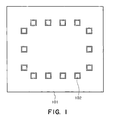
- Figure 1 is a schematic view for explaining an example of the structure of a semiconductor chip, according to an embodiment of the present invention.
- Figure 2 is a schematic view for explaining an example of the structure of an output buffer circuit in the semiconductor chip of Figure 1.
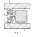
- Figure 3 is a schematic view for explaining an example of the structure of an input buffer circuit of the semiconductor chip of Figure 1.
- Figure 4 is a schematic view for explaining an example of the shape and structure of a fine linear pattern which can be used for formation of a fine pattern corresponding to the output and input buffer circuits of the semiconductor chip of Figure 1.
- Figure 5 is a schematic view for explaining the state of exposure, in a case where a fine linear periodic pattern region and a goal pattern region coincide with each other.
- Figure 6 is a schematic view for explaining the state of exposure, in a case where a fine linear periodic pattern region is magnified, as compared with a goal pattern region, in opposite directions along the direction of array of the fine linear pattern and by an amount corresponding to four lines of the fine linear pattern.
- Figures 7A and 7B are graphs, respectively, for explaining the width of exposure amount that can be resolved by the dual exposure method of Figures 5 and 6.
- Figure 8 is a graph for explaining the relation between the length of a pattern to be formed through the dual exposure and an increase in length where a fine linear pattern is enlarged in the lengthwise direction beyond a goal pattern region.
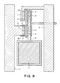
- Figure 9 is a schematic view for explaining an example of the structure where the angle of the output buffer circuit in the semiconductor chip of Figure 1 differs from that of Figure 3 by 90 deg.
- Figure 10 is a schematic view for explaining an example of the structure of a pad portion in a semiconductor chip according to a second embodiment of the present invention.
- Figure 11 is an enlarged view of an upper right portion of the semiconductor chip of Figure 10.
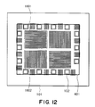
- Figure 12 is a schematic view for explaining an example where a fine pattern is placed inside a semiconductor chip.
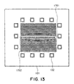
- Figure 13 is a schematic view for explaining another example where a fine pattern is placed inside a semiconductor chip.
- Figure 14 is a schematic view for explaining a further example where a fine pattern is placed inside a semiconductor chip, together with a void portion.
- Figure 15 is a schematic view for explaining an example of the structure of a matrix type photoelectric converting device, which can be produced in accordance with a multiple exposure process of the present invention.
- Figure 16 is a schematic view for explaining an example of the layout of a fine linear pattern, for forming a fine pattern of a chip-inside-device, in the device of Figure 15.
- Figures 17A, 17B and 17C are schematic views, respectively, for explaining a process for forming a silicon active region.
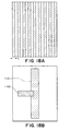
- Figures 18A and 18B are schematic views, respectively, for explaining the principle of dual exposure process.
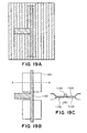
- Figures 19A, 19B and 19C are schematic views, respectively, for explaining the principle of dual exposure process.
- Figures 20A and 20B are schematic views, respectively, for explaining an exposure pattern in fine linear exposure.
- Figures 21A and 21B are schematic views, respectively, for explaining an exposure pattern in dual exposure, corresponding to a portion without a rough pattern.
- Figures 22A and 22B are schematic views, respectively, for explaining an exposure pattern in ordinary projection exposure.
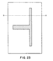
- Figure 23 is a schematic view of an example of a mask to be used for dual exposure by which a defocused image is superposed.
- Figures 24A, 24B, 24C and 24D are schematic views, respectively, for explaining an exposure pattern to be formed through dual exposure.
- Figures 25A and 25B are schematic views, respectively, for explaining the principle of triple exposure for forming a contact region.
- Figures 26A, 26B and 26C are schematic views, respectively, for explaining the principle of the triple exposure.
- Figures 27A, 27B and 27C are schematic views, respectively, for explaining the procedure for forming a wiring region.
- Figure 28 is a flow chart for explaining the procedure for manufacturing a microdevice.
- Figure 29 is a flow chart for explaining details of a wafer process, included in the procedure of Figure 28.
- a fine pattern and a pattern (hereinafter “rough pattern") having a smallest linewidth (upon a substrate) larger than that of the fine pattern, are printed on the substrate superposedly, by which a goal pattern having a smallest linewidth corresponding to that of the fine pattern, is formed on the substrate.
- This exposure method is called in this specification a “dual exposure” or “multiple exposure”.
- the region on which the fine pattern is to be printed is exposed with a size that contains the whole chip-inside-device forming region, upon one chip to be produced on a substrate, where a chip-inside-device is to be formed.
- chip-inside-device forming region refers to such region that includes all of or any one of (i) an active element such as an MOS transistor, a bipolar transistor or a diode, for example, (ii) a passive element such as a resistance element or a capacitance element, for example, and (iii) a connection region for electrical connection of the active element or the passive element.
- an active element such as an MOS transistor, a bipolar transistor or a diode
- a passive element such as a resistance element or a capacitance element, for example
- connection region for electrical connection of the active element or the passive element.
- a fine pattern should desirably be uniform as much as possible.
- a fine-pattern exposure region is made larger than a chip-inside-device forming region. This enables that a portion not influenced by a micro-loading effect, a proximity effect or an edge effect of the edge of the fine pattern, that is, a portion where the fine pattern is uniform in shape, is used in the chip-inside-device forming region.
- the exposure amount distribution control in a wide range as well as the state after the resist exposure e.g., oxide diffusion
- the time from the exposure to the development has a large influence to the linewidth (CD), this can be made uniform.
- the fine pattern in the chip-inside-device forming region can be made uniform through the procedure described above.
- the reproducibility of a goal can therefore be improved, and thus various devices such as a semiconductor chip, for example, can be manufactured very precisely.
- a semiconductor chip is provided with pads at its outer peripheral portion, for transmission and reception of signals to and from the outside of the chip.
- Figure 1 shows an example, wherein denoted at 101 is a semiconductor chip which is formed on a semiconductor wafer or substrate, and denoted at 102 are pads formed at the outer peripheral portion of the chip. For transmission and reception of a greater amount of information, there are cases where pads are formed along all the four peripheral sides of the chip, such as shown in the drawing.
- such a semiconductor chip has output pads each having a buffer circuit to which a single-stage or multiple-stage inverter circuit (signal inverting circuit) for driving a large load outside the chip is connected. Also, its input pads have a buffer circuit for driving the inside circuit.
- Figure 2 illustrates an example of an output pad having an output buffer circuit.
- a pad with a single-stage inverter buffer circuit For convenience in explanation, an example of a pad with a single-stage inverter buffer circuit will be described.
- Denoted in Figure 2 at 10 is a P type MOS transistor.
- Denoted at 1 is a source region of the P type MOS transistor, and denoted at 2 is a drain region of the P type MOS transistor.
- Denoted at 20 is an N type MOS transistor.
- Denoted at 3 is a source region of the N type MOS transistor, and denoted at 4 is a drain region of the N type MOS transistor.
- Denoted at 5 is a gate electrode which is used for both of the P type and N type MOS transistors.
- Denoted at 6 are contacts for connecting the sources and drain regions 1 - 4 with a wiring layer (wire 8, electric source wire 9 and ground wire 11).
- Denoted at 7 is a pad for connecting the semiconductor chip with the outside.
- the drain regions 2 and 4 are connected to the wire 8 through the contacts 6, and the wire 8 is connected to the pad 7.
- the source region 1 of the P type MOS transistor 10 is connected to the electric source wire 9 through the contact 6.
- the source region 3 of the N type MOS transistor 20 is connected to the ground wire 11 through the contact 6.
- the sources and drain regions 1 - 4 are defined in a silicon active layer at the surface of the silicon substrate, and the wiring layer is formed on an insulating layer (not shown) which is provided on the silicon active layer.
- the gate electrode 5 is provided by a polysilicone layer, a polycide layer or an accumulation of these layers.
- the P type MOS transistor 10 and the N type MOS transistor 20 provide a CMOS inverter.
- an inversion signal thereof is outputted to the pad 7.
- Figure 3 illustrates an example of an input pad having an input buffer circuit.
- like numerals as those of Figure 2 are assigned to corresponding elements.
- the signal in response to application of a signal from the outside to the pad 7, the signal is transmitted to the gate electrode 5 through the gate wire 12, whereby a signal as being inverted by the CMOS inverter is transmitted to the inside circuit (not shown).
- Figure 4 illustrates an example of a pattern shape, upon a semiconductor wafer, of a fine linear pattern (a stripe-like fine pattern) in a case where a fine MOS transistor is to be produced in an output buffer circuit and an input buffer circuit of a semiconductor chip on the semiconductor wafer through a convenient process.
- the production is based on a multiple exposure method wherein a fine linear pattern and a rough pattern having a smallest linewidth, upon a semiconductor wafer or substrate (or as the same is printed on the semiconductor wafer), larger than that of the fine linear pattern are printed on the substrate superposedly, whereby a goal pattern having a smallest linewidth corresponding to that of the fine linear pattern is produced on the wafer.
- the pattern forming region for forming the fine linear pattern 401 includes input and output buffer circuits, and the whole surface thereof is formed (exposed) into a size slightly larger than a chip-inside-device forming region 404 of the semiconductor chip 101.
- chip-inside-device forming region refers to such region that includes all of or any one of (i) an active element such as an MOS transistor, a bipolar transistor or a diode, for example, (ii) a passive element such as a resistance element or a capacitance element, for example, and (iii) a connection region for electrical connection of the active element or the passive element.
- an active element such as an MOS transistor, a bipolar transistor or a diode
- a passive element such as a resistance element or a capacitance element, for example
- connection region for electrical connection of the active element or the passive element.
- it is the region of the semiconductor chip 101 that includes an inside circuit, a peripheral circuit and a connection region for connecting them.
- peripheral circuits shown in Figures 2 and 3 corresponds to a region including P type MOS transistor 10, N type MOS transistor 20, contacts 6 for connecting the transistors 10 and 20 with wires 8, 9 and 11, and a contact (not shown) for connecting the gate 5 ( Figure 3) of the MOS transistors 10 and 20 with the pad 7.
- the position of the chip-inside-device forming region is not restricted by the placement of the pad 102.
- a chip-inside-device forming region may be defined in a region between the pad and the outer periphery of the semiconductor chip. Also, the position of the pad is not limited to the proximity to the chip outside periphery. It may be placed close to the center of the chip.
- the pattern forming region for forming the fine linear (periodic) pattern 401 is defined by the whole surface exposure to a size notably larger than the chip-inside-device forming region of the semiconductor chip 101, which provides an input/output buffer circuit.
- the end portion of the fine linear pattern having a lower exposure amount or resolution is positioned outside the chip-inside-device forming region. Therefore, in the chip-inside-device forming region, only a portion of the fine pattern which is uniform in respect to shape can be used. This enables that not only the inside circuit portion of the chip 101 but also the input/output buffer circuit are produced very precisely.
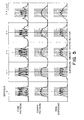
- Figures 5 and 6 illustrate a difference in respect to the setting of a fine periodic pattern region and a goal pattern (five-bar) region.
- Figure 5 shows an intensity distribution in the dual exposure in a case where the fine periodic pattern region is set in the same region as the goal pattern to be produced.
- Figure 6 shows an intensity distribution in the dual exposure in a case where the fine periodic pattern region is enlarged so that a goal pattern can be produced satisfactorily.
- the upper portion shows exposure amount distributions of a fine periodic pattern, using a Levenson type phase shift mask.
- the middle portion shows exposure amount distributions provided by a rough pattern.
- the lower portion shows exposure amount distributions provided by the dual exposure.
- the exposure amount distributions are illustrated in respect to various levels of defocus, varying along the lateral direction in the drawing. In these drawings, exposure amount distributions as well as the positions of the five bars are illustrated.
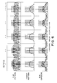
- Figures 7A and 7B show a resolvable exposure amount range.
- the region for the goal pattern coincides with the fine periodic pattern region, as shown in Figure 7A
- the five bars are resolved, the linewidth of each bar varies.
- the fine periodic pattern region is enlarged, as shown in Figure 7B, all the five bars can be resolved into a desired linewidth.
- Table 1 below shows preferable enlargement amounts (pattern bar number) of a fine periodic pattern, in a case where a projection exposure apparatus such as described above is used for the ordinary exposure process and the linewidth and spacing are set to 0.12 micron, 0.13 micron and 0.15 micron, respectively, and in a case where the number of bars of a goal pattern is set, in regard to isolated pattern, to one, three and five, respectively.
- the pattern bar number corresponds to the number of glass patterns in a case of a void pattern (the pattern is light transmissive) and to the number of Cr patterns in a case of a residual pattern (the pattern is light blocking).
- PATTERN WIDTH 0.12 0.13 0.15 PATTERN BAR NUMBER 1 3 2 1 3 4 3 2 >3 4 3 2
- the linewidth of a fine periodic pattern is 0.12 micron, it is effective in dual exposure to enlarge the fine periodic pattern region by four periodic pattern bars or more as compared with the goal pattern region.
- Figure 8 is a graph showing the increase in length of a fine periodic pattern (enlargement in the lengthwise direction) and the length of the pattern to be produced through the dual exposure.
- the smallest linewidth of the fine periodic pattern is w
- the length of a bar pattern to be formed through the dual exposure of a goal pattern (bar pattern) having a width w and a length 14w is illustrated in terms of percent (%).
- the lengthwise direction of the fine periodic pattern is the same as the goal pattern
- the length of a pattern produced as a result of dual exposure is shortened by about 14% as compared with the goal pattern.
- the fine periodic pattern is enlarged by 6 times the smallest linewidth (0.72 micron in case of smallest linewidth of 0.12 micron) or more.
- the fine periodic pattern exposure region should desirably be enlarged, at its opposite ends, by four bars or more with respect to the periodic direction as compared with the goal pattern region (device forming region), and be enlarged by 6 times or more the smallest linewidth with respect to the lengthwise direction.
- the pad in the region 402 may be formed in accordance with the layout such as shown in Figure 2 or 3.
- the orientation of the buffer circuit will be deviated from the pad by 90 deg. as shown in Figure 9.
- the length of the electric source wire 9 connecting the buffer circuit varies. This causes a difference in series resistance and, thus, a difference in operation speed of the buffer circuit.
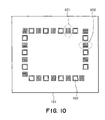
- Figure 10 illustrates an example of the structure of a pad in a semiconductor chip according to a second embodiment of the present invention.
- This embodiment is based on a multiple exposure method in which a fine linear pattern and a rough pattern having a smallest linewidth larger than the linewidth of the fine linear pattern are printed superposedly, such that a goal pattern having a smallest linewidth corresponding to the linewidth of the fine linear pattern is produced.
- there are plural fine linear patterns having at least two different angles.
- FIG 10 like numerals as those of Figure 1 are assigned to corresponding elements.
- Denoted in Figure 10 at 601 is a first fine linear pattern group
- denoted at 602 is a second fine linear pattern group which defines a right angle to the first fine linear pattern group 601.
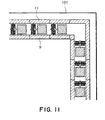
- Figure 11 is an enlarged view of the right upper portion of the chip of Figure 10.
- the orientation of the fine linear pattern may be changed in accordance with the placement of the pad, to thereby change the orientation of the MOS transistor. In this manner, a number of buffer circuits of uniform operation characteristic can be disposed in large integration.
- the present invention is not limited to pads, but it is applicable also to placement of transistors inside a semiconductor chip.
- Figures 12, 13 and 14 show examples wherein fine patterns are formed also inside a semiconductor chip.
- fine patterns may be formed throughout the whole surface of a fine-pattern exposure region.
- the patterns may be formed in the fine-pattern exposure region, except an inside portion thereof.
- denoted at 1801 is a void region without a fine linear pattern.
- plural fine linear pattern groups having different array directions may be formed.
- the first fine linear pattern 1601 or 1701 and the second fine linear pattern 1602 or 1702 are arrayed in orthogonal directions.
- Figure 15 shows an example wherein the concept of the second embodiment is applied to a matrix type photoelectric converting device which can be formed on a semiconductor wafer (substrate) as a single device.
- 801 is a photoelectric converting element region in which photoelectric converting elements are arrayed in matrix.
- 802 is a vertical scan circuit, and denoted at 803 is a horizontal scan circuit.
- 804 is a horizontal reading circuit, and denoted at 805 is an output amplifier.
- Electric charges as produced by photoelectric converting elements are directly read out by the horizontal reading circuit 804, or they are read out after being amplified by amplifying elements which are provided in association with the photoelectric converting elements, respectively, in an order as determined by the selection through the vertical scan circuit 802. After this, in the order as selected by the horizontal scan circuit 803, they are read out sequentially through the output amplifier 805.
- the vertical scan circuit 802 functions to perform sequential selection in vertical direction, and, for it, generally a combination of a CMOS inverter and a transfer switch or a combination of an N or P type MOS transistor and a capacitance element is known.
- the horizontal scan circuit 803 has a circuitry similar to that of the vertical scan circuit 802, but the scan direction thereof differs from that of the vertical scan circuit 802 by 90 deg. For this reason, in respect to large integration and efficient placement, it is necessary that the MOS transistors constituting the circuits 802 and 803 have orientations being different by 90 deg. from each other.
- Figure 16 shows the shape of a fine linear pattern for accomplishing the circuit of this embodiment.
- Denoted in the drawing at 901 is a first fine linear pattern group
- denoted at 902 is a second fine linear pattern group having its orientation different from the first fine linear pattern group by 90 deg.
- the first fine linear pattern group 901 is used to form a gate portion of an MOS transistor which constitutes the vertical scan circuit 802, while the second fine linear pattern group 902 is used to form a gate portion of an MOS transistor which constitutes the horizontal scan circuit 803. This enables efficient placement of circuits.
- a circuit which performs similar matrix driving is a liquid crystal display device, and, as a matter of course, similar advantageous results are attainable in that case.
- a decoder circuit may be used. Also in such case, similar advantageous results are obtainable. Further, similar advantageous results can be attained in cases of memories such as DRAM, SRAM, or flash memory, for example.
- this embodiment is applicable also to manufacture of mechanical devices such as a micromachine, for example, not only to a semiconductor device.
- Figures 17A through 25B are schematic views for explaining the procedure for manufacturing a chip-inside-device structure according to the present invention, on the basis of the multiple exposure method.
- Figures 17A - 17C show a process for forming a silicon active region.
- a silicon oxide film region may be formed outside that pattern by using a selection oxidation method (LOCOS), for example. This region may function as a device separation region, such that a silicon active region can be produced.
- LOC selection oxidation method
- Figure 17B is a plan view thereof, and Figure 17C is a sectional view taken along a line A - A' in Figure 17B.
- denoted at 1001 is a silicon active region which can thus be formed, and denoted at 1002 is a device separation region which comprises an electrically insulating layer.
- Figures 18A and 18B as well as Figures 19A - 19C illustrate the principle of dual exposure method for forming a gate region.
- Figure 18A shows a Levenson pattern having a linewidth and a spacing of L, as being printed on a semiconductor wafer.
- Figure 18B shows a rough pattern.
- the rough pattern comprises a pattern region 1101 having a transmission factor 1, and a pattern region 1102 having a transmission factor 2.
- the smallest linewidth and spacing of these pattern regions, as being printed on the semiconductor wafer, are set to 2L or more.
- the Levenson pattern and the rough pattern are photoprinted superposedly on a substrate as shown in Figure 19A, in accordance with the dual-beam interference exposure method and the standard or ordinary exposure method as described hereinbefore.
- the exposure threshold E th of the photoresist on which these patterns are printed as well as the patterns and the exposure amounts in the pattern regions are set in an appropriate relation with each other.
- a photoresist pattern such as a pattern 1103 shown in Figure 19B which corresponds to a gate having a smallest linewidth L, in the state being printed on the semiconductor wafer, can be produced.
- the transmission factors 1 and 2 are referred to only for convenience in explanation, and they have no specific physical significance.
- a gate insulation film may then be formed on the silicon active region 1001 ( Figures 17B and 17C) by thermal oxidation of the silicon. Thereafter, a polysilicon layer may be formed through a CVD (chemical vapor deposition) method, for example. The polysilicon layer may then be etched and patterned in accordance with the photoresist pattern having been formed through the dual exposure method described above, whereby a gate pattern of a smallest linewidth L can be formed.
- Figure 19B is a plan view of it
- Figure 19C is a sectional view taken along a line A - A' in Figure 19B.
- denoted at 1103 is a gate region of polysilicon, for example, and denoted at 1104 is a gate insulation film.
- Denoted at 1105 is are a source and a drain region of an MOS transistor, which are formed by impurity injection based on the ion injection method performed after the formation of the gate region 1103.
- FIGS 20A and 21A show a lithography pattern (nothing is produced), and Figures 20B and 21B show the relation between the exposure amount distribution and the exposure threshold.
- the reference character E 1 in Figures 20B and 21B denotes the exposure amount in the periodic pattern exposure, and the reference character E 2 denotes the exposure amount in the ordinary projection exposure.
- the dual exposure process has a feature that an exposure pattern of high resolution which may apparently disappear only through the periodic pattern exposure is mixed with an exposure pattern of desired shape, including a pattern of a size not larger than the resolving power of the ordinary projection exposure, such that only a desired portion of a resist is selectively exposed by an amount not lower than the exposure threshold of the resist, whereby a desired lithographic pattern can be finally produced.
- Figure 22A shows an exposure pattern provided by ordinary projection exposure.
- the resolution of ordinary projection exposure is set to be about a half of that of the dual-beam interference exposure for the periodic pattern exposure.
- the linewidth of the exposure pattern by the projection exposure as illustrated is about twice the linewidth of an exposure pattern by the dual-beam interference exposure.
- the total exposure amount distribution on the resist will be such as shown in the graph at the bottom of Figure 22B.
- the isolated linear pattern shown in the upper portion of Figure 22B has a resolution corresponding to that of the dual-beam interference exposure, and there is no simple periodic pattern.
- a high resolution pattern having a resolution higher than that as can be attained by the ordinary projection exposure is produced on the semiconductor wafer.
- Figure 23 shows a rough pattern mask with which a defocused image of a fine pattern, that can not be resolved by ordinary exposure, is superposed.
- This mask has a pattern directly corresponding to a gate having a smallest linewidth L, as being printed on a semiconductor wafer.
- Figure 24A shows an exposure pattern in the ordinary exposure
- Figure 24B shows the state of exposure corresponding to it. Since this exposure pattern is a fine pattern smaller than the resolving power of the exposure apparatus, it can not be resolved. Thus, the intensity distribution on the substrate being exposed is blurred and expanded.
- the exposure pattern comprises a fine pattern having a linewidth about a half of the resolution power of the ordinary projection exposure.
- the projection exposure for forming the exposure pattern of Figure 24C is performed, after the periodic pattern exposure of Figure 20A and without intervention of a development process, superposedly to the same region of the same resist. At that time, the center of the ordinary exposure pattern is registered with the peak of the periodic pattern. Then, the total exposure amount distribution on the resist will be such as shown in the graph of Figure 24D.
- the isolated linear pattern shown in Figure 24C has a resolution corresponding to that of the periodic pattern exposure, and a simple periodic pattern itself is not developed. Thus, a high resolution pattern having a resolution higher than that as can be attained by the ordinary projection exposure, is produced.
- the exposure amounts 1 and 2 are referred to only for convenience in explanation, and they have no specific physical significance.
- Figures 25A and 25B illustrate the principle of the triple exposure method, for forming a contact region.
- a Levenson pattern which comprises a stripe-like pattern having a linewidth and a spacing of L, when printed on a semiconductor wafer, is photoprinted by use of an exposure apparatus according to the dual-beam interference exposure method and with an exposure amount 1.
- the Levenson pattern as being rotated by 90 deg. is photoprinted with an exposure amount 1.
- the semiconductor wafer is exposed in the state such as shown in Figure 25B.
- denoted at 1201 are those regions (Levenson double exposure regions) having been exposed twice through the Levenson pattern.
- Each Levenson double exposure region 1201 has been exposed with an exposure amount 2.
- the exposure amount 2 has been set to a level lower than the exposure threshold E th of a photoresist applied to the substrate to be exposed.
- a rough mask pattern 1204 such as shown in Figure 26A is printed in accordance with the ordinary exposure process and with an exposure amount 1.
- the exposure amounts of respective patterns may be so determined that the exposure threshold E th of the photoresist is at a level between the exposure amount 2 and the exposure amount 3.
- a photoresist pattern of square shape having each side of a length L can be produced.
- the exposure amounts 1, 2 and 3 are referred to only for convenience in explanation, and they have no specific physical significance.
- An inter-layer insulating film comprising a silicon oxide film may be formed on the polysilicon gate 1103 of Figure 19D in accordance with a CVD method, for example. After this, the inter-layer insulating film may be etched in accordance with the photoresist pattern formed through the triple exposure method described above, by which a contact hole 1205 can be formed.
- Figure 26B is a plan view of it
- Figure 26C is a sectional view taken along a line A - A' in Figure 26B.
- denoted at 1205 is a contact hole
- denoted at 1206 is an inter-layer insulating film.
- Figures 27A - 27C show the process for forming a wiring region.
- the rough mask pattern shown in Figure 27A is photoprinted through the ordinary exposure method, whereby a photoresist pattern is produced.
- a metal layer such as aluminum may then be formed on the inter-layer insulating film 1206 and the contact hole 1205 described above, through a sputtering method, for example. Subsequently, the metal layer may be etched in accordance with the photoresist pattern formed through the ordinary exposure method described above, whereby a desired wiring pattern can be produced.
- the metal layer formed on the contact hole 1205 is electrically communicated with the source and drain region 1105 in the silicon active region, and electrodes of an MOS transistor are provided.
- Figure 27B is a plan view
- Figure 27C is a sectional view taken on a line A - A'. Denoted at 1301 is a metal wiring layer.
- Figure 28 is a flow chart of procedure for manufacture of microdevices such as semiconductor chips (e.g. ICs or LSIs), liquid crystal panels, CCDs, thin film magnetic heads or micro-machines, for example.
- semiconductor chips e.g. ICs or LSIs
- liquid crystal panels e.g. CCDs
- thin film magnetic heads e.g. MEMS-machines
- Step 1 is a design process for designing a circuit of a semiconductor device.
- Step 2 is a process for making a mask on the basis of the circuit pattern design.
- Step 3 is a process for preparing a wafer by using a material such as silicon.
- Step 4 is a wafer process (called a pre-process) wherein, by using the so prepared mask and wafer, circuits are practically formed on the wafer through lithography.
- Step 5 subsequent to this is an assembling step (called a post-process) wherein the wafer having been processed by step 4 is formed into semiconductor chips.
- This step includes an assembling (dicing and bonding) process and a packaging (chip sealing) process.
- Step 6 is an inspection step wherein operation check, durability check and so on for the semiconductor devices provided by step 5, are carried out. With these processes, semiconductor devices are completed and they are shipped (step 7).
- Figure 29 is a flow chart showing details of the wafer process.
- Step 11 is an oxidation process for oxidizing the surface of a wafer.
- Step 12 is a CVD process for forming an insulating film on the wafer surface.
- Step 13 is an electrode forming process for forming electrodes upon the wafer by vapor deposition.
- Step 14 is an ion implanting process for implanting ions to the wafer.
- Step 15 is a resist process for applying a resist (photosensitive material) to the wafer.
- Step 16 is an exposure process for printing the circuit pattern of the mask on the wafer in accordance with an exposure process based on the smallest linewidth to be printed, such as a multiple exposure process or an ordinary exposure process described hereinbefore, for example.
- Step 17 is a developing process for developing the exposed wafer.
- Step 18 is an etching process for removing portions other than the developed resist image.
- Step 19 is a resist separation process for separating the resist material remaining on the wafer after being subjected to the etching process. By repeating these processes, circuit patterns are superposedly formed on the wafer.
- the multiple exposure process is used for production of a gate pattern and a contact hole.
- the invention is not limited to this, but it may be applied to production of a fine wiring.
- high density microdevices can be manufactured with a lower cost.
- the fine-pattern exposure region is made larger than the chip-inside-device forming region so that the former includes the latter.
- a fine pattern not influenced by the edge effect of the pattern, the proximity effect, or the micro-loading effect can be used in the chip-inside-device forming region.
- all the above-described fine pattern or patterns may be formed on a single mask so that it or they may be photoprinted in a single exposure operation. This accomplishes uniformness of control of the exposure amount distribution over a wide range and of the state of the resist after the exposure (e.g., oxide diffusion), and thus high precision production of a semiconductor chip is assured.
- the time from the exposure to the development has a large influence to the linewidth (CD). Therefore, making uniform the time from the exposure to the development is effective to improve the precision of a device such as a semiconductor chip, for example.
Landscapes
- Physics & Mathematics (AREA)
- General Physics & Mathematics (AREA)
- Exposure And Positioning Against Photoresist Photosensitive Materials (AREA)
- Exposure Of Semiconductors, Excluding Electron Or Ion Beam Exposure (AREA)
Applications Claiming Priority (2)
| Application Number | Priority Date | Filing Date | Title |
|---|---|---|---|
| JP27248498 | 1998-09-10 | ||
| JP27248498A JP3352405B2 (ja) | 1998-09-10 | 1998-09-10 | 露光方法及びそれを用いたデバイス製造方法並びに半導体デバイス |
Publications (2)
| Publication Number | Publication Date |
|---|---|
| EP0986094A2 true EP0986094A2 (fr) | 2000-03-15 |
| EP0986094A3 EP0986094A3 (fr) | 2002-06-12 |
Family
ID=17514577
Family Applications (1)
| Application Number | Title | Priority Date | Filing Date |
|---|---|---|---|
| EP99307119A Withdrawn EP0986094A3 (fr) | 1998-09-10 | 1999-09-08 | Méthode d'exposition, et méthode de fabrication de dispositifs utilisant cette méthode d'exposition |
Country Status (5)
| Country | Link |
|---|---|
| US (1) | US6828085B2 (fr) |
| EP (1) | EP0986094A3 (fr) |
| JP (1) | JP3352405B2 (fr) |
| KR (1) | KR20000047483A (fr) |
| TW (1) | TW463255B (fr) |
Cited By (3)
| Publication number | Priority date | Publication date | Assignee | Title |
|---|---|---|---|---|
| WO2002025373A3 (fr) * | 2000-09-13 | 2003-04-24 | Massachusetts Inst Technology | Procede de conception et de fabrication de circuits integres utilisant des matrices et des reseaux |
| EP1443361A2 (fr) | 2003-01-31 | 2004-08-04 | Canon Kabushiki Kaisha | Masque d'exposition par projection, appareil de projection pour exposition et méthode d'exposition par projection |
| CN1293605C (zh) * | 2002-09-20 | 2007-01-03 | 佳能株式会社 | 半导体器件的制造方法 |
Families Citing this family (9)
| Publication number | Priority date | Publication date | Assignee | Title |
|---|---|---|---|---|
| US6674108B2 (en) * | 2000-12-20 | 2004-01-06 | Honeywell International Inc. | Gate length control for semiconductor chip design |
| KR100634437B1 (ko) * | 2004-10-05 | 2006-10-16 | 삼성전자주식회사 | 반도체 소자 제조용 마스크 및 그 제조방법 |
| US7763396B2 (en) * | 2006-02-16 | 2010-07-27 | Oracle America, Inc. | Method and apparatus for fabricating semiconductor chips using varying areas of precision |
| JP2007287928A (ja) * | 2006-04-17 | 2007-11-01 | Nec Electronics Corp | 半導体集積回路およびその製造方法ならびにマスク |
| US8431328B2 (en) * | 2007-02-22 | 2013-04-30 | Nikon Corporation | Exposure method, method for manufacturing flat panel display substrate, and exposure apparatus |
| JP2008277318A (ja) * | 2007-04-25 | 2008-11-13 | Elpida Memory Inc | パターン形成方法 |
| US20080299499A1 (en) * | 2007-05-30 | 2008-12-04 | Naomasa Shiraishi | Exposure method, method of manufacturing plate for flat panel display, and exposure apparatus |
| JP5008479B2 (ja) * | 2007-06-28 | 2012-08-22 | ラピスセミコンダクタ株式会社 | レジストパターンの形成方法及びフォトマスク |
| WO2009125529A1 (fr) * | 2008-04-11 | 2009-10-15 | パナソニック株式会社 | Procédé de production de motif de masque, et procédé de formation de motif |
Family Cites Families (41)
| Publication number | Priority date | Publication date | Assignee | Title |
|---|---|---|---|---|
| JPS594017A (ja) | 1982-06-30 | 1984-01-10 | Toshiba Corp | 電子ビ−ム露光方法 |
| US4456371A (en) | 1982-06-30 | 1984-06-26 | International Business Machines Corporation | Optical projection printing threshold leveling arrangement |
| US4680084A (en) | 1984-08-21 | 1987-07-14 | American Telephone And Telegraph Company, At&T Bell Laboratories | Interferometric methods and apparatus for device fabrication |
| US4869999A (en) | 1986-08-08 | 1989-09-26 | Hitachi, Ltd. | Method of forming pattern and projection aligner for carrying out the same |
| US4902899A (en) | 1987-06-01 | 1990-02-20 | International Business Machines Corporation | Lithographic process having improved image quality |
| JP2650962B2 (ja) | 1988-05-11 | 1997-09-10 | 株式会社日立製作所 | 露光方法及び素子の形成方法並びに半導体素子の製造方法 |
| US4947413A (en) | 1988-07-26 | 1990-08-07 | At&T Bell Laboratories | Resolution doubling lithography technique |
| JP2680074B2 (ja) | 1988-10-24 | 1997-11-19 | 富士通株式会社 | 荷電粒子ビーム露光を用いた半導体装置の製造方法 |
| US5087537A (en) * | 1989-10-11 | 1992-02-11 | International Business Machines Corporation | Lithography imaging tool and related photolithographic processes |
| JPH04206813A (ja) * | 1990-11-30 | 1992-07-28 | Matsushita Electric Ind Co Ltd | 露光方法 |
| US5673102A (en) | 1991-02-22 | 1997-09-30 | Canon Kabushiki Kaisha | Image farming and microdevice manufacturing method and exposure apparatus in which a light source includes four quadrants of predetermined intensity |
| JP3084761B2 (ja) * | 1991-02-28 | 2000-09-04 | 株式会社ニコン | 露光方法及びマスク |
| US5364716A (en) | 1991-09-27 | 1994-11-15 | Fujitsu Limited | Pattern exposing method using phase shift and mask used therefor |
| JPH0689839A (ja) | 1992-09-09 | 1994-03-29 | Fujitsu Ltd | 微細パターン形成方法および微細パターン露光装置 |
| US5415835A (en) | 1992-09-16 | 1995-05-16 | University Of New Mexico | Method for fine-line interferometric lithography |
| JP2864915B2 (ja) | 1992-12-07 | 1999-03-08 | 株式会社日立製作所 | 半導体装置の製造方法 |
| JP3234084B2 (ja) | 1993-03-03 | 2001-12-04 | 株式会社東芝 | 微細パターン形成方法 |
| WO1994024610A1 (fr) | 1993-04-13 | 1994-10-27 | Astarix, Inc. | Passage programmable a masque a haute resolution selectionne par photomasquage a faible resolution |
| JP3015224B2 (ja) | 1993-05-26 | 2000-03-06 | キヤノン株式会社 | 露光方法 |
| US5705321A (en) | 1993-09-30 | 1998-01-06 | The University Of New Mexico | Method for manufacture of quantum sized periodic structures in Si materials |
| JP2636700B2 (ja) | 1993-10-04 | 1997-07-30 | 日本電気株式会社 | 半導体装置の製造方法 |
| JP3275575B2 (ja) | 1993-10-27 | 2002-04-15 | キヤノン株式会社 | 投影露光装置及び該投影露光装置を用いたデバイスの製造方法 |
| JPH07226362A (ja) | 1994-02-10 | 1995-08-22 | Ricoh Co Ltd | フォトレジストパターン形成方法 |
| JP3044997B2 (ja) | 1994-02-16 | 2000-05-22 | ブラザー工業株式会社 | 画像形成装置における現像装置 |
| JPH07253649A (ja) | 1994-03-15 | 1995-10-03 | Toshiba Corp | 露光用マスク及び投影露光方法 |
| US5563012A (en) | 1994-06-30 | 1996-10-08 | International Business Machines Corporation | Multi mask method for selective mask feature enhancement |
| JPH08234552A (ja) | 1995-02-23 | 1996-09-13 | Canon Inc | 画像形成装置、プロセスカートリッジ、現像装置及び現像剤補給容器 |
| US5759744A (en) | 1995-02-24 | 1998-06-02 | University Of New Mexico | Methods and apparatus for lithography of sparse arrays of sub-micrometer features |
| US5532090A (en) | 1995-03-01 | 1996-07-02 | Intel Corporation | Method and apparatus for enhanced contact and via lithography |
| US5595843A (en) | 1995-03-30 | 1997-01-21 | Intel Corporation | Layout methodology, mask set, and patterning method for phase-shifting lithography |
| JPH09199390A (ja) | 1996-01-16 | 1997-07-31 | Hitachi Ltd | パターン形成方法、投影露光装置および半導体装置の製造方法 |
| US5786700A (en) * | 1996-05-20 | 1998-07-28 | International Business Machines Corporation | Method for determining interconnection resistance of wire leads in electronic packages |
| JPH1041223A (ja) | 1996-07-24 | 1998-02-13 | Nikon Corp | 露光方法および露光装置 |
| US6239861B1 (en) | 1996-11-19 | 2001-05-29 | Nikon Corporation | Exposure method and scanning type exposure apparatus |
| JPH10207038A (ja) | 1997-01-28 | 1998-08-07 | Matsushita Electric Ind Co Ltd | レチクル及びパターン形成方法 |
| JPH10213895A (ja) | 1997-01-30 | 1998-08-11 | Sony Corp | レチクルの合わせ測定用マーク |
| JP3408166B2 (ja) | 1997-09-30 | 2003-05-19 | キヤノン株式会社 | トナー供給容器及び電子写真画像形成装置 |
| JP3101594B2 (ja) | 1997-11-06 | 2000-10-23 | キヤノン株式会社 | 露光方法及び露光装置 |
| JP3274396B2 (ja) * | 1997-11-07 | 2002-04-15 | 株式会社東芝 | パターン測定方法 |
| JP3363787B2 (ja) * | 1998-05-02 | 2003-01-08 | キヤノン株式会社 | 露光方法および露光装置 |
| JP3311302B2 (ja) * | 1998-10-27 | 2002-08-05 | キヤノン株式会社 | 露光方法 |
-
1998
- 1998-09-10 JP JP27248498A patent/JP3352405B2/ja not_active Expired - Lifetime
-
1999
- 1999-09-07 US US09/391,633 patent/US6828085B2/en not_active Expired - Fee Related
- 1999-09-07 TW TW088115418A patent/TW463255B/zh not_active IP Right Cessation
- 1999-09-08 EP EP99307119A patent/EP0986094A3/fr not_active Withdrawn
- 1999-09-10 KR KR1019990038811A patent/KR20000047483A/ko not_active Ceased
Cited By (8)
| Publication number | Priority date | Publication date | Assignee | Title |
|---|---|---|---|---|
| WO2002025373A3 (fr) * | 2000-09-13 | 2003-04-24 | Massachusetts Inst Technology | Procede de conception et de fabrication de circuits integres utilisant des matrices et des reseaux |
| US6818389B2 (en) | 2000-09-13 | 2004-11-16 | Massachusetts Institute Of Technology | Method of design and fabrication of integrated circuits using regular arrays and gratings |
| CN1293605C (zh) * | 2002-09-20 | 2007-01-03 | 佳能株式会社 | 半导体器件的制造方法 |
| US7365002B2 (en) * | 2002-09-20 | 2008-04-29 | Canon Kabushiki Kaisha | Method of manufacturing a semiconductor device |
| EP1443361A2 (fr) | 2003-01-31 | 2004-08-04 | Canon Kabushiki Kaisha | Masque d'exposition par projection, appareil de projection pour exposition et méthode d'exposition par projection |
| EP1443361A3 (fr) * | 2003-01-31 | 2005-11-16 | Canon Kabushiki Kaisha | Masque d'exposition par projection, appareil de projection pour exposition et méthode d'exposition par projection |
| US7030962B2 (en) | 2003-01-31 | 2006-04-18 | Canon Kabushiki Kaisha | Projection exposure mask, projection exposure apparatus, and projection exposure method |
| US7193684B2 (en) | 2003-01-31 | 2007-03-20 | Canon Kabushiki Kaisha | Projection exposure mask, projection exposure apparatus, and projection exposure method |
Also Published As
| Publication number | Publication date |
|---|---|
| EP0986094A3 (fr) | 2002-06-12 |
| TW463255B (en) | 2001-11-11 |
| KR20000047483A (ko) | 2000-07-25 |
| JP2000091221A (ja) | 2000-03-31 |
| US20020187440A1 (en) | 2002-12-12 |
| US6828085B2 (en) | 2004-12-07 |
| JP3352405B2 (ja) | 2002-12-03 |
Similar Documents
| Publication | Publication Date | Title |
|---|---|---|
| KR100831445B1 (ko) | 반도체 집적회로장치의 제조방법 | |
| JP2902506B2 (ja) | 半導体装置の製造方法及び半導体装置 | |
| US6636294B2 (en) | Microdevice and structural components of the same | |
| US6893785B2 (en) | Method of manufacturing an electronic device and a semiconductor integrated circuit device | |
| US20030152873A1 (en) | Fabrication method of semiconductor integrated circuit device | |
| US6828085B2 (en) | Exposure method and device manufacturing method using the same | |
| JP2001022051A (ja) | レチクル及び半導体装置の製造方法 | |
| TW498435B (en) | Method of producing semiconductor integrated circuit device and method of producing multi-chip module | |
| KR20030030964A (ko) | 반도체 집적 회로 장치의 제조 방법 및 마스크 | |
| US6563127B2 (en) | Optical proximity correction with rectangular contact | |
| JP2001110719A (ja) | 露光方法 | |
| JP3577363B2 (ja) | 半導体装置の製造方法 | |
| US20030153126A1 (en) | Mask and method for patterning a semiconductor wafer | |
| US7393619B2 (en) | Method and lithographic structure for measuring lengths of lines and spaces | |
| JP2887972B2 (ja) | 半導体集積回路装置の製造方法 | |
| US6968529B2 (en) | Phase shift mask, and exposure method and device manufacturing method using the same | |
| JP2006303541A (ja) | 半導体集積回路装置の製造方法 | |
| JP2006319369A (ja) | 半導体集積回路装置の製造方法 | |
| US20030039899A1 (en) | Mask for fabricating semiconductor components | |
| US7461472B2 (en) | Half-tone phase shift mask and patterning method using thereof | |
| JP2006319368A (ja) | 半導体集積回路装置の製造方法 | |
| JP2001144001A (ja) | パターン形成方法及びそれを用いるデバイス製造方法 |
Legal Events
| Date | Code | Title | Description |
|---|---|---|---|
| PUAI | Public reference made under article 153(3) epc to a published international application that has entered the european phase |
Free format text: ORIGINAL CODE: 0009012 |
|
| AK | Designated contracting states |
Kind code of ref document: A2 Designated state(s): AT BE CH CY DE DK ES FI FR GB GR IE IT LI LU MC NL PT SE |
|
| AX | Request for extension of the european patent |
Free format text: AL;LT;LV;MK;RO;SI |
|
| PUAL | Search report despatched |
Free format text: ORIGINAL CODE: 0009013 |
|
| AK | Designated contracting states |
Kind code of ref document: A3 Designated state(s): AT BE CH CY DE DK ES FI FR GB GR IE IT LI LU MC NL PT SE |
|
| AX | Request for extension of the european patent |
Free format text: AL;LT;LV;MK;RO;SI |
|
| 17P | Request for examination filed |
Effective date: 20021025 |
|
| AKX | Designation fees paid |
Designated state(s): DE FR GB IT NL |
|
| 17Q | First examination report despatched |
Effective date: 20030127 |
|
| STAA | Information on the status of an ep patent application or granted ep patent |
Free format text: STATUS: THE APPLICATION HAS BEEN WITHDRAWN |
|
| 18W | Application withdrawn |
Effective date: 20100311 |