EP0986106A1 - Dispositif comprenant un composant inductif - Google Patents
Dispositif comprenant un composant inductif Download PDFInfo
- Publication number
- EP0986106A1 EP0986106A1 EP99306918A EP99306918A EP0986106A1 EP 0986106 A1 EP0986106 A1 EP 0986106A1 EP 99306918 A EP99306918 A EP 99306918A EP 99306918 A EP99306918 A EP 99306918A EP 0986106 A1 EP0986106 A1 EP 0986106A1
- Authority
- EP
- European Patent Office
- Prior art keywords
- inductor
- article
- signal
- loop
- substrate
- Prior art date
- Legal status (The legal status is an assumption and is not a legal conclusion. Google has not performed a legal analysis and makes no representation as to the accuracy of the status listed.)
- Granted
Links
- 239000000758 substrate Substances 0.000 claims abstract description 58
- 238000001338 self-assembly Methods 0.000 claims abstract description 20
- 239000000463 material Substances 0.000 claims abstract description 13
- 238000000034 method Methods 0.000 claims description 38
- 239000003990 capacitor Substances 0.000 claims description 35
- 229910021420 polycrystalline silicon Inorganic materials 0.000 claims description 20
- 229920005591 polysilicon Polymers 0.000 claims description 20
- 229910052751 metal Inorganic materials 0.000 claims description 14
- 239000002184 metal Substances 0.000 claims description 14
- 238000000151 deposition Methods 0.000 claims description 4
- 238000001914 filtration Methods 0.000 claims description 4
- 239000010409 thin film Substances 0.000 claims description 4
- 230000015572 biosynthetic process Effects 0.000 claims description 3
- 238000000059 patterning Methods 0.000 claims description 3
- 229910052710 silicon Inorganic materials 0.000 abstract description 13
- 239000010703 silicon Substances 0.000 abstract description 13
- 238000005516 engineering process Methods 0.000 abstract description 6
- 238000012544 monitoring process Methods 0.000 abstract description 2
- 239000010410 layer Substances 0.000 description 96
- 230000008569 process Effects 0.000 description 22
- 238000004519 manufacturing process Methods 0.000 description 17
- XUIMIQQOPSSXEZ-UHFFFAOYSA-N Silicon Chemical compound [Si] XUIMIQQOPSSXEZ-UHFFFAOYSA-N 0.000 description 12
- 230000003071 parasitic effect Effects 0.000 description 9
- 230000003321 amplification Effects 0.000 description 7
- 238000003199 nucleic acid amplification method Methods 0.000 description 7
- PCHJSUWPFVWCPO-UHFFFAOYSA-N gold Chemical compound [Au] PCHJSUWPFVWCPO-UHFFFAOYSA-N 0.000 description 6
- 229910052737 gold Inorganic materials 0.000 description 6
- 239000010931 gold Substances 0.000 description 6
- 230000001939 inductive effect Effects 0.000 description 6
- 230000010355 oscillation Effects 0.000 description 6
- 230000010354 integration Effects 0.000 description 5
- 238000012545 processing Methods 0.000 description 5
- VYZAMTAEIAYCRO-UHFFFAOYSA-N Chromium Chemical compound [Cr] VYZAMTAEIAYCRO-UHFFFAOYSA-N 0.000 description 4
- 238000013459 approach Methods 0.000 description 4
- 229910052804 chromium Inorganic materials 0.000 description 4
- 239000011651 chromium Substances 0.000 description 4
- 238000013461 design Methods 0.000 description 4
- 238000005459 micromachining Methods 0.000 description 4
- 239000013078 crystal Substances 0.000 description 3
- 230000001419 dependent effect Effects 0.000 description 3
- 230000003993 interaction Effects 0.000 description 3
- 239000000919 ceramic Substances 0.000 description 2
- 230000008878 coupling Effects 0.000 description 2
- 238000010168 coupling process Methods 0.000 description 2
- 238000005859 coupling reaction Methods 0.000 description 2
- 238000010586 diagram Methods 0.000 description 2
- 238000006073 displacement reaction Methods 0.000 description 2
- 230000009977 dual effect Effects 0.000 description 2
- 150000002739 metals Chemical class 0.000 description 2
- 238000012986 modification Methods 0.000 description 2
- 230000004048 modification Effects 0.000 description 2
- 239000002356 single layer Substances 0.000 description 2
- 238000010897 surface acoustic wave method Methods 0.000 description 2
- RYGMFSIKBFXOCR-UHFFFAOYSA-N Copper Chemical compound [Cu] RYGMFSIKBFXOCR-UHFFFAOYSA-N 0.000 description 1
- 238000006842 Henry reaction Methods 0.000 description 1
- 241000321453 Paranthias colonus Species 0.000 description 1
- 229910052581 Si3N4 Inorganic materials 0.000 description 1
- BQCADISMDOOEFD-UHFFFAOYSA-N Silver Chemical compound [Ag] BQCADISMDOOEFD-UHFFFAOYSA-N 0.000 description 1
- 229910052782 aluminium Inorganic materials 0.000 description 1
- XAGFODPZIPBFFR-UHFFFAOYSA-N aluminium Chemical compound [Al] XAGFODPZIPBFFR-UHFFFAOYSA-N 0.000 description 1
- 238000004873 anchoring Methods 0.000 description 1
- 230000008901 benefit Effects 0.000 description 1
- 230000005540 biological transmission Effects 0.000 description 1
- 238000006243 chemical reaction Methods 0.000 description 1
- 238000010960 commercial process Methods 0.000 description 1
- 230000008602 contraction Effects 0.000 description 1
- 229910052802 copper Inorganic materials 0.000 description 1
- 239000010949 copper Substances 0.000 description 1
- 230000000694 effects Effects 0.000 description 1
- 238000005530 etching Methods 0.000 description 1
- 230000005294 ferromagnetic effect Effects 0.000 description 1
- 238000010348 incorporation Methods 0.000 description 1
- 238000005259 measurement Methods 0.000 description 1
- 238000001465 metallisation Methods 0.000 description 1
- 230000003287 optical effect Effects 0.000 description 1
- 238000001020 plasma etching Methods 0.000 description 1
- 230000004044 response Effects 0.000 description 1
- 230000008054 signal transmission Effects 0.000 description 1
- HQVNEWCFYHHQES-UHFFFAOYSA-N silicon nitride Chemical compound N12[Si]34N5[Si]62N3[Si]51N64 HQVNEWCFYHHQES-UHFFFAOYSA-N 0.000 description 1
- 229910052709 silver Inorganic materials 0.000 description 1
- 239000004332 silver Substances 0.000 description 1
- 238000004088 simulation Methods 0.000 description 1
- 238000001228 spectrum Methods 0.000 description 1
- 238000012546 transfer Methods 0.000 description 1
- 238000001039 wet etching Methods 0.000 description 1
Images


Classifications
-
- B—PERFORMING OPERATIONS; TRANSPORTING
- B81—MICROSTRUCTURAL TECHNOLOGY
- B81C—PROCESSES OR APPARATUS SPECIALLY ADAPTED FOR THE MANUFACTURE OR TREATMENT OF MICROSTRUCTURAL DEVICES OR SYSTEMS
- B81C1/00—Manufacture or treatment of devices or systems in or on a substrate
- B81C1/00007—Assembling automatically hinged components, i.e. self-assembly processes
-
- B—PERFORMING OPERATIONS; TRANSPORTING
- B82—NANOTECHNOLOGY
- B82Y—SPECIFIC USES OR APPLICATIONS OF NANOSTRUCTURES; MEASUREMENT OR ANALYSIS OF NANOSTRUCTURES; MANUFACTURE OR TREATMENT OF NANOSTRUCTURES
- B82Y10/00—Nanotechnology for information processing, storage or transmission, e.g. quantum computing or single electron logic
-
- B—PERFORMING OPERATIONS; TRANSPORTING
- B82—NANOTECHNOLOGY
- B82Y—SPECIFIC USES OR APPLICATIONS OF NANOSTRUCTURES; MEASUREMENT OR ANALYSIS OF NANOSTRUCTURES; MANUFACTURE OR TREATMENT OF NANOSTRUCTURES
- B82Y30/00—Nanotechnology for materials or surface science, e.g. nanocomposites
-
- H—ELECTRICITY
- H10—SEMICONDUCTOR DEVICES; ELECTRIC SOLID-STATE DEVICES NOT OTHERWISE PROVIDED FOR
- H10D—INORGANIC ELECTRIC SEMICONDUCTOR DEVICES
- H10D1/00—Resistors, capacitors or inductors
- H10D1/20—Inductors
-
- H—ELECTRICITY
- H10—SEMICONDUCTOR DEVICES; ELECTRIC SOLID-STATE DEVICES NOT OTHERWISE PROVIDED FOR
- H10D—INORGANIC ELECTRIC SEMICONDUCTOR DEVICES
- H10D84/00—Integrated devices formed in or on semiconductor substrates that comprise only semiconducting layers, e.g. on Si wafers or on GaAs-on-Si wafers
-
- H—ELECTRICITY
- H01—ELECTRIC ELEMENTS
- H01F—MAGNETS; INDUCTANCES; TRANSFORMERS; SELECTION OF MATERIALS FOR THEIR MAGNETIC PROPERTIES
- H01F17/00—Fixed inductances of the signal type
- H01F17/0006—Printed inductances
-
- H—ELECTRICITY
- H01—ELECTRIC ELEMENTS
- H01F—MAGNETS; INDUCTANCES; TRANSFORMERS; SELECTION OF MATERIALS FOR THEIR MAGNETIC PROPERTIES
- H01F41/00—Apparatus or processes specially adapted for manufacturing or assembling magnets, inductances or transformers; Apparatus or processes specially adapted for manufacturing materials characterised by their magnetic properties
- H01F41/02—Apparatus or processes specially adapted for manufacturing or assembling magnets, inductances or transformers; Apparatus or processes specially adapted for manufacturing materials characterised by their magnetic properties for manufacturing cores, coils, or magnets
- H01F41/04—Apparatus or processes specially adapted for manufacturing or assembling magnets, inductances or transformers; Apparatus or processes specially adapted for manufacturing materials characterised by their magnetic properties for manufacturing cores, coils, or magnets for manufacturing coils
- H01F41/041—Printed circuit coils
Definitions
- the present invention relates to micro-machined inductors suitable for monolithic integration in integrated circuits, and circuits incorporating same.
- Passive RF components such as inductors
- inductors are used in a variety of important applications in microwave and wireless telecommunications circuits.
- Illustrative applications for low loss inductors include reactive impedance matching to cancel parasitic capacitance and use as frequency determining elements in filters and oscillators.
- inductors fabricated on conducting silicon substrates suitable for forming transistors will be subject to high electrical losses due to the interactions of the inductor's scalar potential with the substrate.
- a second difficulty involves inductive coupling to the substrate, wherein currents are induced in the substrate due to a vector potential produced by the inductor. Such induced currents degrade inductor performance.
- dielectric properties of silicon increase parasitic capacitance, thereby lowering the maximum operating frequency of such inductors.
- relatively thick metal layers are required to reduce losses in the inductor structure itself.
- inductors are typically fabricated "off chip" and assembled either as part of a multi-chip module (MCM) or implemented at the board level as discrete components. Both such approaches involve more assembly steps and more cost than a monolithically-implemented device. Moreover, the parasitic inductance and parasitic capacitance of MCMs or board-level implementations, and the corresponding lack of reproducibility of such parasitic forces, can require that additional functionality (i.e., circuits) is moved off chip.
- VFOs Variable-frequency oscillators
- VFOs typically use discrete off-chip inductors and capacitors for such reasons.
- MEMS micro-electromechanical systems
- the silicon substrate beneath a micron-sized inductor loop is chemically modified in an electrochemical process, or selectively removed, such as by wet etching (commonly referred to as "bulk micromachining"). While difficulties related to the proximity between the inductor coil and the substrate are thereby lessened, the additional processing steps incurred, particularly the required "backside” processing of the silicon wafer, complicate wafer handling and disadvantageously increase production costs. See Von Arx et al., "On-Chip Coils with Integrated Cores for Remote Inductive Powering of Integrated Microsystems," Digest of Tech. Papers, 1997 Int'1. Conf.
- Solid-State Sensors and Actuators Transducers '97), Chicago, I11., June 16-19, 1997, pp. 999-1002; Ziaie, et al., "A Generic MicroMachined Silicon Platform for Low-Power, Low Loss Miniature Transceivers," Digest of Tech. Papers, 1997 Int'1. Conf. Solid-State Sensors and Actuators (Transducers '97), Chicago, I11., June 16-19, 1997, pp. 257-260.
- a ferromagnetic thin film is deposited under the loop as a core.
- Such an approach involves additional thin film processing that may prove to be CMOS incompatible.
- such an implementation is not applicable for a device operating at rf frequencies.
- a MEMS-based inductor is suspended on hinged, polysilicon plates over a silicon substrate.
- Two or four hinged, micromachined, polysilicon plates are arranged symmetrically about a frame that supports a spiral element (i.e., the inductor coil).
- a first edge of each plate is hinged to the supporting frame.
- a remote second edge of each of at least two of those plates (“the driven plates") are hinged to actuators, such as "scratch” drives disposed on the substrate surface.
- the driven plates are located on opposite sides of the supporting frame. As a voltage is applied to the actuators, they move towards one another, forcing the second edge of each driven plate towards one another.
- the aforedescribed suspended inductor suffers from several drawbacks as regards monolithic integration.
- the inductor must be assembled after fabrication (hereinafter “actively assembled"), leading to many of the same drawbacks as for a MCM.
- actively assembled the inductor must be assembled after fabrication (hereinafter "actively assembled"), leading to many of the same drawbacks as for a MCM.
- a separate step must be performed on the working inductor wherein the actuators are energized to suspend the inductor.
- Second, as the inductance of the final device depends on the gap between the inductor coil and the substrate, either the gap, the inductance, or the circuit performance must be monitored during this active-assembly step.
- the art would benefit from a MEMS-based inductor that avoids the drawbacks of the prior art and is readily monolithically integrable into various circuits, such as, for example, wireless telecommunication circuits.
- a low loss, micro-machined passively self-assembling inductor is disclosed.
- the inductor is fabricated using MEMS technology and advantageously utilizes materials compatible with silicon IC fabrication, and particularly CMOS production, such that the inductor is monolithically integrated on a CMOS chip.
- the inductor consists of a conductive loop or spiral having one or more turns that is suspended above a substrate, such as silicon, by at least two conductive supports incorporating passive self-assembly means.
- the passive self-assembly means comprises a layer having a high level of intrinsic stress that is incorporated on the conductive supports.
- the stressed layer is deposited on top of the structural layer (e.g. , polysilicon) of the conductive supports.
- the structural layer e.g. , polysilicon
- the stressed layer contracts to reduce residual strain.
- an upwardly-directed force is imparted to the free end of the supports from which the conductive loop depends.
- the supports and the loop rise up, away from the substrate.
- a planar spiral member is "folded" along its mid-line in the manner of a "taco.”
- the spiral member contacts the substrate substantially only along the fold line.
- the spiral member itself includes the passive self-assembly means.
- such means comprises the stressed layer described above. When the spiral is released during fabrication, the stressed layer contracts causing the unrestrained perimeter of the inductor to raise, forming the familiar "taco" shape.
- hinged structures including means for passive self assembly maintain an inductor loop in a substantially orthogonal orientation with respect to the substrate Such an orthogonal orientation results in improvements in inductor performance relative to the first two embodiments.
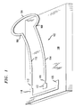
- FIG. 1 depicts a first inductor 102 in accordance with an illustrative embodiment of the present invention.
- Illustrative inductor 102 comprises conductive loop 104, conductive supports 110 and 114 incorporating passive self-assembly means, and three electrical contacts 118, 120 and 122, interrelated as shown.
- First end 106 of loop 104 depends from conductive support 110
- second end 108 of loop 104 depends from conductive support 114.
- Conductive supports 110 and 114 provide electrical connection to loop 104 and also function to physically separate loop 104 from substrate 100.
- first end 112 of conductive support 110 is electrically connected to ground contact 118.
- First end 116 of conductive support 114 is electrically connected to signal contact 122.
- a second ground contact 120 is electrically connected to contact 118.
- Ground contacts 118 and 120 are arranged in flanking relation to signal contact 122, providing the familiar ground-signal-ground arrangement. Such an arrangement provides guiding to a relatively high-frequency signal (e.g., greater than about 10 GHz) being delivered to signal contact 122.
- MCNC Microelectronics Center of North Carolina
- POLY0 The first deposited polysilicon layer
- POLY1 The upper two polysilicon layers
- POLY2 The upper two polysilicon layers
- POLY1 and/or POLY2 layers are released by etching away sacrificial oxide layers that are deposited between the polysilicon layers during fabrication.
- the polysilicon layers POLY0, POLY1 and POLY2 have nominal thicknesses of 0.5, 2, and 1.5 microns, respectively.
- the polysilicon and oxide layers are individually patterned, and unwanted material from each layer is removed by reactive ion etching before the next layer is added.
- a layer of metal nominally 0.6 - 1.3 microns in thickness, may be deposited on the POLY2 layer.
- MCNC's three-layer process, as well as other MEMS fabrication processes, are now quite familiar to those skilled in the art.
- FIGS. 2a - 2h An illustrative fabrication method for inductor 102 based on the aforedescribed MCNC three-layer process is described below and depicted in FIGS. 2a - 2h. For clarity of illustration, the fabrication of only one of the supports is shown. Certain layers of material that are deposited when using the MCNC process are not utilized when forming the present structure. To the extent that such unnecessary layers are deposited on the present structure during fabrication, they are completely removed in later lithographic steps. Such un-utilized layers are omitted for clarity of presentation. In the following description and the accompanying Figures, the MCNC designations for the various polysilicon layers will be used.
- a first layer POLY0 of polysilicon is deposited on an insulating layer IN, such as silicon nitride.
- the layer POLY0 is then patterned, using an appropriate mask.
- the as-patterned layer POLY0 p which will function as an "anchor" for a conductive support, is shown in FIG. 2b.
- a layer OX of oxide is deposited over the layer IN and the layer POLY0 p , as depicted in FIG. 2c.
- layer OX of oxide is patterned as shown in FIG. 2d.
- a layer POLY2 of polysilicon is deposited on the patterned layers OX p and POLYO p .
- the loop i.e., loop 104 shown in FIG. 1
- supports i.e., supports 110 and 114 shown in FIG. 1
- the layer POLY2 is patterned, using an appropriately-configured mask, into such structures.
- the patterned layer POLY2 p is depicted in FIG. 2f.
- a layer M of metal is deposited on layer POLY2 p , and then patterned.
- the metal is deposited over the supports, as well as the loop, and provides a conductive surface.
- FIG. 2g depicts the patterned layer M on the patterned layer POLY2 p .
- the layer OX of oxide is etched, such as with HF, releasing the patterned layer POLY2 p , as is depicted in FIG. 2h.
- two layers of metal are deposited everywhere on inductor 102 to reduce electrical resistance as compared to a single layer.
- three or more layers of metal are used to further reduce electrical resistance.
- Any one of a variety of metals may suitably be used for such purpose, including for example, aluminum, copper, silver or gold.
- gold is typically not used in conjunction with CMOS processes.
- the other metals listed above should be used in preference to gold.
- patterned layer POLY2 p As patterned layer POLY2 p is released, it warps, such that the non-anchored end (where the inductor loop is) moves upwardly away from the layer IN disposed on the substrate. Such upward warping results from incorporating the aforementioned passive self-assembly means.
- passive self-assembly means comprises a layer of material that is deposited to have a high level of intrinsic stress ("stressed layer").
- the stressed layer is deposited over the structural layer (e.g., the polysilicon) of the structure that is to be warped.
- the stressed layer is deposited on top of the patterned layer POLY2 p , as is described in more detail below.
- metal was deposited on the POLY2 layer to provide a conductive surface. That metal is typically gold (for non-CMOS applications). Gold does not, however, adhere well to polysilicon. As such, a thin adhesion layer is often deposited on the POLY2 layer before depositing gold.
- the material serving as an adhesion layer is, advantageously, the passive self-assembly means.
- chromium is advantageously used as the adhesion layer/passive self-assembly means. A high intrinsic stress is associated with the deposited chromium layer. When the sacrificial oxide layer is etched away to release the patterned layer POLY2 p , the chromium layer contracts to minimize strain.
- patterned layer POLY2 p is fabricated with compressive stress, and an overlying layer (e.g., metal) is deposited with low stress. Upon release. the POLY2 p layer expands, causing the same upwardly-directed warp.
- an overlying layer e.g., metal
- the POLY1 layer of the MCNC process is not used; rather the POLY2 layer is used.
- the POLY2 layer is thinner than the POLY1 layer (2 microns).
- the POLY2 will be more amenable to "warping," as is desired for raising the supports 110 and 114 and loop 104 up and away from the substrate.
- metal is advantageously deposited on the structural (e.g., polysilicon) layer comprising those structures. In the MCNC process, metal cannot be deposited on the POLY1 layer, but can be deposited on the POLY2 layer.
- inductor 102 can be fabricated using other surface micromachining processes.
- FIG. 3 depicts a second inductor 202 in accordance with an illustrative embodiment of the present invention.
- Illustrative inductor 202 comprises conductive spiral 204 including passive self-assembly means, and four electrical contacts or pads 218, 220, 222 and 224, interrelated as shown.
- First end 206 of spiral 204 is electrically connected to signal contact 222 and second end 208 of spiral 204 is electrically connected to return contact 224.
- a conductive substrate is used as a return to grounds 218 and 220.
- First and second ground contacts 218 and 220 are electrically connected to one another and arranged in flanking relation to signal contact 222, providing a ground-signal-ground arrangement.
- Pads 218 - 224 are deposited on an underlying electrically insulating layer (not shown) disposed on substrate 200, such that pads 222 and 224 anchoring inductor 202.
- a portion of spiral 204 aligned with diameter A-A rests on, but is not anchored to, underlying substrate 200.
- the spiral 204 is "folded" along diameter A-A, dividing the spiral into two portions, each of which portions curve upwardly away from substrate 200.
- Inductor 202 can be fabricated applying the aforedescribed surface micromaching methods, adapted as required for differences in structure.
- the passive self-assembly means comprises a stressed layer, such as is described in conjunction with the previous embodiment.
- the stressed layer is deposited over the structural layer (e.g., polysilicon) of spiral 204.
- the structural layer e.g., polysilicon
- dimples are advantageously patterned in layer OX (i.e., the OXIDE1 layer of the MCNC 3-layer process) along axis A-A. Such dimples, which are repeated in the POLY2 layer forming the inductor spiral, weaken the spiral, facilitating folding along axis A-A as the spiral warps.
- inductor 202 is anchored to the underlying layer (i.e., an insulating layer disposed on top of the substrate) at the pads 222 and 224 along the axis A-A, spiral 204 warps upwardly on either side of axis A-A, forming the familiar "taco" shape.
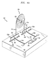
- inductor 102/202 There will be some degree of interaction (e.g., electrical losses, inductive coupling, parasitic capacitances) between inductor 102/202 and its respective substrate due to the proximity and relative orientation of the loop/spiral element to such substrate. Such interaction is reduced to essentially negligible levels in an inductor 302 in accordance with an illustrative embodiment of the present invention. Inductor 302 is depicted in FIG. 4a.
- Spiral 304 of inductor 302 is disposed in orthogonal relation to substrate 300.
- Conductive supports 310 and 314 support spiral 304 in an upright, out-of-the-plane-of-the-substrate orientation.
- Conductive supports 310 and 314 are attached to respective conductive hinged plates 332a and 332b.
- the hinged plates are rotatably attached to substrate 300 by hinges 338.
- the formation of such hinged plates is known in the art. See, for example, Pister et al., "Microfabricated Hinges,” v. 33, Sensors and Actuators A, pp. 249-256, 1992. See also, assignee's co-pending U.S. Pat.
- Hinged plates 332a/332b have a v-shaped notch 334 that receives a v-shaped engagment member 342 that depends from a first end of conductive passive actuating elements 340a and 340b.
- passive self-assembly means comprises the aforementioned v-shaped notch 334, v-shaped engagement member 342 and passive actuating elements 340a and 340b.
- Contacts 350, 352 and 354 arranged in the well-known ground-signal-ground arrangement, provide electrical connection to spiral 304 through the passive actuating elements, hinged plates and conductive supports. Segment 305 depending from the inner end of spiral 304 provides a return path through support 314, hinged plate 332b and passive actuating element 340b to ground contacts 350 and 354.
- spiral 304, conductive supports 310/314, hinged plates 332a/332b and passive actuating elements 340a/340b lie flat on the surface of substrate 300 (or on an insulating layer disposed on the substrate).
- a portion of v-shaped engagment member 342 of actuating element 340a lies beneath v-shaped notch 334 of hinged plate 332a.
- a portion of v-shaped engagment member 342 of actuating element 340b lies beneath v-shaped notch 334 of hinged plate 332b.
- Passive actuating elements 340a and 340b comprise a stressed layer that can be implemented in the manner previously described.
- the stressed layer contracts to minimize strain, causing passive actuating elements 340a/340b to rise up and away from substrate 300.
- a maximum displacement between substrate 300 and the passive actuating elements occurs at the first end wherein the v-shaped engagment member 342 is disposed and a minimum (no displacement) occurs at a second end wherein the passive actuating elements 340a/340b are anchored to the substrate (or to overlying layers).
- FIGS. 4b and 4c depict the passive assembly process for the illustrative inductor depicted in FIG. 4a.
- FIGS. 4b and 4c show only a single hinged plate and passive actuating element for clarity of presentation.
- FIG. 4b depicts hinged plate 332a and passive actuating element 340a lying on substrate 300.
- edges 436a/436b of v-shaped notch 334 in hinged plate 332a slide over edges 444a/444b of v-shaped engagement member 342.
- hinged plate 332a is rotated up and away from substrate 300 about its hinges 338.
- vertex 343 of v-shaped engagment member 342 and vertex 335 of v-shaped notch 334 converge to a final position, depicted in FIG. 4c.
- hinged plate 332a In the final position, hinged plate 332a is substantially orthogonal to substrate 300, having been rotated about ninety degrees out-of-plane about hinges 338. Stop 344 prevents hinged plate 332a from “flipping-over” and falling towards substrate 300 on top of passive actuating element 340a. See the present assignee's copending patent application entitled “Self-Assembling Micro-Mechanical Device,” filed December 22, 1997 as U.S. Pat. App. Ser. No. 08/997,175, incorporated herein by reference.
- inductors such as illustrative inductors 102, 202 and 302
- loop 104 comprises a single (or more properly, a partial) turn.
- the loop can comprise additional turns to provide more inductance.
- spiral 204 comprises three turns. It should be understood that the three illustrative inductors 102, 202 and 302 can be fabricated as a loop ( i.e., a partial turn to a full turn) or a spiral (more than one turn).
- a spiral inductor has a greater inductance than a loop ( i.e., single turn) inductor.
- a spiral inductor disadvantageously requires a return path underneath the multiple turns. Such a return path is provided by a conductive substrate in the embodiment depicted in FIG. 2, and by segment 305 in the embodiment depicted in FIG. 4a. The aforedescribed disadvantage is avoided in a fourth and fifth embodiment of the present inductor, depicted in plan views FIGS. 5a and 5b, respectively.
- FIG. 5a depicts a plan view of inductor 402.
- Inductor 402 comprises meander line 404, conductive supports 410 and 414 incorporating passive self-assembly means, and three electrical contacts 418, 420 and 422, interrelated as shown.
- First end 406 of meander line 404 depends from conductive support 410
- second end 408 of meander line 404 depends from conductive support 414.
- Conductive supports 410 and 414 provide electrical connection to meander line 404 and also function to physically separate the meander line from an underlying substrate 400.
- Conductive support 410 is anchored, and electrically connected, to ground contact 418.
- Ground contact 418 is electrically connected to ground contact 420 providing a ground-signal-ground arrangement.
- Conductive support 414 is anchored, and electrically connected, to signal contact 422.
- FIG. 5b depicts inductor 502.
- Inductor 502 comprises dual loops 504a and 504b, conductive supports 510a, 510b and 514 incorporating passive self-assembly means, and three electrical contacts 518, 520 and 522, interrelated as shown.
- First end 506a of loop 504a depends from conductive support 510a
- first end 506b of loop 504b depends from conductive support 510b.
- Second end 508a of loop 504a and second end 508b of loop 504b depend from conductive support 514.
- Conductive support 510a is anchored, and electrically connected, to ground contact 518.
- Conductive support 510b is anchored, and electrically connected, to ground contact 520.
- conductive support 514 is anchored, and electrically connected, to signal contact 522.
- the convolutions of meander line 404 increase the inductance of inductor 402 relative to an inductor having an non-convoluted loop, such as illustrative inductor 102 depicted in FIG. 1.
- the interacting fields of loops 504a and 504b increase the inductance of inductor 502 relative to the solitary loop of illustrative inductor 102 depicted in FIG. 1.
- illustrative inductors 402 and 502 advantageously possess the higher inductance of a "spiral" inductor, yet do not require a return path.
- loop is intended to encompass an inductor element configured as a loop (partial or single turn), spiral (multiple turns), meander line and dual loops, as those terms are defined/described above.
- the present inductor can advantageously be monolithically integrated into a number of important circuits using commercial-scale processing, thereby providing a commercially-viable method for providing a single-chip version of such circuits.
- Illustrative applications include many very basic circuits, including for example, reactive impedance matching circuits, tank circuits, and filters.
- the present inductor can also be incorporated into more complex devices, such as variable-frequency oscillators (VFOs) and transceivers, that utilize such circuits.
- VFOs variable-frequency oscillators
- BiMOSIIe® One such process is the "BiMOSIIe®” process available from Analog Devices, Inc. of Norwood, Massachusetts.
- the BiMOSIIe® process integrates a surface micromachining process suitable for forming MEMS structures with a CMOS process suitable for forming devices useful for analog applications.
- the BiMOSIIe® process nominally utilizes a single structural polysilicon layer and associated sacrificial layer (to release the structural polysilicon layer). Additional polysilicon layers can be used in this or other processes to provide more functionality as desired.
- Information concerning the BiMOSIIe® process is provided on Analog Devices/ MCNC server pages at http://imems.mcnc.org. See also, U.S. Pat. No.
- FIG. 6a depicts a portion of a circuit 600a including a typical implementation of a transistor T1 on a substrate.
- First capacitor C1 and second capacitor C2 are representative of parasitic capacitances that are generated by virtue of the circuitry required to implement transistor T1 on a substrate.
- a portion of RF signal S RF is lost to such parasitic capacitances, as represented by signal loss SL 1 and SL 2 .
- signal loss can be substantially reduced by incorporating impedance-matching elements into circuit 600a.
- FIG. 6b depicts a modification in accordance with the present teachings of the circuit shown in FIG. 6a, wherein the present MEMS-implemented inductors are added to provide reactive impedance matching.
- Impedance-matched circuit 600b incorporates passive self-assembling inductors L1 and L2, which are fabricated and configured in accordance with the present teachings. Parasitic capacitances C1 and C2 are substantially canceled by virtue of the inductive reactance of inductors L1 and L2. As a result, improvements in power transfer and circuit noise performance are realized.
- the present inductor is used to form an improved LC circuit, sometimes referred to as a "tank" circuit.
- a LC circuit consists of an inductor and a capacitor, connected either in series or in parallel. It is a property of a LC circuit, whether a series or a parallel circuit, that when the impedance Z L (or reactance X L ) of the inductor and the impedance Z c (reactance X C ) of the capacitor are equal, the circuit is in resonance.
- LC circuits extremely useful and important.
- Series and parallel resonant LC circuits are advantageously used, for example, as radio frequency and power supply filters, in intermediate frequency transformers of radio and television receivers, in drive and power stages of transmitters, as well in the oscillator stages of transmitters, receivers and frequency-measuring equipment.
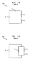
- FIG. 7a depicts a conventional series LC circuit 750S
- FIG. 7b depicts a conventional parallel LC circuit 750P
- Circuit 750S includes signal source G3, capacitor C3, inductor L3 and resistor R3, connected in series as shown.
- Circuit 750P includes the same elements ( i.e., signal source G4, capacitor C4, inductor L4 and resistor R4), but connected in a parallel configuration.
- Resistors R3 and R4 are not actual circuit elements, but are included to account for the inherent resistance of the circuit components, particularly the inductor.
- the LC circuits of FIGS. 7a and 7b can be implemented as either fixed LC circuits or variable LC circuits.
- fixed LC circuits there is no ability to vary the inductance of the inductor or the capacitance of the capacitor.
- Such fixed circuits therefore have a fixed resonance.
- a variable LC circuit having an adjustable resonance frequency can be implemented using a fixed inductor and a variable capacitor.
- a monolithically-integrable, CMOS-compatible, fixed LC circuit in accordance with an illustrative embodiment of the present invention includes a MEMS-based fixed inductor, such as illustrative inductors 102, 202 or 302 and a capacitor, such as an oxide capacitor, or a micro-machined capacitor, both known in the art.
- a monolithically-integrable, CMOS-compatible, variable LC circuit in accordance with an illustrative embodiment of the present invention includes a MEMS-based fixed inductor and a variable capacitor or varactor, such as a diode varactor well known in the art, or a MEMS-based variable capacitor such as is described in applicants' co-pending U.S. patent application serial no.: , filed , and entitled "Article Comprising A Multi-Port Variable Capacitor," attorney docket: Barber 8-25-11-1, incorporated by reference herein.
- FIG. 8a depicts an illustrative notch filter NF in accordance with an illustrative embodiment of the present invention.
- Notch filter NF includes shunt resonator (LC circuit) LC1 that shunts signal line S1 to ground G.
- Shunt resonator LC1 includes a passive self-assembling inductor L5 in accordance with the present teachings, and a capacitor C5.
- Notch filter NF suppresses signal transmission at the resonant frequency of resonator LC1, and passes substantially all other frequencies.
- FIG. 8b depicts a pass filter PF in accordance with an illustrative embodiment of the present invention.
- Pass filter RF includes series resonator (LC circuit) LC2.
- Series LC2 includes a passive self-assembling inductor L6 in accordance with the present teachings, and a capacitor C6.
- Pass filter PF passes a signal at the resonant frequency of resonator LC2, and suppresses substantially all other frequencies.
- FIG. 8c depicts band pass filter BPF in accordance with an illustrative embodiment of the present invention.
- Band pass filter BPF includes two series resonators LC3 and LC4 and shunt resonator LC5, interrelated as shown.
- Resonators LC3, LC4 and LC5 include respective passive self-assembling inductor L7, L8 and L9, as well as respective capacitors C7, C8 and C9.
- the values of inductors L7, L8 and L9, and capacitors C7, C8 and C9 are suitably selected such that filter BPF will pass signals having a frequency within a desired band or range, and "stop" signals having frequencies outside of the band.
- the capacitors used in the resonators LC1 - LC5 can be fixed or variable. If variable capacitors are used, then the frequency characteristics of the resonators, and hence the filters, can be changed by an applied control voltage.
- Such a tunable filter is particularly advantageous for use in an equalizer for high frequency amplifiers.
- Such an equalizer can be used in a feedback configuration to tailor the spectrum of the amplifier to a desired function. It should be appreciated that a wide variety of other arrangements incorporating the present inductor may suitably be used to provide a filtering function.
- LC circuits are important elements of more complicated devices, including, for example, VFOs.
- the CMOS compatible, monolithically-integrable LC circuits previously described can be used to form a monolithically-integrable VFO.
- generic layouts suitable for use in conjunction with the present invention are described below. In application of the guidelines provided herein and well understood principles of oscillator design, those skilled in the art will be able to configure VFOs in accordance with the present teachings in a wide variety of ways as suits a particular application.
- the present VFOs are radio-frequency oscillators.
- An oscillator is a device or circuit that converts DC power to RF power.
- the present solid-state oscillators incorporate a nonlinear active device, such as a diode or transistor, which is biased so as to be in an unstable, "negative-resistance" regime.
- the phrase "negative resistance” is used to describe a process whereby energy is coupled into the resonant structure in a manner that allows the resonant structure to sustain rf oscillations, and is a requirement for producing net RF power.
- Oscillation frequency of the oscillator is determined by load and terminating circuits, as well as by a frequency-selective network, often implemented as a resonant structure which, in the present invention, includes the present MEMS-based inductor.
- Capacitance can be obtained from a capacitor in an LC circuit proper that includes the MEMS-based inductor, or from other structures (e.g. , capacitors within an amplification device) included in the oscillator.
- most embodiments of the present MEMS-based inductor have a capacitance associated therewith, which, in conjunction with other capacitive structures in the oscillator, provides for suitable operation of the resonant structure.
- VFO variable frequency oscillator
- an improved VFO in accordance with the present teachings utilizes the present inductor in the well known configuration of a one-port negative-resistance oscillator.
- a one-port negative-resistance oscillator is conceptually depicted in FIG. 9.
- Such an oscillator can be conceptualized as including a load L and a negative-resistance input device IN.
- the negative resistance device is a Gunn or IMPATT diode, which is biased to create a negative resistance.
- the load comprises a resonant structure, such as an LC circuit including the present passive self-assembling inductor.
- oscillator design requires consideration of factors other than those described above, such as, for example, selection of an operating point for stable operation and maximum power output, frequency pulling, large signal effects and noise characteristics. Such factors are well understood by those skilled in the art, and will not be described herein.
- FIG. 11 depicts a conventional amplifier-based VFO.
- Such an oscillator includes a frequency-dependent or resonant structure RS and an amplification device A.
- the power output port can be on either side of amplification device A, which is commonly implemented as a transistor.
- the resonant structure comprises an LC circuit including the present passive self-assembling inductor.
- the amplifier is implemented such that it is operable, at an input, to monitor the rf signal in the resonant structure, and further operable, at an output, to inject an amplified signal into the resonant structure in a manner best suited to sustain oscillations in the resonant structure.
- amplification device suitable for providing the above-described functions.
- the configuration of the transistor in the oscillator depends, in large part, on the specifics of transistor.
- transistors common source or common gate configurations are typically used.
- bipolar transistors common emitter and common base configurations are more typical.
- Two well-known configurations of a transistor-based negative-resistance one-port oscillator include the Colpitts oscillator, depicted in a very basic embodiment in FIG. 12, and the Clapp oscillator, depicted in a very basic embodiment in FIG. 13. Both oscillators are shown utilizing bipolar transistors as their amplification element in a common-base configuration.
- the Colpitts oscillator comprises two variable capacitors VC1 and VC2, transistor T2 and inductor L5, electrically connected as shown. While both capacitors are shown as variable capacitors, in other embodiments of a Colpitts oscillator, VC2 is replaced by a fixed capacitor.
- the Clapp oscillator comprises two fixed capacitors C5 and C6, variable capacitor VC3, inductor L6 and transistor T3, electrically connected as shown. Improved versions of the basic Colpitts and Clapp oscillators incorporate the passive self-assembling inductors described herein.
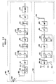
- FIG. 15 depicts a simplified block diagram of a conventional transceiver 800.
- Transceiver 800 includes receiver 802 and transmitter 840.
- Illustrative receiver 802 consists of antenna 806, RF band-pass filter 808, amplifier 812, first downconverter 816, first intermediate-frequency band-pass filter 822, first intermediate-frequency amplifier 826, second downconverter 828, second intermediate-frequency band-pass filter 834, second intermediate-frequency amplifier 836 and demodulator 838, interrelated as shown.
- Receiver 802 operates as follows.
- Signal 804 comprising a plurality of modulated RF carrier signals having different frequencies within a first frequency band
- antenna 806 receives a plurality of undesired signals covering an extremely wide range of frequencies outside the first frequency band.
- Signal 804 and the undesired signals are routed to RF band-pass filter 808, which delivers an output signal 810 comprising substantially only those signals having frequencies within the first frequency band.
- Signal 810 is amplified in low-noise amplifier 812, which generates amplified signal 814.
- Signal 814 is fed to first downconverter 816.
- First downconverter 816 consists of local oscillator 818, and a mixer 820.
- first intermediate-frequency band-pass filter 822 After downconversion, the signal passes to first intermediate-frequency band-pass filter 822. Filter 822 typically provides extreme attenuation outside its pass band. The filtered signal is then delivered to first intermediate-frequency amplifier 826. Since illustrative receiver 802 is implemented in the well known double superheterodyne arrangement, it includes second downconverter 828, which receives the amplified signal from amplifier 826. Second downconverter 828 generates a second intermediate frequency signal having a somewhat lower frequency than that generated by first downconverter 816. The downconverted signal from second downconverter 828 passes to second intermediate-frequency band-pass filter 834 and then to second intermediate-frequency amplifier 836.
- second downconverter 828 comprises local oscillator 830 and mixer 832.
- the signal from second intermediate-frequency amplifier 836 is passed to demodulator 838 for information retrieval.
- the second down conversion may be omitted.
- Illustrative transmitter 840 includes modulator 844, local oscillator 846, upconverter 852, band-pass filter 858, upconverter 860, band-pass filter 866, amplifier 868 and antenna 870, interrelated as shown.
- Message 842 is modulated, via modulator 844, on to a carrier signal 848 generated by local oscillator 846.
- Modulated output signal 850 is shifted, via upconverter 852, to an intermediate frequency (IF) that is at least twice the highest output frequency of said signal 850.
- Upconverter 852 consists of local oscillator 854 and mixer 856.
- the IF signal leaving mixer 856 is filtered in band-pass filter 858 and then up converted to the desired output frequency by upconverter 860.
- Upconverter 860 includes local oscillator 862 and mixer 864.
- the up converted signal leaving mixer 864 is filtered in filter 866 and then amplified, in amplifier 868, to the desired power level.
- the amplified signal is then delivered to antenna 870 for transmission.
- FIG. 16 depicts an illustrative circuitboard-level implementation 900 of receiver 802 of transceiver 800.
- RF band-pass filter 808, first intermediate-frequency band-pass filter 822, and second intermediate-frequency band-pass filter 834 are implemented on three different chips on circuit board 902.
- filter 808, a ceramic-based device resides on chip 904
- filter 822, a surface acoustic wave-based device resides on chip 910
- filter 834, a crystal-based device resides on chip 912.
- Local oscillators 818 and 830 are implemented on chip 908, while the transistor-based electronics, implemented as CMOS, reside on chip 906.
- a transceiver is implemented on as few as a single CMOS chip by monolithically integrating the various filters and oscillators with the transistor electronics.
- MEMS-based filters or other thin-film resonators suitable for use in conjunction with an improved transceiver in accordance with the present teachings can be designed and fabricated according to the teachings of U.S. Pat. No. 09/009599, filed January 20, 1998 entitled "Article Comprising a Micromachined Filter,” incorporated by reference herein.
- other MEMS-based filters, and methods for making such filters are known to those skilled in the art. Such filters may suitably be used for making the present transceiver.
- Monolithic incorporation of such oscillators is facilitated by incorporating the present MEMS-based LC circuits described above into such oscillators. Note that antennas are located off-chip.
Landscapes
- Engineering & Computer Science (AREA)
- Chemical & Material Sciences (AREA)
- Nanotechnology (AREA)
- Crystallography & Structural Chemistry (AREA)
- Physics & Mathematics (AREA)
- Condensed Matter Physics & Semiconductors (AREA)
- Materials Engineering (AREA)
- General Physics & Mathematics (AREA)
- Composite Materials (AREA)
- Manufacturing & Machinery (AREA)
- Microelectronics & Electronic Packaging (AREA)
- Mathematical Physics (AREA)
- Theoretical Computer Science (AREA)
- Inductance-Capacitance Distribution Constants And Capacitance-Resistance Oscillators (AREA)
- Semiconductor Integrated Circuits (AREA)
- Coils Or Transformers For Communication (AREA)
- Filters And Equalizers (AREA)
- Micromachines (AREA)
Applications Claiming Priority (2)
| Application Number | Priority Date | Filing Date | Title |
|---|---|---|---|
| US152189 | 1980-05-22 | ||
| US09/152,189 US6101371A (en) | 1998-09-12 | 1998-09-12 | Article comprising an inductor |
Publications (2)
| Publication Number | Publication Date |
|---|---|
| EP0986106A1 true EP0986106A1 (fr) | 2000-03-15 |
| EP0986106B1 EP0986106B1 (fr) | 2007-10-03 |
Family
ID=22541875
Family Applications (1)
| Application Number | Title | Priority Date | Filing Date |
|---|---|---|---|
| EP99306918A Expired - Lifetime EP0986106B1 (fr) | 1998-09-12 | 1999-08-31 | Dispositif comprenant un composant inductif |
Country Status (4)
| Country | Link |
|---|---|
| US (1) | US6101371A (fr) |
| EP (1) | EP0986106B1 (fr) |
| JP (2) | JP2000150251A (fr) |
| DE (1) | DE69937217T2 (fr) |
Cited By (16)
| Publication number | Priority date | Publication date | Assignee | Title |
|---|---|---|---|---|
| EP1231617A1 (fr) * | 2001-02-09 | 2002-08-14 | Xerox Corporation | Structures de micro-dispositif hors plan |
| EP1231616A1 (fr) * | 2001-02-09 | 2002-08-14 | Xerox Corporation | Structures de micro-dispositif hors plan |
| US6438954B1 (en) | 2001-04-27 | 2002-08-27 | 3M Innovative Properties Company | Multi-directional thermal actuator |
| US6483419B1 (en) | 2000-09-12 | 2002-11-19 | 3M Innovative Properties Company | Combination horizontal and vertical thermal actuator |
| US6531947B1 (en) | 2000-09-12 | 2003-03-11 | 3M Innovative Properties Company | Direct acting vertical thermal actuator with controlled bending |
| WO2003048032A1 (fr) * | 2001-12-04 | 2003-06-12 | Max-Planck Gesellschaft Zur Förderung Der Wissenschaft E.V. | Realisation de bobines, de transformateurs et de condensateurs microscopiques et nanoscopiques par enroulement ou repliement de couches conductrices au cours du decollement de couches auxiliaires d'un substrat |
| US6708491B1 (en) | 2000-09-12 | 2004-03-23 | 3M Innovative Properties Company | Direct acting vertical thermal actuator |
| EP1209725A3 (fr) * | 2000-11-27 | 2006-01-11 | Megic Corporation | Système à haute performance sur un chip utilisant un procédé après une étape de passivation |
| DE102005030384B3 (de) * | 2005-06-29 | 2006-11-02 | Siemens Ag | Antennevorrichtung für Funk basierte Telefone |
| EP1309976A4 (fr) * | 2000-06-09 | 2007-08-15 | Xerox Corp | Structures de bobinages hors du plan configurees de maniere photolithographique |
| EP1389340A4 (fr) * | 2001-05-23 | 2009-08-05 | Univ Illinois | Inducteur sureleve sur la puce et procede de fabrication de l'inducteur |
| US8384508B2 (en) | 2001-09-04 | 2013-02-26 | Megica Corporation | Method for making high-performance RF integrated circuits |
| US8384189B2 (en) | 2005-03-29 | 2013-02-26 | Megica Corporation | High performance system-on-chip using post passivation process |
| US8742580B2 (en) | 2002-10-15 | 2014-06-03 | Megit Acquisition Corp. | Method of wire bonding over active area of a semiconductor circuit |
| US8749021B2 (en) | 2006-12-26 | 2014-06-10 | Megit Acquisition Corp. | Voltage regulator integrated with semiconductor chip |
| US8809951B2 (en) | 2008-12-26 | 2014-08-19 | Megit Acquisition Corp. | Chip packages having dual DMOS devices with power management integrated circuits |
Families Citing this family (44)
| Publication number | Priority date | Publication date | Assignee | Title |
|---|---|---|---|---|
| DE69920273T2 (de) * | 1998-11-12 | 2005-09-22 | Broadcom Corp., Irvine | Integrierte tunerarchitektur |
| US8178435B2 (en) | 1998-12-21 | 2012-05-15 | Megica Corporation | High performance system-on-chip inductor using post passivation process |
| US8421158B2 (en) | 1998-12-21 | 2013-04-16 | Megica Corporation | Chip structure with a passive device and method for forming the same |
| JP2000278042A (ja) * | 1999-03-26 | 2000-10-06 | Sony Corp | 発振回路及びチューナ |
| US6850353B1 (en) | 1999-06-11 | 2005-02-01 | University Of Hawaii | MEMS optical components |
| US6859299B1 (en) | 1999-06-11 | 2005-02-22 | Jung-Chih Chiao | MEMS optical components |
| AU5480500A (en) * | 1999-06-11 | 2001-01-02 | University Of Hawaii | Mems optical components |
| US7151298B1 (en) * | 1999-12-20 | 2006-12-19 | Advanced Micro Devices, Inc. | Electrostatic discharge protection network having distributed components |
| JP2001274528A (ja) | 2000-01-21 | 2001-10-05 | Fujitsu Ltd | 薄膜デバイスの基板間転写方法 |
| US6683508B1 (en) | 2000-09-22 | 2004-01-27 | Agere Systems, Inc. | System and method of increasing a self-resonant frequency of a tuning circuit and an oscillator employing the same |
| US6706202B1 (en) * | 2000-09-28 | 2004-03-16 | Xerox Corporation | Method for shaped optical MEMS components with stressed thin films |
| AU2002225777A1 (en) * | 2000-11-28 | 2002-06-11 | Fraunhofer Usa, Inc. | Method of manufacturing ultra-precise, self-assembled micro systems |
| WO2002049050A1 (fr) * | 2000-12-11 | 2002-06-20 | Koninklijke Philips Electronics N.V. | Bobine de bande |
| US6824521B2 (en) * | 2001-01-22 | 2004-11-30 | Integrated Sensing Systems, Inc. | Sensing catheter system and method of fabrication |
| US6543087B2 (en) | 2001-06-01 | 2003-04-08 | Aip Networks, Inc. | Micro-electromechanical hinged flap structure |
| US6781239B1 (en) * | 2001-12-05 | 2004-08-24 | National Semiconductor Corporation | Integrated circuit and method of forming the integrated circuit having a die with high Q inductors and capacitors attached to a die with a circuit as a flip chip |
| US7011530B2 (en) * | 2002-05-24 | 2006-03-14 | Sitaraman Suresh K | Multi-axis compliance spring |
| EP1540839A4 (fr) * | 2002-08-20 | 2008-01-02 | Lockheed Corp | Procede et dispositif permettant de modifier une reponse en radiofrequence |
| US6856499B2 (en) | 2003-03-28 | 2005-02-15 | Northrop Gurmman Corporation | MEMS variable inductor and capacitor |
| US6862441B2 (en) | 2003-06-09 | 2005-03-01 | Nokia Corporation | Transmitter filter arrangement for multiband mobile phone |
| JP2005057270A (ja) * | 2003-08-01 | 2005-03-03 | Stmicroelectronics Sa | 切換え可能なインダクタンス |
| US7950134B2 (en) * | 2003-12-08 | 2011-05-31 | Cochlear Limited | Implantable antenna |
| WO2009065127A1 (fr) | 2007-11-16 | 2009-05-22 | Cochlear Americas | Rangée d'électrodes et procédé de formation d'une rangée d'électrodes |
| US7262680B2 (en) * | 2004-02-27 | 2007-08-28 | Illinois Institute Of Technology | Compact inductor with stacked via magnetic cores for integrated circuits |
| KR20080002933A (ko) * | 2005-04-08 | 2008-01-04 | 엔엑스피 비 브이 | 전기발진신호 발생 전자 장치 및 방법 |
| CN1901162B (zh) | 2005-07-22 | 2011-04-20 | 米辑电子股份有限公司 | 连续电镀制作线路组件的方法及线路组件结构 |
| US7410894B2 (en) * | 2005-07-27 | 2008-08-12 | International Business Machines Corporation | Post last wiring level inductor using patterned plate process |
| KR100620812B1 (ko) * | 2005-08-08 | 2006-09-07 | 삼성전자주식회사 | 웨이퍼 레벨 재배선으로 형성된 터미네이션 회로선을 갖는반도체 소자 |
| JP4893112B2 (ja) * | 2006-06-03 | 2012-03-07 | 株式会社ニコン | 高周波回路コンポーネント |
| US20080001700A1 (en) * | 2006-06-30 | 2008-01-03 | Flavio Pardo | High inductance, out-of-plane inductors |
| US20080027311A1 (en) * | 2006-07-14 | 2008-01-31 | General Electric Company | Resonant transponder using self-resonance of coil |
| US7839242B1 (en) | 2006-08-23 | 2010-11-23 | National Semiconductor Corporation | Magnetic MEMS switching regulator |
| US20080102906A1 (en) * | 2006-10-30 | 2008-05-01 | Phonak Ag | Communication system and method of operating the same |
| US7710232B1 (en) * | 2007-05-09 | 2010-05-04 | Sandia Corporation | Microelectromechanical tunable inductor |
| US8672667B2 (en) * | 2007-07-17 | 2014-03-18 | Cochlear Limited | Electrically insulative structure having holes for feedthroughs |
| US7936240B2 (en) * | 2007-08-16 | 2011-05-03 | Simon Fraser University | Lithographically controlled curvature for MEMS devices and antennas |
| FR2937422B1 (fr) * | 2008-10-22 | 2010-12-10 | Total Raffinage Marketing | Dispositif pour le controle de la qualite d'un lubrifiant et procede pour le controle du fonctionnement d'un equipement industriel utilisant un lubrifiant |
| WO2010052839A1 (fr) * | 2008-11-06 | 2010-05-14 | パナソニック株式会社 | Dispositif à semi-conducteur |
| JP2011130083A (ja) * | 2009-12-16 | 2011-06-30 | Mitsubishi Electric Corp | 可変フィルタ |
| US8373543B2 (en) * | 2009-12-22 | 2013-02-12 | Bae Systems Information And Electronic Systems Integrations Inc. | RFID transponder using ambient radiation |
| US8907447B2 (en) | 2010-02-19 | 2014-12-09 | Mingliang Wang | Power inductors in silicon |
| JP2013074496A (ja) * | 2011-09-28 | 2013-04-22 | Onkyo Corp | 分波回路 |
| US8909188B2 (en) * | 2012-10-31 | 2014-12-09 | Cambridge Silicon Radio, Ltd. | Mixer |
| JP6278925B2 (ja) * | 2015-04-24 | 2018-02-14 | 三菱電機株式会社 | マルチポートスイッチ |
Citations (3)
| Publication number | Priority date | Publication date | Assignee | Title |
|---|---|---|---|---|
| WO1994017558A1 (fr) * | 1993-01-29 | 1994-08-04 | The Regents Of The University Of California | Composant monolithique passif |
| WO1996028841A1 (fr) * | 1995-03-10 | 1996-09-19 | Elisabeth Smela | Procede pour fabriquer des structures microusinees et structures obtenues par ce procede |
| US5635750A (en) * | 1994-10-18 | 1997-06-03 | Siemens Aktiengesellschaft | Micromechanical relay with transverse slots |
Family Cites Families (10)
| Publication number | Priority date | Publication date | Assignee | Title |
|---|---|---|---|---|
| US3932824A (en) * | 1970-03-06 | 1976-01-13 | Wycoff Keith H | Signal selective circuit |
| US3697911A (en) * | 1971-01-20 | 1972-10-10 | William A Strauss Jr | Coil form |
| JPS5612819Y2 (fr) * | 1976-02-26 | 1981-03-25 | ||
| US4733190A (en) * | 1987-03-16 | 1988-03-22 | Medical Advances, Inc. | NMR local coil with adjustable spacing |
| JPH05159938A (ja) * | 1991-12-02 | 1993-06-25 | Murata Mfg Co Ltd | インダクタンス可変コイル |
| US5437057A (en) * | 1992-12-03 | 1995-07-25 | Xerox Corporation | Wireless communications using near field coupling |
| DE4418432A1 (de) * | 1994-05-26 | 1995-11-30 | Siemens Ag | Frequenzveränderbare Oszillatoranordnung |
| JPH08222694A (ja) * | 1995-02-13 | 1996-08-30 | Toshiba Corp | 半導体装置および半導体装置の製造方法 |
| JP3378435B2 (ja) * | 1995-09-29 | 2003-02-17 | 株式会社東芝 | 超高周波帯無線通信装置 |
| CA2212504C (fr) * | 1996-08-09 | 2004-11-16 | Mesta Electronics, Inc. | Filtre d'harmonique actif et correcteur du facteur de puissance |
-
1998
- 1998-09-12 US US09/152,189 patent/US6101371A/en not_active Expired - Lifetime
-
1999
- 1999-08-31 EP EP99306918A patent/EP0986106B1/fr not_active Expired - Lifetime
- 1999-08-31 DE DE69937217T patent/DE69937217T2/de not_active Expired - Lifetime
- 1999-09-09 JP JP11255686A patent/JP2000150251A/ja not_active Withdrawn
-
2007
- 2007-03-09 JP JP2007060148A patent/JP4880501B2/ja not_active Expired - Fee Related
Patent Citations (3)
| Publication number | Priority date | Publication date | Assignee | Title |
|---|---|---|---|---|
| WO1994017558A1 (fr) * | 1993-01-29 | 1994-08-04 | The Regents Of The University Of California | Composant monolithique passif |
| US5635750A (en) * | 1994-10-18 | 1997-06-03 | Siemens Aktiengesellschaft | Micromechanical relay with transverse slots |
| WO1996028841A1 (fr) * | 1995-03-10 | 1996-09-19 | Elisabeth Smela | Procede pour fabriquer des structures microusinees et structures obtenues par ce procede |
Non-Patent Citations (2)
| Title |
|---|
| ALLAN R: "MEMS TECHNOLOGY PURSUED FOR THE DEVELOPMENT OF MICROMACHINED SILICON VARIABLE INDUCTORS AND LATCHING ACCELEROMETERS", ELECTRONIC DESIGN,US,PENTON PUBLISHING, CLEVELAND, OH, vol. 45, no. 13, pages 27-28,30,32, XP000729080, ISSN: 0013-4872 * |
| FAN L ET AL: "UNIVERSAL MEMS PLATFORMS FOR PASSIVE RF COMPONENTS: SUSPENDED INDUCTORS AND VARIABLE CAPACITORS", IEEE WORKSHOP ON MICRO ELECTRO MECHANICAL SYSTEMS,US,NEW YORK, NY: IEEE, pages 29-33, XP000829128, ISBN: 0-7803-4413-8 * |
Cited By (26)
| Publication number | Priority date | Publication date | Assignee | Title |
|---|---|---|---|---|
| US8487400B2 (en) | 1998-12-21 | 2013-07-16 | Megica Corporation | High performance system-on-chip using post passivation process |
| US7459761B2 (en) | 1998-12-21 | 2008-12-02 | Megica Corporation | High performance system-on-chip using post passivation process |
| US7422941B2 (en) | 1998-12-21 | 2008-09-09 | Megica Corporation | High performance system-on-chip using post passivation process |
| EP1309976A4 (fr) * | 2000-06-09 | 2007-08-15 | Xerox Corp | Structures de bobinages hors du plan configurees de maniere photolithographique |
| US6708491B1 (en) | 2000-09-12 | 2004-03-23 | 3M Innovative Properties Company | Direct acting vertical thermal actuator |
| US6483419B1 (en) | 2000-09-12 | 2002-11-19 | 3M Innovative Properties Company | Combination horizontal and vertical thermal actuator |
| US6531947B1 (en) | 2000-09-12 | 2003-03-11 | 3M Innovative Properties Company | Direct acting vertical thermal actuator with controlled bending |
| EP1209725A3 (fr) * | 2000-11-27 | 2006-01-11 | Megic Corporation | Système à haute performance sur un chip utilisant un procédé après une étape de passivation |
| US6595787B2 (en) | 2001-02-09 | 2003-07-22 | Xerox Corporation | Low cost integrated out-of-plane micro-device structures and method of making |
| US6655964B2 (en) | 2001-02-09 | 2003-12-02 | Xerox Corporation | Low cost integrated out-of-plane micro-device structures and method of making |
| US6848175B2 (en) | 2001-02-09 | 2005-02-01 | Xerox Corporation | Method of forming an out-of-plane structure |
| EP1231617A1 (fr) * | 2001-02-09 | 2002-08-14 | Xerox Corporation | Structures de micro-dispositif hors plan |
| EP1231616A1 (fr) * | 2001-02-09 | 2002-08-14 | Xerox Corporation | Structures de micro-dispositif hors plan |
| US6438954B1 (en) | 2001-04-27 | 2002-08-27 | 3M Innovative Properties Company | Multi-directional thermal actuator |
| EP1389340A4 (fr) * | 2001-05-23 | 2009-08-05 | Univ Illinois | Inducteur sureleve sur la puce et procede de fabrication de l'inducteur |
| US8384508B2 (en) | 2001-09-04 | 2013-02-26 | Megica Corporation | Method for making high-performance RF integrated circuits |
| WO2003048032A1 (fr) * | 2001-12-04 | 2003-06-12 | Max-Planck Gesellschaft Zur Förderung Der Wissenschaft E.V. | Realisation de bobines, de transformateurs et de condensateurs microscopiques et nanoscopiques par enroulement ou repliement de couches conductrices au cours du decollement de couches auxiliaires d'un substrat |
| US7707714B2 (en) | 2001-12-04 | 2010-05-04 | Max-Planck Gesellschaft Zur Forderung Der Wissenschaften E.V. | Method for producing a microcoil |
| US8742580B2 (en) | 2002-10-15 | 2014-06-03 | Megit Acquisition Corp. | Method of wire bonding over active area of a semiconductor circuit |
| US9142527B2 (en) | 2002-10-15 | 2015-09-22 | Qualcomm Incorporated | Method of wire bonding over active area of a semiconductor circuit |
| US9153555B2 (en) | 2002-10-15 | 2015-10-06 | Qualcomm Incorporated | Method of wire bonding over active area of a semiconductor circuit |
| US8384189B2 (en) | 2005-03-29 | 2013-02-26 | Megica Corporation | High performance system-on-chip using post passivation process |
| US7728777B2 (en) | 2005-06-29 | 2010-06-01 | Gigaset Communications Gmbh | Antenna device for radio telephones |
| DE102005030384B3 (de) * | 2005-06-29 | 2006-11-02 | Siemens Ag | Antennevorrichtung für Funk basierte Telefone |
| US8749021B2 (en) | 2006-12-26 | 2014-06-10 | Megit Acquisition Corp. | Voltage regulator integrated with semiconductor chip |
| US8809951B2 (en) | 2008-12-26 | 2014-08-19 | Megit Acquisition Corp. | Chip packages having dual DMOS devices with power management integrated circuits |
Also Published As
| Publication number | Publication date |
|---|---|
| DE69937217D1 (de) | 2007-11-15 |
| US6101371A (en) | 2000-08-08 |
| JP2000150251A (ja) | 2000-05-30 |
| JP2007201488A (ja) | 2007-08-09 |
| JP4880501B2 (ja) | 2012-02-22 |
| DE69937217T2 (de) | 2008-07-03 |
| EP0986106B1 (fr) | 2007-10-03 |
Similar Documents
| Publication | Publication Date | Title |
|---|---|---|
| EP0986106B1 (fr) | Dispositif comprenant un composant inductif | |
| CN1316525C (zh) | 电容可变型的电容器装置 | |
| US6184755B1 (en) | Article comprising a variable inductor | |
| KR100981524B1 (ko) | 커플러, 집적형 전자 소자 및 전자 디바이스와 그 사용 방법 | |
| US6898450B2 (en) | High temperature superconducting tunable filter with an adjustable capacitance gap | |
| JP4188316B2 (ja) | 電子デバイスおよびそのインピーダンス整合方法 | |
| EP1760731B1 (fr) | Dispositif électronique intégré | |
| JP2005518746A (ja) | Memベースのコンピュータシステム、及びそれに用いるクロック生成発振器回路及びlcタンク装置 | |
| US20030099082A1 (en) | Tunable high-frequency capacitor | |
| US20030119677A1 (en) | Tunable superconductor resonator | |
| JP2002094328A (ja) | 通信信号ミキシング/フィルタリング・デバイスおよびその製造方法 | |
| US7436271B2 (en) | Dielectrically transduced single-ended to differential MEMS filter | |
| JP2003532320A (ja) | 振動マイクロメカニカル素子列を利用して少なくとも1つの所望の出力周波数を有する信号を生成するための方法及び装置 | |
| Larson | Microwave MEMS technology for next-generation wireless communications | |
| US20070205849A1 (en) | Frequency-selective transformer and mixer incorporating same | |
| Fan et al. | Universal MEMS platforms for passive RF components: suspended inductors and variable capacitors | |
| US6853041B2 (en) | Micro-machined coupled capacitor devices | |
| Tassetti et al. | New tunable RF MEMS microinductors design | |
| Nguyen | Communications applications of microelectromechanical systems | |
| JP5428771B2 (ja) | 可変分布定数線路、可変フィルタ、および通信モジュール | |
| TW202445988A (zh) | 電子裝置 | |
| Young et al. | A micromachined RF low phase noise voltage‐controlled oscillator for wireless communications | |
| JP2005244848A (ja) | バランフィルタ | |
| US20090180235A1 (en) | Variable electric circuit component | |
| Vaesen et al. | Chip-package co-design of a 4.7 GHz VCO |
Legal Events
| Date | Code | Title | Description |
|---|---|---|---|
| PUAI | Public reference made under article 153(3) epc to a published international application that has entered the european phase |
Free format text: ORIGINAL CODE: 0009012 |
|
| AK | Designated contracting states |
Kind code of ref document: A1 Designated state(s): DE FR GB |
|
| AX | Request for extension of the european patent |
Free format text: AL;LT;LV;MK;RO;SI |
|
| 17P | Request for examination filed |
Effective date: 20000904 |
|
| AKX | Designation fees paid |
Free format text: DE FR GB |
|
| GRAP | Despatch of communication of intention to grant a patent |
Free format text: ORIGINAL CODE: EPIDOSNIGR1 |
|
| GRAS | Grant fee paid |
Free format text: ORIGINAL CODE: EPIDOSNIGR3 |
|
| GRAA | (expected) grant |
Free format text: ORIGINAL CODE: 0009210 |
|
| AK | Designated contracting states |
Kind code of ref document: B1 Designated state(s): DE FR GB |
|
| REG | Reference to a national code |
Ref country code: GB Ref legal event code: FG4D |
|
| REF | Corresponds to: |
Ref document number: 69937217 Country of ref document: DE Date of ref document: 20071115 Kind code of ref document: P |
|
| ET | Fr: translation filed | ||
| PLBE | No opposition filed within time limit |
Free format text: ORIGINAL CODE: 0009261 |
|
| STAA | Information on the status of an ep patent application or granted ep patent |
Free format text: STATUS: NO OPPOSITION FILED WITHIN TIME LIMIT |
|
| 26N | No opposition filed |
Effective date: 20080704 |
|
| PGFP | Annual fee paid to national office [announced via postgrant information from national office to epo] |
Ref country code: FR Payment date: 20140808 Year of fee payment: 16 |
|
| REG | Reference to a national code |
Ref country code: DE Ref legal event code: R082 Ref document number: 69937217 Country of ref document: DE Representative=s name: DILG HAEUSLER SCHINDELMANN PATENTANWALTSGESELL, DE |
|
| PGFP | Annual fee paid to national office [announced via postgrant information from national office to epo] |
Ref country code: GB Payment date: 20150724 Year of fee payment: 17 |
|
| REG | Reference to a national code |
Ref country code: FR Ref legal event code: ST Effective date: 20160429 |
|
| PG25 | Lapsed in a contracting state [announced via postgrant information from national office to epo] |
Ref country code: FR Free format text: LAPSE BECAUSE OF NON-PAYMENT OF DUE FEES Effective date: 20150831 |
|
| GBPC | Gb: european patent ceased through non-payment of renewal fee |
Effective date: 20160831 |
|
| PG25 | Lapsed in a contracting state [announced via postgrant information from national office to epo] |
Ref country code: GB Free format text: LAPSE BECAUSE OF NON-PAYMENT OF DUE FEES Effective date: 20160831 |
|
| PGFP | Annual fee paid to national office [announced via postgrant information from national office to epo] |
Ref country code: DE Payment date: 20180719 Year of fee payment: 20 |
|
| REG | Reference to a national code |
Ref country code: DE Ref legal event code: R071 Ref document number: 69937217 Country of ref document: DE |