EP0986251A2 - Vorrichtung zur orthogonalen Bewegung eines CCD Sensors und Methode zur Lichtabtastung damit - Google Patents
Vorrichtung zur orthogonalen Bewegung eines CCD Sensors und Methode zur Lichtabtastung damit Download PDFInfo
- Publication number
- EP0986251A2 EP0986251A2 EP99303503A EP99303503A EP0986251A2 EP 0986251 A2 EP0986251 A2 EP 0986251A2 EP 99303503 A EP99303503 A EP 99303503A EP 99303503 A EP99303503 A EP 99303503A EP 0986251 A2 EP0986251 A2 EP 0986251A2
- Authority
- EP
- European Patent Office
- Prior art keywords
- ccd
- plate
- ccd sensor
- attached
- movement
- Prior art date
- Legal status (The legal status is an assumption and is not a legal conclusion. Google has not performed a legal analysis and makes no representation as to the accuracy of the status listed.)
- Withdrawn
Links
Images


Classifications
-
- H—ELECTRICITY
- H04—ELECTRIC COMMUNICATION TECHNIQUE
- H04N—PICTORIAL COMMUNICATION, e.g. TELEVISION
- H04N23/00—Cameras or camera modules comprising electronic image sensors; Control thereof
- H04N23/58—Means for changing the camera field of view without moving the camera body, e.g. nutating or panning of optics or image sensors
-
- H—ELECTRICITY
- H04—ELECTRIC COMMUNICATION TECHNIQUE
- H04N—PICTORIAL COMMUNICATION, e.g. TELEVISION
- H04N25/00—Circuitry of solid-state image sensors [SSIS]; Control thereof
- H04N25/48—Increasing resolution by shifting the sensor relative to the scene
Definitions
- the present invention relates to digital cameras in general and in particular to the movement of CCD sensors within digital cameras.
- One of the main problems associated with digital cameras is obtaining a sufficiently high resolution. This problem is amplified with color cameras, having color CCD sensors, such as the Leaf Catchlight digital camera, manufactured by Scitex Corp., Herzlia, Israel.
- color CCD sensors such as the Leaf Catchlight digital camera, manufactured by Scitex Corp., Herzlia, Israel.
- the benefit of using a color CCD is the option of taking one-shot pictures, such that a moving object might be photographed too.
- Fig. 1 schematically illustrates the pixel arrangement of a color CCD sensor.
- the color CCD sensor one third of the pixels are green (referenced G), one third are blue (referenced B) and one third are red (referenced R), thus the total resolution is one third.
- One method for increasing the resolution has been developed over the past few years.
- One method is based on a filter-wheel, which is placed in front of the CCD sensor and requires three shots for each picture; one shot for each base-color.
- An example of such a device is the Leaf DCB-2 digital camera, manufactured by Scitex Corp., Herzlia, Israel.
- Another method consists of three CCDs with dichroitic mirrors in front. All three CCDs view the same picture, thus increasing the resolution by factor of three.
- An example of such a device is the Smart Scanner head, manufactured by Scitex Corp., Herzlia, Israel.
- a third method is based on a color CCD sensor, as described in Fig. 1, which is placed on an X-Y piezoelectric driven stage.
- Fig. 2 schematically illustrates the use of an X-Y stage.
- a pixel for example pixel "A”
- CCD sensor 3 when viewed via the camera lens 2
- CCD sensor 3 when viewed via the camera lens 2
- B (blue) sensing pixel of sensor 3 3.
- the X-Y stage of the piezoelectric driver is schematically shown by elements 4 and 5 respectively.
- EP Patent 0396687 to Lenz describes the use of separate piezo-actuators for shifting an image in the X and Y directions between individual frame pickups, relative to a CCD junction detector, so that at least three color separations are positioned in succession at the same picture position.
- Present day still cameras utilize a fixed CCD sensor.
- the Ftf 3020 color camera manufactured by Philips of the Netherlands, which uses a rectangular CCD having 2000 pixels in height x 3000 pixels in width.
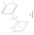
- Cameras having such rectangular CCD have a major disadvantage when photographing a vertical picture. Since the orientation of the picture and the sensor are perpendicular to each other, there is loss of information. This is illustrated in Fig. 3, to which reference is now made.
- a vertical object, referenced 10 is viewed, only part of the object 10 'falls' on the CCD sensor 3, while other parts of the object, indicated by dashed lines 12, are 'lost'.
- the camera is usually rotated 90 , by rotating the base (seating the camera on a conventional tripod, for example).
- rotating the camera base causes misalignment of the camera vis-a-vis the picture being viewed.
- the misalignment is corrected by re-adjusting the stand. This procedure is time-consuming and inconvenient.
- the present invention provides apparatus for moving a CCD sensor in the X-Y direction, which overcomes the limitations and disadvantages of the prior art.
- the present invention further provides orthogonal X-Y movement apparatus, which allows high-resolution color photography in both the X and Y directions, by micro-movement of the CCD sensor.
- the present invention further uses a specific arrangement of the three colors on the CCD sensor, thus providing, in conjunction with the suggested micro-movement of the CCD sensor, a sampling sequence that is optimal for use in a digital camera that may alternately serve as one-shot or three-shot camera.
- the present invention in addition provides a rotatable mount for rotating a CCD sensor within a pre-determined degree of limitation from a first position to a second position, such as 90 degrees from portrait mode to landscape mode, without needing to rotate the camera base and consequent misalignment of the camera.
- the rotatable mount can be used together with the orthogonal X-Y apparatus.
- apparatus for the orthogonal (X,Y) movement of a CCD sensor within a digital camera body which includes a CCD plate to which the CCD sensor is connected, a linear actuator for providing movement in orthogonal X,Y directions to the CCD plate, the linear actuator having a first axis disposed at 45 to the X and Y directions, and means for transferring movement between the linear actuator and the CCD plate.
- the apparatus further includes a base plate connected to the camera body and wire springs connecting the base plate to the CCD plate.
- the means for transferring movement includes a movable member attached to the linear actuator, the actuation of the linear actuator causing the movable member to move either backwards or forwards along the first axis.
- the means for transferring movement further includes first and second rotatable eccentric arms supported by corresponding first and second support rods, respectively, the first and second rotatable eccentric arms being in contact with the CCD plate; and first and second rods, each of the first and second rods having a proximate and a distal end, wherein the distal end of each of the first and second rods is attached to the first and second eccentric arms, respectively, wherein the proximal end of each of the first and second rods is in contact with the movable member, and wherein the proximal end of each of the first and second rods is slidably retained by the base plate.
- the transferring movement means also includes rotatable annuluses fitted to the first and second eccentric arms; and rotating bearings attached to the CCD plate, the rotating bearings in contiguous contact with the rotatable annuluses to reduce friction between the first and second eccentric arms and the CCD plate.
- the first and second rods are in contiguous contact with opposite ends of the movable member; the first rod being positioned behind the movable member proximate to one end of the movable member, and the second rod being positioned in front of the movable member proximate to the other end of the movable member.
- the apparatus further includes first and second restraining plates; each of the first and second restraining plates being attached at a first end to the base plate, and first and second springs attached to the CCD plate and the first and second restraining plates.
- the first restraining plate and the first springs act together to resist movement in the "X"- direction and the second restraining plate and the second springs act together to resist movement in the "Y"- direction.
- a rotatable mount for rotating a CCD sensor within a pre-determined degree of limitation from a first position to a second position.
- the rotatable mount supported by a CCD plate for retaining the CCD sensor, a shaft connected to the rotatable mount and adjustment means attached to the shaft for rotating the CCD plate within a pre-determined degree of limitation.
- the rotatable mount allows the plate to be moved through 90 degrees without the need to adjust the camera base.
- the rotatable mount is supported by means of a plurality of bearings within the CCD plate.
- the rotatable mount further includes a friction ring attached to the shaft for retaining the rotatable mount in position.
- the mount may be rotated either manually using a handle or by a motor.
- a method for sampling the light image from a CCD sensor in a digital camera, having a color filter array includes the steps of:
- the color filter array includes equal resolution for all color channels.
- the color filter array includes one higher resolution color channel.
- the higher resolution color channel may be green.
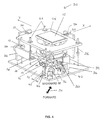
- Fig. 4 is a partially cut-away, partially exploded, isometric view of a bi-dimensional (X-Y) movement apparatus, generally designated 20, constructed and operative according to a preferred embodiment of the present invention.
- the X-Y movement apparatus 20 comprises a base plate 22 for fixing to the camera body (not shown), a CCD plate 24 to which the CCD sensor 15 is attached and a plurality of wire springs 26 connecting base plate 22 to CCD plate 24.
- the wire springs 26 allow the CCD plate 24 to "float" over plate 22 in both the X and Y directions.
- the X-Y movement apparatus of the present invention is characterized by movement means which comprises a linear actuator 38, for example,: model HSI26000 made by HIS Inc, USA, or similar device, and a movable shovel member 36 which is attached to the linear actuator 38.
- Linear actuator 38 is preferably located proximate to one corner of the base plate 22 and the shovel member 36 is disposed perpendicularly to the axes of the linear actuator 38, so that the actuation of linear actuator 38 causes shovel member 36 to move backwards or forwards diagonally across the base plate 22.
- the X-Y movement apparatus further comprises first and second rotatable eccentric arms 28 and 30 supported by members 32 and 34, respectively, and first and second rods 40 and 42, respectively, which are suitably attached at their distal ends 41 to first and second eccentric arms 28 and 30, respectively.
- First and second rotatable eccentric arms 28 and 30 are in contact with CCD plate 24 via annulus 37 for arm 28, and annulus 39 for arm 30.
- the matching bearings attached to plate 24 are referenced no. 13 and 14 while first and second rods 40 and 42 are in contact with the movable shovel member 36.
- First and second rods 40 and 42 are located so as to be in contiguous contact with opposite ends of shovel member 36; first rod 40 being positioned so as to be behind shovel member 36 whereas second rod 42 is positioned to be in front of shovel member 36.
- Support members 32 and 34 extend from the base plate 22 to which they are suitably attached.
- first and second eccentric arms 28 and 30, respectively are supported via bearings not shown to allow the first and second eccentric arms 28 and 30 to freely rotate.
- a rotatable annulus 37 is fitted to first eccentric arm 28 and similarly a second rotatable annulus 39 is fitted to second eccentric arm 30.
- Rotating bearings 13 and 14 are attached to plate 24 and located so as to be in contiguous contact with rotatable annulus 37 and annulus 39, respectively, to reduce friction between the first and second eccentric arms 28 and 30 and the plate 24.
- the minute movement of the actuator is transferred to the CCD plate 24 via the rotating annuluses 37, 39 and bearings 13,14.
- An indentation 44 is formed within base plate 22 to retain the proximate end 45 of first rod 40.
- a spring 46 is located within base plate 22 and is positioned in contiguous contact with the proximate end 45 of first rod 40.
- a second indentation 48 is formed within base plate 22 to retain the proximate end of second rod 42.
- a spring (not shown, similar to screw 46) is located within base plate 22 and is positioned to be contiguous contact with the proximate end of second rod 42. The springs act to return the eccentric arms 28, 30 to their respective original positions when the direction of movement of the linear actuator is changed.
- the X-Y movement apparatus 20 further comprises first and second restraining plates 50 and 52.
- the first restraining plate 50 is attached at one end to base plate 22 and at it's other end by a spring 54 to CCD plate 24.
- First restraining plate 50 and spring 54 act together to resist movement in the "X"-direction.
- second restraining plate 52 which is attached at one end to base plate 22 and at it's other end by a spring 56 to CCD plate 24, resists movement in the "Y"- direction.
- Springs 54 and 56 push plate 24, against first and second eccentric arms 28 and 30, respectively, via the respective bearings.
- the actuator 38 can be moved either backwards or forwards (schematically indicated by arrow 58 which is parallel to diagonal of plate 22).
- the actuator 38 When the actuator 38 is activated forwards, the shovel 36 pushes first rod 40, attached to first eccentric arm 28, thus causing first eccentric arm 28 to rotate and push CCD plate 24 in the X-direction against spring 54.
- the eccentricity of the arms 28 and 30 connected to rods 40 and 42 respectively, and the length of rods 40 and 42, produce a high transmission ratio and thus allow for micro movement of the CCD plate 24. For example, a movement of 0.5 mm by the actuator results in a plate movement of 12 microns.
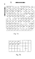
- FIGs. 7A and 7B schematically illustrating the preferred mode of pixel arrangement of a color CCD sensor, to produce optimal sampling resolution according to the sampling method of the present invention (Fig. 7A), and the picture elements being sampled by said CCD elements (Fig. 7B).
- the sampling process according to the present invention enabled by the X-Y movement of the CCD plate as described in conjunction with Figs. 4, 5 and 6, is performed in three stages, so that each pixel of the captured object is sampled through three filters, two of which may be the same color.
- Fig. 7B some of the captured objects' pixels are numbered p1 to p8 for further reference. Let's assume that before starting the capture process, the light reflected from (or passed through) pixel p1 falls on the top-left pixel of the CCD array, and so forth.
- pixels p1 to p8 After the first capture, the following information will have been sampled in reference to pixels p1 to p8: R(p1), G(p2), R(p3), G(p4), G(p5), B(p6), G(p7), B(p8).
- the CCD is moved along, say, the X-axis, a distance that is equal to the size of one CCD cell in the direction of the movement, and a second capture is taken.
- the CCD is moved along the perpendicular, say, Y axis a distance that is equal to the size of one CCD cell in the direction of the movement, and a third capture is taken.
- pixels p1 to p8 After the third capture, the following information will have been sampled in reference to pixels p1 to p8: RGG(p1), RGB(p2), RGG(p3), RGB(p4), RGB(p5), GGB(p6), RGB(p7), GGB(p8).
- half of the pixels have full color information (RGB) and the other half only have information from two of the color channels.
- the higher resolution channel will capture detail that is missed by lower resolution channels.
- interpolation is first done on the data of the high-resolution channel, and then the other missing channels are interpolated at each pixel location, by assuming color constancy over local areas.
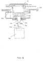
- Fig. 5 is an isometric view of a rotatable mount, constructed and operative according to a preferred embodiment of the present invention and Fig. 6 is a sectional view of the rotatable mount of Fig. 5.
- Rotatable mount 70 is connected by means of a shaft 72 extending below the base plate 22 to a manual lever 74.
- a motor 76 can be attached to the shaft 72.
- the rotatable mount 70 is held within the CCD plate 24 by means of a plurality of bearings 78, 79 allowing the CCD plate 24 to rotate within a pre-determined degree of limitation, preferably 90 degrees (indicated by reference 81.
- a friction ring 80 suitably attached to shaft 72, retains rotatable mount 70 in place.
- CCD plate 24 can be actuated (either manually by lever 74 or by motor 76 ) to rotate through 90 degrees from a first position (say portrait mode) to a second position (say landscape mode) at right angles to the first position.
- actuated either manually by lever 74 or by motor 76
- the misalignment of the camera is avoided and it is no longer necessary to re-adjusting the camera stand.
Landscapes
- Engineering & Computer Science (AREA)
- Multimedia (AREA)
- Signal Processing (AREA)
- Transforming Light Signals Into Electric Signals (AREA)
- Color Television Image Signal Generators (AREA)
Applications Claiming Priority (2)
| Application Number | Priority Date | Filing Date | Title |
|---|---|---|---|
| IL12616598 | 1998-09-10 | ||
| IL12616598A IL126165A0 (en) | 1998-09-10 | 1998-09-10 | Apparatus for the orthogonal movement of a ccd sensor |
Publications (2)
| Publication Number | Publication Date |
|---|---|
| EP0986251A2 true EP0986251A2 (de) | 2000-03-15 |
| EP0986251A3 EP0986251A3 (de) | 2001-08-01 |
Family
ID=11071953
Family Applications (1)
| Application Number | Title | Priority Date | Filing Date |
|---|---|---|---|
| EP99303503A Withdrawn EP0986251A3 (de) | 1998-09-10 | 1999-05-05 | Vorrichtung zur orthogonalen Bewegung eines CCD Sensors und Methode zur Lichtabtastung damit |
Country Status (3)
| Country | Link |
|---|---|
| US (1) | US6670986B1 (de) |
| EP (1) | EP0986251A3 (de) |
| IL (1) | IL126165A0 (de) |
Cited By (5)
| Publication number | Priority date | Publication date | Assignee | Title |
|---|---|---|---|---|
| GB2399704B (en) * | 2003-02-20 | 2006-09-27 | Hewlett Packard Development Co | Systems and methods for providing multiple object planes in an optical image scanner |
| CN102703301A (zh) * | 2012-05-24 | 2012-10-03 | 中国科学院北京基因组研究所 | 用于测序芯片的安装座与ccd相机间的暗室 |
| CN102703311A (zh) * | 2012-05-24 | 2012-10-03 | 中国科学院北京基因组研究所 | 用于dna测序仪的自适应调整的反应仓 |
| CN102703302A (zh) * | 2012-05-24 | 2012-10-03 | 中国科学院北京基因组研究所 | 自动卡持测序芯片的安装座 |
| US9280037B2 (en) | 2012-05-03 | 2016-03-08 | Serview, Inc. | Machine vision camera mount with rotational adjustment |
Families Citing this family (55)
| Publication number | Priority date | Publication date | Assignee | Title |
|---|---|---|---|---|
| US6967677B1 (en) * | 2000-09-15 | 2005-11-22 | Sinar Ag | Microscan guidance |
| JP2002176581A (ja) * | 2000-12-05 | 2002-06-21 | Funai Electric Co Ltd | 電子写真装置 |
| US7657123B2 (en) * | 2001-10-03 | 2010-02-02 | Microsoft Corporation | Text document capture with jittered digital camera |
| US6824317B2 (en) * | 2001-11-21 | 2004-11-30 | Thales Avionics, Inc. | Universal security camera |
| US6970608B1 (en) * | 2001-12-30 | 2005-11-29 | Cognex Technology And Investment Corporation | Method for obtaining high-resolution performance from a single-chip color image sensor |
| JP2004266709A (ja) * | 2003-03-04 | 2004-09-24 | Victor Co Of Japan Ltd | 撮像装置 |
| JP2005077886A (ja) * | 2003-09-02 | 2005-03-24 | Canon Inc | 撮影装置 |
| US6934065B2 (en) * | 2003-09-18 | 2005-08-23 | Micron Technology, Inc. | Microelectronic devices and methods for packaging microelectronic devices |
| US7583862B2 (en) * | 2003-11-26 | 2009-09-01 | Aptina Imaging Corporation | Packaged microelectronic imagers and methods of packaging microelectronic imagers |
| US7580559B2 (en) * | 2004-01-29 | 2009-08-25 | Asml Holding N.V. | System and method for calibrating a spatial light modulator |
| US7253397B2 (en) * | 2004-02-23 | 2007-08-07 | Micron Technology, Inc. | Packaged microelectronic imagers and methods of packaging microelectronic imagers |
| US7253957B2 (en) * | 2004-05-13 | 2007-08-07 | Micron Technology, Inc. | Integrated optics units and methods of manufacturing integrated optics units for use with microelectronic imagers |
| US8092734B2 (en) | 2004-05-13 | 2012-01-10 | Aptina Imaging Corporation | Covers for microelectronic imagers and methods for wafer-level packaging of microelectronics imagers |
| US7742076B2 (en) * | 2004-05-25 | 2010-06-22 | Hoya Corporation | Image-capturing apparatus and camera-shake compensation mechanism |
| US20050275750A1 (en) * | 2004-06-09 | 2005-12-15 | Salman Akram | Wafer-level packaged microelectronic imagers and processes for wafer-level packaging |
| US7498647B2 (en) | 2004-06-10 | 2009-03-03 | Micron Technology, Inc. | Packaged microelectronic imagers and methods of packaging microelectronic imagers |
| US7199439B2 (en) * | 2004-06-14 | 2007-04-03 | Micron Technology, Inc. | Microelectronic imagers and methods of packaging microelectronic imagers |
| US7262405B2 (en) * | 2004-06-14 | 2007-08-28 | Micron Technology, Inc. | Prefabricated housings for microelectronic imagers |
| US7294897B2 (en) * | 2004-06-29 | 2007-11-13 | Micron Technology, Inc. | Packaged microelectronic imagers and methods of packaging microelectronic imagers |
| US7232754B2 (en) | 2004-06-29 | 2007-06-19 | Micron Technology, Inc. | Microelectronic devices and methods for forming interconnects in microelectronic devices |
| US7416913B2 (en) * | 2004-07-16 | 2008-08-26 | Micron Technology, Inc. | Methods of manufacturing microelectronic imaging units with discrete standoffs |
| US7189954B2 (en) * | 2004-07-19 | 2007-03-13 | Micron Technology, Inc. | Microelectronic imagers with optical devices and methods of manufacturing such microelectronic imagers |
| US7402453B2 (en) * | 2004-07-28 | 2008-07-22 | Micron Technology, Inc. | Microelectronic imaging units and methods of manufacturing microelectronic imaging units |
| US7364934B2 (en) | 2004-08-10 | 2008-04-29 | Micron Technology, Inc. | Microelectronic imaging units and methods of manufacturing microelectronic imaging units |
| US7397066B2 (en) * | 2004-08-19 | 2008-07-08 | Micron Technology, Inc. | Microelectronic imagers with curved image sensors and methods for manufacturing microelectronic imagers |
| US7223626B2 (en) * | 2004-08-19 | 2007-05-29 | Micron Technology, Inc. | Spacers for packaged microelectronic imagers and methods of making and using spacers for wafer-level packaging of imagers |
| US7429494B2 (en) * | 2004-08-24 | 2008-09-30 | Micron Technology, Inc. | Microelectronic imagers with optical devices having integral reference features and methods for manufacturing such microelectronic imagers |
| US7115961B2 (en) * | 2004-08-24 | 2006-10-03 | Micron Technology, Inc. | Packaged microelectronic imaging devices and methods of packaging microelectronic imaging devices |
| US7425499B2 (en) | 2004-08-24 | 2008-09-16 | Micron Technology, Inc. | Methods for forming interconnects in vias and microelectronic workpieces including such interconnects |
| US7276393B2 (en) * | 2004-08-26 | 2007-10-02 | Micron Technology, Inc. | Microelectronic imaging units and methods of manufacturing microelectronic imaging units |
| US20070148807A1 (en) | 2005-08-22 | 2007-06-28 | Salman Akram | Microelectronic imagers with integrated optical devices and methods for manufacturing such microelectronic imagers |
| US7511262B2 (en) * | 2004-08-30 | 2009-03-31 | Micron Technology, Inc. | Optical device and assembly for use with imaging dies, and wafer-label imager assembly |
| US7646075B2 (en) * | 2004-08-31 | 2010-01-12 | Micron Technology, Inc. | Microelectronic imagers having front side contacts |
| US7300857B2 (en) * | 2004-09-02 | 2007-11-27 | Micron Technology, Inc. | Through-wafer interconnects for photoimager and memory wafers |
| US7271482B2 (en) | 2004-12-30 | 2007-09-18 | Micron Technology, Inc. | Methods for forming interconnects in microelectronic workpieces and microelectronic workpieces formed using such methods |
| US7214919B2 (en) * | 2005-02-08 | 2007-05-08 | Micron Technology, Inc. | Microelectronic imaging units and methods of manufacturing microelectronic imaging units |
| US7303931B2 (en) * | 2005-02-10 | 2007-12-04 | Micron Technology, Inc. | Microfeature workpieces having microlenses and methods of forming microlenses on microfeature workpieces |
| US7190039B2 (en) * | 2005-02-18 | 2007-03-13 | Micron Technology, Inc. | Microelectronic imagers with shaped image sensors and methods for manufacturing microelectronic imagers |
| US7795134B2 (en) | 2005-06-28 | 2010-09-14 | Micron Technology, Inc. | Conductive interconnect structures and formation methods using supercritical fluids |
| JP4508010B2 (ja) * | 2005-06-30 | 2010-07-21 | パナソニック株式会社 | 撮像素子駆動装置およびそれを用いた撮影装置 |
| US7288757B2 (en) * | 2005-09-01 | 2007-10-30 | Micron Technology, Inc. | Microelectronic imaging devices and associated methods for attaching transmissive elements |
| US7262134B2 (en) | 2005-09-01 | 2007-08-28 | Micron Technology, Inc. | Microfeature workpieces and methods for forming interconnects in microfeature workpieces |
| US7622377B2 (en) | 2005-09-01 | 2009-11-24 | Micron Technology, Inc. | Microfeature workpiece substrates having through-substrate vias, and associated methods of formation |
| US7903302B2 (en) * | 2007-10-01 | 2011-03-08 | Kabushiki Kaisha Toshiba | Image reading apparatus and image reading method |
| US8169519B1 (en) * | 2007-12-26 | 2012-05-01 | Google Inc. | System and method for reducing motion blur using CCD charge shifting |
| US8358372B2 (en) * | 2008-06-23 | 2013-01-22 | Eastman Kodak Company | Digital camera curved flat cable |
| KR101013156B1 (ko) * | 2008-10-10 | 2011-02-10 | 한국기계연구원 | 전동줌렌즈와 회전미러를 이용한 고속 광학관측 시스템 |
| KR101499540B1 (ko) * | 2008-10-24 | 2015-03-06 | 삼성전자주식회사 | 이미지 촬상 장치와 이를 이용한 이미지 처리 방법 |
| US20100194465A1 (en) * | 2009-02-02 | 2010-08-05 | Ali Salih | Temperature compensated current source and method therefor |
| CN101938600B (zh) * | 2009-06-29 | 2012-09-19 | 鸿富锦精密工业(深圳)有限公司 | 摄像装置 |
| TWI386043B (zh) * | 2009-07-10 | 2013-02-11 | Hon Hai Prec Ind Co Ltd | 攝像裝置 |
| EP3091384B1 (de) | 2014-01-02 | 2023-04-12 | LG Innotek Co., Ltd. | Linsenansteuerungsvorrichtung und kameramodul damit |
| JP5893712B1 (ja) * | 2014-11-04 | 2016-03-23 | オリンパス株式会社 | 撮像装置、撮像方法、処理プログラム |
| CN112616007B (zh) * | 2020-12-31 | 2022-06-17 | 维沃移动通信有限公司 | 电子设备及其摄像模组 |
| CN113592810B (zh) * | 2021-07-29 | 2022-04-19 | 东莞市亚太未来软件有限公司 | 一种基于图像数据处理的学生学习数据筛选方法、设备 |
Family Cites Families (12)
| Publication number | Priority date | Publication date | Assignee | Title |
|---|---|---|---|---|
| JPS56153693A (en) | 1980-04-30 | 1981-11-27 | Matsushita Electric Works Ltd | Device for firing discharge lamp |
| JPS6198073A (ja) | 1984-10-19 | 1986-05-16 | Hitachi Ltd | 撮像装置 |
| US4803557A (en) * | 1988-01-11 | 1989-02-07 | Eastman Kodak Company | Adjustable mount for image sensor |
| JPH01251965A (ja) | 1988-03-31 | 1989-10-06 | Toshiba Corp | 固体撮像装置 |
| DE3837063C1 (de) | 1988-10-31 | 1990-03-29 | Reimar Dr. 8000 Muenchen De Lenz | |
| US5214513A (en) * | 1991-07-11 | 1993-05-25 | Eastman Kodak Company | Apparatus for imparting motion to a solid-state image sensor |
| JP3238498B2 (ja) * | 1992-09-14 | 2001-12-17 | コーニンクレッカ フィリップス エレクトロニクス エヌ ヴィ | 固体影像記録装置 |
| JPH06189318A (ja) | 1992-12-22 | 1994-07-08 | Kyocera Corp | 映像機器用のカラ−撮像装置 |
| US5640207A (en) * | 1993-05-19 | 1997-06-17 | Rahmouni; Gilbert | Camera for high-speed imaging |
| KR0150980B1 (ko) * | 1993-12-24 | 1998-10-15 | 김광호 | 카메라 |
| JPH10126663A (ja) * | 1996-10-14 | 1998-05-15 | Ricoh Co Ltd | 画像入力装置及び画像入力システム |
| JP3704238B2 (ja) * | 1997-03-31 | 2005-10-12 | 株式会社リコー | 撮像装置 |
-
1998
- 1998-09-10 IL IL12616598A patent/IL126165A0/xx unknown
-
1999
- 1999-04-29 US US09/301,548 patent/US6670986B1/en not_active Expired - Lifetime
- 1999-05-05 EP EP99303503A patent/EP0986251A3/de not_active Withdrawn
Cited By (7)
| Publication number | Priority date | Publication date | Assignee | Title |
|---|---|---|---|---|
| GB2399704B (en) * | 2003-02-20 | 2006-09-27 | Hewlett Packard Development Co | Systems and methods for providing multiple object planes in an optical image scanner |
| US9280037B2 (en) | 2012-05-03 | 2016-03-08 | Serview, Inc. | Machine vision camera mount with rotational adjustment |
| CN102703301A (zh) * | 2012-05-24 | 2012-10-03 | 中国科学院北京基因组研究所 | 用于测序芯片的安装座与ccd相机间的暗室 |
| CN102703311A (zh) * | 2012-05-24 | 2012-10-03 | 中国科学院北京基因组研究所 | 用于dna测序仪的自适应调整的反应仓 |
| CN102703302A (zh) * | 2012-05-24 | 2012-10-03 | 中国科学院北京基因组研究所 | 自动卡持测序芯片的安装座 |
| CN102703311B (zh) * | 2012-05-24 | 2013-08-21 | 中国科学院北京基因组研究所 | 用于dna测序仪的自适应调整的反应仓 |
| CN102703302B (zh) * | 2012-05-24 | 2013-11-27 | 中国科学院北京基因组研究所 | 自动卡持测序芯片的安装座 |
Also Published As
| Publication number | Publication date |
|---|---|
| EP0986251A3 (de) | 2001-08-01 |
| US6670986B1 (en) | 2003-12-30 |
| IL126165A0 (en) | 1999-05-09 |
Similar Documents
| Publication | Publication Date | Title |
|---|---|---|
| US6670986B1 (en) | Apparatus for orthogonal movement of a CCD sensor and a method of light sampling therewith | |
| US8059185B2 (en) | Photographing apparatus, image display method, computer program and storage medium for acquiring a photographed image in a wide range | |
| JPH06350931A (ja) | 固体撮像装置 | |
| JPH03502755A (ja) | 光電カラーイメージセンサ | |
| US20050093891A1 (en) | Image orientation apparatus and method | |
| JPH0614750B2 (ja) | カラ−原稿撮像装置 | |
| JP3523667B2 (ja) | 複眼式光学系 | |
| JPH10200804A (ja) | カメラ型スキャナ | |
| EP1964060A1 (de) | Digital-panorama-kamera | |
| US7129460B1 (en) | Electronic imaging apparatus with high resolution and wide field of view and method | |
| JP2003101733A (ja) | 画像読取装置 | |
| US6686956B1 (en) | Increased resolution digital capture device | |
| HK1052977A1 (zh) | 建立預選柱鏡圖像的方法和裝置 | |
| JPH06292052A (ja) | 静止画像撮像装置 | |
| JP3027915B2 (ja) | イメージスキャナとその画像読込み方法 | |
| JP2002218510A (ja) | 3d画像取得装置 | |
| JP3724701B2 (ja) | 固体撮像装置及び解像度変換装置 | |
| JPH07503113A (ja) | 多重副画像を捕捉するための光学的偏向要素を備える画像入力装置 | |
| JP3052160B2 (ja) | 固体撮像素子 | |
| JP4043091B2 (ja) | 画像入力方法、画像入力装置、電子カメラ | |
| JPH09261545A (ja) | 画像入力装置 | |
| JP3134820B2 (ja) | 撮像方法および撮像装置 | |
| JP4272823B2 (ja) | 撮像装置 | |
| JP4549255B2 (ja) | 固体撮像装置及び解像度変換装置 | |
| JP4517292B2 (ja) | 面順次カラー画像撮像装置 |
Legal Events
| Date | Code | Title | Description |
|---|---|---|---|
| PUAI | Public reference made under article 153(3) epc to a published international application that has entered the european phase |
Free format text: ORIGINAL CODE: 0009012 |
|
| AK | Designated contracting states |
Kind code of ref document: A2 Designated state(s): BE DE FR GB |
|
| AX | Request for extension of the european patent |
Free format text: AL;LT;LV;MK;RO;SI |
|
| RAP1 | Party data changed (applicant data changed or rights of an application transferred) |
Owner name: CREOSCITEX CORPORATION LTD. |
|
| PUAL | Search report despatched |
Free format text: ORIGINAL CODE: 0009013 |
|
| AK | Designated contracting states |
Kind code of ref document: A3 Designated state(s): AT BE CH CY DE DK ES FI FR GB GR IE IT LI LU MC NL PT SE |
|
| AX | Request for extension of the european patent |
Free format text: AL;LT;LV;MK;RO;SI |
|
| 17P | Request for examination filed |
Effective date: 20010830 |
|
| AKX | Designation fees paid |
Free format text: BE DE FR GB |
|
| RAP1 | Party data changed (applicant data changed or rights of an application transferred) |
Owner name: CREO IL. LTD. |
|
| 17Q | First examination report despatched |
Effective date: 20041214 |
|
| STAA | Information on the status of an ep patent application or granted ep patent |
Free format text: STATUS: THE APPLICATION IS DEEMED TO BE WITHDRAWN |
|
| 18D | Application deemed to be withdrawn |
Effective date: 20050426 |