EP0987864A1 - Zeitfehlerkompensationsanordnung und diese umfassendes Mehrträgermodem - Google Patents
Zeitfehlerkompensationsanordnung und diese umfassendes Mehrträgermodem Download PDFInfo
- Publication number
- EP0987864A1 EP0987864A1 EP98402272A EP98402272A EP0987864A1 EP 0987864 A1 EP0987864 A1 EP 0987864A1 EP 98402272 A EP98402272 A EP 98402272A EP 98402272 A EP98402272 A EP 98402272A EP 0987864 A1 EP0987864 A1 EP 0987864A1
- Authority
- EP
- European Patent Office
- Prior art keywords
- time error
- filter
- time
- receiver
- input terminal
- Prior art date
- Legal status (The legal status is an assumption and is not a legal conclusion. Google has not performed a legal analysis and makes no representation as to the accuracy of the status listed.)
- Withdrawn
Links
- 238000004422 calculation algorithm Methods 0.000 description 8
- 239000000969 carrier Substances 0.000 description 6
- 238000004364 calculation method Methods 0.000 description 5
- 238000000034 method Methods 0.000 description 3
- 102100034033 Alpha-adducin Human genes 0.000 description 2
- 101000799076 Homo sapiens Alpha-adducin Proteins 0.000 description 2
- 101000629598 Rattus norvegicus Sterol regulatory element-binding protein 1 Proteins 0.000 description 2
- 238000001914 filtration Methods 0.000 description 2
- 238000007792 addition Methods 0.000 description 1
- 230000005540 biological transmission Effects 0.000 description 1
- 230000008878 coupling Effects 0.000 description 1
- 238000010168 coupling process Methods 0.000 description 1
- 238000005859 coupling reaction Methods 0.000 description 1
- 230000006735 deficit Effects 0.000 description 1
- 238000010586 diagram Methods 0.000 description 1
- 238000009533 lab test Methods 0.000 description 1
- 238000004088 simulation Methods 0.000 description 1
- 230000001360 synchronised effect Effects 0.000 description 1
Images


Classifications
-
- H—ELECTRICITY
- H04—ELECTRIC COMMUNICATION TECHNIQUE
- H04L—TRANSMISSION OF DIGITAL INFORMATION, e.g. TELEGRAPHIC COMMUNICATION
- H04L7/00—Arrangements for synchronising receiver with transmitter
-
- H—ELECTRICITY
- H04—ELECTRIC COMMUNICATION TECHNIQUE
- H04L—TRANSMISSION OF DIGITAL INFORMATION, e.g. TELEGRAPHIC COMMUNICATION
- H04L27/00—Modulated-carrier systems
- H04L27/26—Systems using multi-frequency codes
- H04L27/2601—Multicarrier modulation systems
- H04L27/2647—Arrangements specific to the receiver only
- H04L27/2655—Synchronisation arrangements
- H04L27/2657—Carrier synchronisation
-
- H—ELECTRICITY
- H04—ELECTRIC COMMUNICATION TECHNIQUE
- H04L—TRANSMISSION OF DIGITAL INFORMATION, e.g. TELEGRAPHIC COMMUNICATION
- H04L27/00—Modulated-carrier systems
- H04L27/26—Systems using multi-frequency codes
- H04L27/2601—Multicarrier modulation systems
- H04L27/2647—Arrangements specific to the receiver only
- H04L27/2655—Synchronisation arrangements
- H04L27/2662—Symbol synchronisation
Definitions
- the present invention relates to a time error compensation arrangement as defined in the non-characteristic part of claim 1, and a multi-carrier receiver comprising such a time error compensation arrangement as defined in the non-characteristic part of claim 5.
- a time error compensation arrangement and a multi-carrier receiver including such a time error compensation arrangement are already known in the art, e.g. from the United States patent US 5,228,062, entitled 'Method and Apparatus for Correcting for Clock and Carrier Frequency Offset, and Phase Jitter in Multicarrier Modems'. More paticularly, Fig. 2 of US 5,228,062 shows a multi-carrier modem including circuitry to detect a time error resulting from a frequency difference between a transmitter clock and receiver clock, phase jitter impairments, etc. , and including a digital filter - named interpolator and referred to by 310 in Fig. 2 of US 5,228,062 - to compensate for the detected time error.
- An object of the present invention is to provide a time error compensation arrangement, and related multi-carrier receiver and time error compensating method of the above known type, but whose complexity in terms of amount of filter coefficients required to compensate for a given time error with a given accuracy, and the mathematical complexity of an algorithm for updating the filter coefficients, is reduced significantly.
- this object is achieved by the time error compensation arrangement defined in claim 1 and the multi-carrier receiver defined in claim 5.
- the digital time correction filter in the arrangement according to the present invention only compensates for the linearly incrementing contribution in the detected time error that results from the time frequency difference between the transmitter clock and frequency clock.
- a linearly increasing time error can be compensated for by a digital filter, operative in time domain, with low complexity.
- the filter coefficients thereto may be adjusted continuously in accordance with a filter coefficient updating algorithm. Such algorithms are well known in the art.
- the remaining contribution to the time error which is an integer times (N-1). ⁇ k in case the linearly incrementing contribution to be compensated for by the digital filter is limited to (N-1). ⁇ k - N being the amount of samples in a multi-carrier symbol and ⁇ k being the linear increment of the time error - is compensated for in frequency domain by a rotor such as the one known from European Patent Application EP 0 820 171, entitled 'Multicarrier transmitter or receiver with phase rotators'.
- the term 'coupled' should not be interpreted as being limitative to direct connections only.
- the scope of the expression 'a device A coupled to a device B' should not be limited to devices or systems wherein an output of device A is directly connected to an input of device B. It means that there exists a path between an output of A and an input of B which may be a path including other devices or means.
- the digital time correction filter comprises a parallel structure of digital filters having constant filter coefficients.
- the outputs of these parallel digital filters are scaled with scale factors that are time variable so that changes in clock speed difference between the transmitter clock and receiver clock can be countered by suitably adapting the scale factors.
- the scale factors as will be shown later in this application, have a simple relation to the time error between transmitter and receiver so that no complex algorithm is required for updating the scale factors and no updating algorithm at all is required for the filter coefficients which are constant now.
- ADSL Asymmetric Digital Subscriber Line
- VDSL Very High Speed Digital Subscriber Line
- a time error between the multi-carrier DMT (Discrete Multi Tone) modem at the central office and the multi-carrier DMT (Discrete Multi Tone) modem at the remote client can be compensated for by a arrangement according to the present invention with time invariable filter coefficients and reduced architectural complexity.
- a Farrow architecture with six filter coefficients and 1 adaptable scale factor is sufficient for time error compensation in such an environment, as will be proven later in this document.
- the multi-carrier receiver RX1 drawn in Fig. 1 includes an analogue to digital converter ADC, a receiver clock CLK, a fourier transformer FFT, and a time error compensation arrangement TCOMP.
- the latter time error compensation arrangement TCOMP contains a digital time correction filter FILTER and a phase rotor ROTOR.
- the analogue to digital converter ADC, the digital time correction filter FILTER, the fourier transformer FFT and the phase rotor ROTOR are cascade coupled between an input terminal and an output terminal of the multi-carrier receiver RX1.
- An output of the receiver clock CLK is interconnected with a clock input of the analogue to digital converter ADC.
- the multi-carrier receiver RX1 in addition to the drawn components at least also contains a time error detector, for instance a digital phase locked loop, whose output is connected to a time error input terminal of the time error compensation arrangement TCOMP. Because the present invention is not concerned with the method used to detect the time error, this time error detector is not drawn in Fig. 1.
- the time error input terminal of the time error compensation arrangement TCOMP is referred to by ⁇ , ⁇ k and is internally connected to control inputs of both the digital time correction filter FILTER and the phase rotor ROTOR in the time error compensation arrangement TCOMP.
- the analogue to digital converter ADC samples an incoming multi-carrier signal s(t) and thereby generates a sample sequence s(n). Subsets of samples of this sample sequence s(n) are then digitally filtered by the digital time correction filter FILTER which thereby generates a time corrected sample sequence sc(n).
- the time corrected sample sequence sc(n) at the output of the digital time correction filter FILTER is transformed from time domain to frequency domain by the fourier transformer FFT which produces at its output a set of modulated carriers SC(n).
- the phases of the carriers in this set of modulated carriers SC(n) are rotated by the phase rotor ROTOR over an angle in proportion to the frequencies of the respective carriers so that a final time correction is applied.
- the so obtained frequency domain signal can be demapped if the constellation scheme used for modulation of the carriers in the transmitter that has sent the multi-carrier signal s(t) to receiver RX1 is known.
- the elements in the receiver RX1 responsible for demapping the carriers are not shown in Fig. 1 because their precise working is well known in the art and irrelevant in view of the present invention.
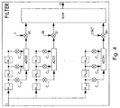
- the multi-carrier receiver RX2 drawn in Fig. 2 differs from the receiver RX1 drawn in Fig. 1 in that it includes a downsampler DSAMP, coupled between the digital time correction filter FILTER' and the fourier transformer FFT.
- the functional blocks ADC, CLK, FFT, TCOMP and ROTOR have the same functionality as the equally named functional blocks in the receiver RX1 of Fig. 1.
- the only difference is that the clock signal produced by the receiver clock CLK has a higher frequency, e.g. the double of the frequency of the clock signal produced by the receiver clock CLK in Fig. 1, so that the analogue to digital converter ADC samples the incoming multi-carrier signal s(t) at the double sample frequency.
- the thereby produced sample sequence s(n) is again digitally filtered by a digital time correction filter FILTER' which is described in more detail by Fig. 4, and the so obtained time corrected sample sequence sc(n) is downsampled by a factor 2 in the downsampler DSAMP.
- the time domain samples consequently appear with the same speed at the input of the fourier transformer FFT as in Fig. 1.
- the upsampling by ADC and downsampling by DSAMP help to reduce the amplitude distortion due to digital filtering in the digital time correction filter FILTER'.
- the digital time correction filter FILTER in the multi-carrier receivers RX1 of Fig. 1 is drawn in Fig. 3 and has time variable filter coefficients C -1 , C 0 and C 1 .
- the digital time correction filter FILTER drawn in Fig. 3 includes three memory cells M -1 , M 0 , M 1 each capable of storing a sample of the sample sequence s(n) in Fig. 1, three multipliers C -1 , C 0 and C 1 representing the time variable filter coefficients, and an adder ADD.
- the memory cells M -1 , M 0 and M 1 are cascade connected, the signal input I of the digital time correction filter FILTER serving as an input for the first memory cell M -1 .
- the outputs of the memory cells M -1 , M 0 and M 1 are connected to inputs of the multipliers C -1 , C 0 and C 1 respectively, and outputs of these multipliers C -1 , C 0 and C 1 are connected to input terminals of the adder ADD.
- An output of the adder ADD serves as output terminal O for the digital time correction filter FILTER.
- time error input terminal ⁇ , ⁇ k of the digital time correction filter FILTER in Fig. 1 is coupled via a calculation unit to control inputs of the multipliers C -1 , C 0 and C 1 .
- This coupling and the calculation unit are not drawn in Fig. 3.
- the calculation unit converts the linearly incrementing contribution to the time error into suitable filter coefficient values C -1 , C 0 and C 1 .
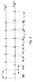
- the working of the digital time correction filter FILTER of Fig. 3 is best described with reference to Fig. 5.
- the points labelled 0, 1, 2, 3, 4, 5, 6 and 7 on the time axis TX Time represent sample times of the multi-carrier transmitter communicating with the receiver RX1 of Fig. 1, for the same multi-carrier symbol.
- This multi-carrier transmitter includes a transmitter clock with sample period T T .
- the points labelled 0', 1', 2', 3', 4', 5', 6' and 7' on the time axis RX Time represent sample times of the multi-carrier receiver, RX1 of Fig. 1.
- the multi-carrier receiver RX1 includes a receiver clock CLK with sample period T R .
- the transmitter clock and the receiver clock CLK are supposed to be fixed, uncontrollable clocks. As a consequence, there is a clock frequency difference between the transmitter clock and the receiver clock CLK as a result of which the time error between the receiver sample times 0', 1', 2', 3', 4', 5', 6' and 7' and the transmitter sample times 0, 1, 2, 3, 4, 5, 6 and 7 is linearly incrementing. This time error is indicated in Fig. 5 by ⁇ 0, ⁇ 1, ⁇ 2, ⁇ 3, ⁇ 4, ⁇ 5, ⁇ 6 and ⁇ 7.
- the digital time correction filter FILTER has to compensate for the linearly incrementing contribution i. ⁇ k.
- the remaining contribution ⁇ to the time error is compensated for by the phase rotor ROTOR in multi-carrier receiver RX1 and typically equals an integer times N. ⁇ k where N is the number of samples in a multi-carrier symbol.
- the digital time correction filter FILTER thus has to compensate for a time error which increases stepwise from zero to (N-1). ⁇ k, N being the number of samples per symbol.
- the digital time correction filter FILTER thereto transforms a subset of three samples s(n) generated by the analogue to digital converter ADC in multi-carrier receiver RX1 into a time corrected sample sc(n) which would have been obtained by receiver RX1 if the receiver clock CLK and transmitter clock would have been synchronised.
- the samples generated in multi-carrier receiver RX1 at sample times 3', 4' and 5' for example are linearly combined by the digital filter FILTER to generate the sample that should have been obtained by receiver RX1 at sample time 4.
- the samples generated in multi-carrier receiver RX1 at sample times 4', 5' and 6' are linearly combined by the digital filter FILTER to generate the sample that should have been obtained by receiver RX1 at sample time 5, and so on.
- the digital time correction filter FILTER thereto multiplies the sample at sample time 3' with a filter coefficient C -1 , the sample at sample time 4' with a filter coefficient C 0 and the sample at sample time 5' with a filter coefficient C 1 .
- the adder ADD sums the scaled samples to produce the sample at sample time 4.
- the filter coefficients C -1 , C 0 and C 1 are suitably determined by the already mentioned calculation unit which thereto uses well-known algorithms.
- the number of filter coefficients required in the digital time correction filter FILTER can be kept reasonable because the filter FILTER only compensates for the linearly increasing contribution i. ⁇ k of the time error due to the clock speed difference between transmitter clock and receiver clock CLK.
- the remaining contribution to the time error ⁇ is, as already mentioned, compensated for by the phase rotor ROTOR in the multi-carrier receiver RX1. It is this aspect of the invention that is particularly advantageous because it makes time error compensation in a multi-carrier environment feasible without the necessity to have a voltage controlled clock in either the transmitter or the receiver.
- the digital time correction filter FILTER' drawn in Fig. 4 contains memory cells M -1,0 , M -1,1 , ..., M -1,N , M 0,0 , M 0,1 , ..., ..., M 0,N , M 1,0 , M 1,1 , ..., M 1,N , filter coefficient multipliers C -1,0 , C -1,1 , ...,C -1,N , C 0,0 , C 0,1 , ..., C 0,N , C 1,0 , C 1,1 , ..., C 1,N , adders ADD0, ADD1, ..., ADDN, scaling means S0, S1, ..., SN, and a summator SUM.
- the memory cells M -1,0 , M 0,0 , M 1,0 , the filter coefficient multipliers C -1,0 , C 0,0 , C 1,0 , and the adder ADD0 constitute a first filter.
- the memory cells M -1,0 , M 0,0 , and M 1,0 are cascade coupled, the input of the first memory cell M -1,0 being interconnected with the input terminal I of the digital time error correction filter FILTER'.
- Outputs of the memory cells M -1,0 , M 0,0 , and M 1,0 are connected to inputs of the filter coefficient multipliers C -1,0 , C 0,0 and C 1,0 respectively and outputs of the latter filter coefficient multipliers C -1,0 , C 0,0 and C 1,0 serve as inputs for the adder ADD0.
- the memory cells M -1,1 , M 0,1 , M 1,1 , the filter coefficient multipliers C -1,1 , C 0,1 , C 1,1 and the adder ADD1 are arranged into a second filter with the same structure as the just described one and also the memory cells M -1,N , M 0,N , M 1,N , the filter coefficient multipliers C -1,N , C 0,N , C 1,N and the adder ADDN constitute a filter with this structure.
- the just described filters are all parallel coupled between the input terminal I of the digital time correction filter FILTER' and the summator SUM, but between the parallel filters and the summator SUM, the scaling means S0, S1, ..., SN are inserted respectively.
- the output of the summator SUM is internally connected with the output terminal O of the digital time correction filter FILTER.
- These scaling means S0, S1, ..., SN have scale factors 1, ⁇ k, ..., ( ⁇ k) N , that depend on the measured time error and consequently are interconnected via control lines with the time error input terminal ⁇ , ⁇ k of the time error compensation arrangement TCOMP where the filter FILTER' forms part of. These control connections are not drawn in any of the figures.
- the digital time correction filter FILTER' shown in detail in Fig. 4 is even more feasible than the digital time correction filter FILTER of Fig. 1 and Fig. 3, described earlier. This is so because the filter coefficients C -1,0 , C -1,1 , ..., C -1,N , C 0,0 , C 0,1 , ..., C 0,N , C 1,0 , C 1,1 , ..., C 1,N , of the digital time correction filter FILTER' in Fig. 4 are time invariable so that the above mentioned calculation unit no longer has to determine suitable filter coefficients by applying a well-known algorithm. This simplification is obtained by implementing the digital time correction filter FILTER' with a Farrow architecture.
- such a Farrow architecture is a parallel structure of digital filters with predetermined filter coefficients C -1,0 , C -1,1 , ..., C -1,N , C 0,0 , C 0,1 , ..., C 0,N , C 1,0 , C 1,1 , ..., C 1,N , each scaled by a scale factor S0, S1, ..., SN which is time variable but which has a simple relation to the measured linear increment ⁇ k of the time error between transmitter and receiver sample clocks.
- the value of the filter coefficients C -1,0 , C -1,1 , ...,C -1,N , C 0,0 , C 0,1 , ..., C 0,N , C 1,0 , C 1,1 , ..., C 1,N and the relation between the scale factors and ⁇ k are determined by writing the dependency between the filter coefficients C -1 , C 0 and C 1 of Fig. 3 and the linear increment ⁇ k as a Taylor series:
- the filter FILTER' just contains one filter coefficient multiplier C 0,0 , in the first parallel filter scaled by S0, and five filter coefficient multipliers C -2,1 , C -1,1 , C 0,1 , C 1,1 and C 2,1 , in the second parallel filter scaled by S1 which is equal to ⁇ k, the measured linear increment of the time error. Simulation tests have shown that such a simple interpolation filter, in combination with the traditional ADSL phase rotor, is sufficient to obtain synchronisation between transmitter and receiver.
- a first remark is that, although the multi-carrier signal in the above described embodiment may be transported over a telephone line like in ADSL (Asymmetric Digital Subscriber Lines) or VDSL (Very High Speed Digital Subscriber Lines) systems, the applicability of the present invention is not restricted by the transmission medium via which the signal is transported.
- the present invention is applicable to any multi-carrier connection over a cable connection, a satellite connection, a radio link through the air, and so on.
- the invention also is not only related to ADSL (Asymmetric Digital Subscriber Line) or similar systems wherein DMT (Discrete Multi Tone) modulation is used.
- ADSL Asymmetric Digital Subscriber Line
- DMT Discrete Multi Tone modulation
- a person skilled in the art will be able to adapt the above described embodiment so that it is applicable in any other system wherein a multi-carrier signal is transmitted from a transmitting modem to a receiving modem RX1 or RX2 and wherein the transmitter and receiver ore provided with fixed sample clocks.
Landscapes
- Engineering & Computer Science (AREA)
- Computer Networks & Wireless Communication (AREA)
- Signal Processing (AREA)
- Digital Transmission Methods That Use Modulated Carrier Waves (AREA)
- Synchronisation In Digital Transmission Systems (AREA)
- Cable Transmission Systems, Equalization Of Radio And Reduction Of Echo (AREA)
Priority Applications (7)
| Application Number | Priority Date | Filing Date | Title |
|---|---|---|---|
| EP98402272A EP0987864A1 (de) | 1998-09-15 | 1998-09-15 | Zeitfehlerkompensationsanordnung und diese umfassendes Mehrträgermodem |
| IL13151699A IL131516A0 (en) | 1998-09-15 | 1999-08-20 | Time error compensation arrangement and multi-carrier modem comprising the arrangement |
| JP11247493A JP2000101544A (ja) | 1998-09-15 | 1999-09-01 | 時間誤差補償装置およびその装置を含むマルチキャリアモデム |
| CA002281462A CA2281462A1 (en) | 1998-09-15 | 1999-09-08 | Time error compensation arrangement and multi-carrier modem comprising the arrangement |
| US09/393,303 US6553066B1 (en) | 1998-09-15 | 1999-09-10 | Time error compensation arrangement and multi-carrier modem comprising the arrangement |
| AU47569/99A AU749869B2 (en) | 1998-09-15 | 1999-09-13 | Time error compensation arrangement and multi-carrier modem comprising the arrangement |
| KR1019990039169A KR20000023114A (ko) | 1998-09-15 | 1999-09-14 | 시간 에러 보상 장치 및 이 장치를 갖는 다중-캐리어 모뎀 |
Applications Claiming Priority (1)
| Application Number | Priority Date | Filing Date | Title |
|---|---|---|---|
| EP98402272A EP0987864A1 (de) | 1998-09-15 | 1998-09-15 | Zeitfehlerkompensationsanordnung und diese umfassendes Mehrträgermodem |
Publications (1)
| Publication Number | Publication Date |
|---|---|
| EP0987864A1 true EP0987864A1 (de) | 2000-03-22 |
Family
ID=8235488
Family Applications (1)
| Application Number | Title | Priority Date | Filing Date |
|---|---|---|---|
| EP98402272A Withdrawn EP0987864A1 (de) | 1998-09-15 | 1998-09-15 | Zeitfehlerkompensationsanordnung und diese umfassendes Mehrträgermodem |
Country Status (7)
| Country | Link |
|---|---|
| US (1) | US6553066B1 (de) |
| EP (1) | EP0987864A1 (de) |
| JP (1) | JP2000101544A (de) |
| KR (1) | KR20000023114A (de) |
| AU (1) | AU749869B2 (de) |
| CA (1) | CA2281462A1 (de) |
| IL (1) | IL131516A0 (de) |
Cited By (1)
| Publication number | Priority date | Publication date | Assignee | Title |
|---|---|---|---|---|
| WO2001089137A3 (de) * | 2000-05-17 | 2002-10-03 | Bosch Gmbh Robert | Rundfunkempfänger für den empfang von digitalen rundfunksignalen und verfahren zum empfang von digitalen rundfunksignalen |
Families Citing this family (9)
| Publication number | Priority date | Publication date | Assignee | Title |
|---|---|---|---|---|
| EP1118196B1 (de) * | 1998-09-28 | 2003-08-27 | Infineon Technologies AG | Digitaler empfänger für ein mit diskreter multiton-modulation erzeugtes signal |
| US7283074B2 (en) * | 2004-09-21 | 2007-10-16 | Telegent Systems, Inc. | Pilot-tone calibration for time-interleaved analog-to-digital converters |
| US7447931B1 (en) * | 2005-12-09 | 2008-11-04 | Rockwell Automation Technologies, Inc. | Step time change compensation in an industrial automation network |
| US8019036B2 (en) * | 2006-03-07 | 2011-09-13 | Interdigital Technology Corporation | Method and apparatus for correcting sampler clock frequency offset in OFDM MIMO systems |
| CN101783779B (zh) | 2009-01-16 | 2014-07-16 | 华为技术有限公司 | 一种xDSL时间同步方法、装置和系统 |
| US8063802B1 (en) * | 2009-04-01 | 2011-11-22 | Link—A—Media Devices Corporation | Filter for adjusting ADC samples |
| KR101643419B1 (ko) * | 2009-12-24 | 2016-07-27 | 삼성전자주식회사 | 무선 통신 시스템에서 위상 보상을 이용한 채널 추정 방법 및 장치 |
| CN107078978B (zh) * | 2014-12-26 | 2020-06-02 | 华为技术有限公司 | 一种信号补偿方法和设备 |
| CN105024878B (zh) * | 2015-06-30 | 2018-07-20 | 芯海科技(深圳)股份有限公司 | 一种ofdm集群系统的时延测量方法 |
Citations (3)
| Publication number | Priority date | Publication date | Assignee | Title |
|---|---|---|---|---|
| US5228062A (en) * | 1990-04-16 | 1993-07-13 | Telebit Corporation | Method and apparatus for correcting for clock and carrier frequency offset, and phase jitter in multicarrier modems |
| WO1996025803A1 (en) * | 1995-02-16 | 1996-08-22 | Intel Corporation | Modem with noise independent timing adjustment |
| EP0820171A1 (de) * | 1996-07-15 | 1998-01-21 | Alcatel Bell N.V. | Sender oder Empfänger mit Phasendreher für Mehrträgersignale |
Family Cites Families (2)
| Publication number | Priority date | Publication date | Assignee | Title |
|---|---|---|---|---|
| FR2670062B1 (fr) * | 1990-11-30 | 1993-11-12 | Thomson Csf | Procede de recalage des oscillateurs locaux d'un recepteur et dispositif pour la mise en óoeuvre du procede. |
| FI102338B (fi) * | 1996-05-21 | 1998-11-13 | Nokia Mobile Phones Ltd | Vastaanottimen tahdistuminen joutotilassa |
-
1998
- 1998-09-15 EP EP98402272A patent/EP0987864A1/de not_active Withdrawn
-
1999
- 1999-08-20 IL IL13151699A patent/IL131516A0/xx unknown
- 1999-09-01 JP JP11247493A patent/JP2000101544A/ja active Pending
- 1999-09-08 CA CA002281462A patent/CA2281462A1/en not_active Abandoned
- 1999-09-10 US US09/393,303 patent/US6553066B1/en not_active Expired - Lifetime
- 1999-09-13 AU AU47569/99A patent/AU749869B2/en not_active Ceased
- 1999-09-14 KR KR1019990039169A patent/KR20000023114A/ko not_active Abandoned
Patent Citations (3)
| Publication number | Priority date | Publication date | Assignee | Title |
|---|---|---|---|---|
| US5228062A (en) * | 1990-04-16 | 1993-07-13 | Telebit Corporation | Method and apparatus for correcting for clock and carrier frequency offset, and phase jitter in multicarrier modems |
| WO1996025803A1 (en) * | 1995-02-16 | 1996-08-22 | Intel Corporation | Modem with noise independent timing adjustment |
| EP0820171A1 (de) * | 1996-07-15 | 1998-01-21 | Alcatel Bell N.V. | Sender oder Empfänger mit Phasendreher für Mehrträgersignale |
Non-Patent Citations (5)
| Title |
|---|
| HARRIS FRED: "Performance and design of Farrow filter used for arbitrary resampling", 1997 13TH INTERNATIONAL CONFERENCE ON DIGITAL SIGNAL PROCESSING PROCEEDINGS. DSP 97, vol. 2, 2 July 1997 (1997-07-02) - 4 July 1997 (1997-07-04), Santorini, Greece, pages 595 - 599, XP002092624 * |
| NOGAMI H ET AL: "A FREQUENCY AND TIMING PERIOD ACQUISITION TECHNIQUE FOR OFDM SYSTEMS", IEICE TRANSACTIONS ON COMMUNICATIONS, vol. E79-B, no. 8, August 1996 (1996-08-01), pages 1135 - 1146, XP000628654 * |
| POLLET THIERRY ; SPRUYT PAUL ; MOENECLAEY MARC: "The BER performance of OFDM systems using non-synchronized sampling", 1994 IEEE GLOBECOM. COMMUNICATIONS: THE GLOBAL BRIDGE. CONFERENCE RECORD, vol. 1, 28 November 1994 (1994-11-28) - 2 December 1994 (1994-12-02), San Francisco, CA, USA, pages 253 - 257, XP000488553 * |
| VESMA JUSSI ; RENFORS MARKKU ; RINNE JUKKA: "Comparison of efficient interpolation techniques for symbol timing recovery", PROCEEDINGS OF THE 1996 IEEE GLOBAL TELECOMMUNICATIONS CONFERENCE, vol. 2, 18 November 1996 (1996-11-18) - 22 November 1996 (1996-11-22), London, UK, pages 953 - 957, XP000741570 * |
| VOJIN ZIVOJNOVIC ET AL: "DESIGN OF OPTIMUM INTERPOLATION FILTERS FOR DIGITAL DEMODULATORS", IEEE INTERNATIONAL SYMPOSIUM ON CIRCUITS AND SYSTEMS (ISCS), vol. 1, 3 May 1993 (1993-05-03) - 6 May 1993 (1993-05-06), Chicago, IL, USA, pages 140 - 143, XP000409954 * |
Cited By (2)
| Publication number | Priority date | Publication date | Assignee | Title |
|---|---|---|---|---|
| WO2001089137A3 (de) * | 2000-05-17 | 2002-10-03 | Bosch Gmbh Robert | Rundfunkempfänger für den empfang von digitalen rundfunksignalen und verfahren zum empfang von digitalen rundfunksignalen |
| US7702039B2 (en) | 2000-05-17 | 2010-04-20 | Robert Bosch Gmbh | Radio receiver for receiving digital radio signals and method for receiving digital radio signals |
Also Published As
| Publication number | Publication date |
|---|---|
| CA2281462A1 (en) | 2000-03-15 |
| IL131516A0 (en) | 2001-01-28 |
| AU4756999A (en) | 2000-03-23 |
| US6553066B1 (en) | 2003-04-22 |
| JP2000101544A (ja) | 2000-04-07 |
| KR20000023114A (ko) | 2000-04-25 |
| AU749869B2 (en) | 2002-07-04 |
Similar Documents
| Publication | Publication Date | Title |
|---|---|---|
| JP4188466B2 (ja) | 多数搬送波伝送システムにおけるクロックタイミングエラーを決定する方法、装置、および関連する同期ユニット | |
| US5228062A (en) | Method and apparatus for correcting for clock and carrier frequency offset, and phase jitter in multicarrier modems | |
| EP0740868B1 (de) | Verfahren und einrichtung zur synchronisierung bei ofdm-modulation | |
| US5369411A (en) | Imbalance correction of in-phase and quadrature phase return signals | |
| US6577690B1 (en) | Clock recovery in multi-carrier transmission systems | |
| EP0453203A2 (de) | Verfahren und Einrichtung zum Korrigieren der Takt- und Trägerfrequenzschiebung und des Phasen-Jitters in Mehrträgermodems | |
| US6400782B2 (en) | Method of frequency domain filtering employing a real to analytic transform | |
| JPH09186588A (ja) | 数値電圧制御発振器 | |
| US6553066B1 (en) | Time error compensation arrangement and multi-carrier modem comprising the arrangement | |
| US5062123A (en) | Kalman predictor for providing a relatively noise free indication of the phase of a carrier laden with noise | |
| US6263028B1 (en) | Apparatus and method for measuring modulation accuracy | |
| US4039748A (en) | Method and device for synchronizing the receiver clock in a data transmission system | |
| EP1263181B1 (de) | Korrektur des Abtasttektaktes eines digitalen Demodulationssystems und Verfahren mittels Auswahl eines Polyfasenfilter | |
| US4754449A (en) | Wide bandwidth device for demodulating frequency division multiplexed signals | |
| US20040184400A1 (en) | Multicarrier transmitter, multicarrier receiver, and multicarrier communications apparatus | |
| Fu et al. | Trigonometric polynomial interpolation for timing recovery | |
| US5625646A (en) | Method, device, DSP and modem for efficient echo canceler phase roll tracking | |
| US4455665A (en) | Data modem clock extraction circuit | |
| US20200169326A1 (en) | Digital resampling method and apparatus | |
| US20010019593A1 (en) | xDSL sample rate compensation using phase balancing | |
| EP1263162B1 (de) | Einrichtung und Verfahren zur digitalen Demodulation eines Empfangssignals durch Selektion eines Filters und damit hergestellter digitaler Kommunikationsempfänger | |
| US6757336B1 (en) | Device and method for performing a carrier recovery | |
| US6643343B1 (en) | Timing recovery for DMT-based DSL modems | |
| TW302585B (de) | ||
| Poklemba | Programmable digital modem |
Legal Events
| Date | Code | Title | Description |
|---|---|---|---|
| PUAI | Public reference made under article 153(3) epc to a published international application that has entered the european phase |
Free format text: ORIGINAL CODE: 0009012 |
|
| AK | Designated contracting states |
Kind code of ref document: A1 Designated state(s): BE DE ES FR GB IT |
|
| AX | Request for extension of the european patent |
Free format text: AL;LT;LV;MK;RO;SI |
|
| 17P | Request for examination filed |
Effective date: 20000922 |
|
| AKX | Designation fees paid |
Free format text: BE DE ES FR GB IT |
|
| 17Q | First examination report despatched |
Effective date: 20061013 |
|
| STAA | Information on the status of an ep patent application or granted ep patent |
Free format text: STATUS: THE APPLICATION HAS BEEN WITHDRAWN |
|
| 18W | Application withdrawn |
Effective date: 20070214 |