EP0740868B1 - Verfahren und einrichtung zur synchronisierung bei ofdm-modulation - Google Patents
Verfahren und einrichtung zur synchronisierung bei ofdm-modulation Download PDFInfo
- Publication number
- EP0740868B1 EP0740868B1 EP95907163A EP95907163A EP0740868B1 EP 0740868 B1 EP0740868 B1 EP 0740868B1 EP 95907163 A EP95907163 A EP 95907163A EP 95907163 A EP95907163 A EP 95907163A EP 0740868 B1 EP0740868 B1 EP 0740868B1
- Authority
- EP
- European Patent Office
- Prior art keywords
- clock
- error
- phase
- deviation
- forming
- Prior art date
- Legal status (The legal status is an assumption and is not a legal conclusion. Google has not performed a legal analysis and makes no representation as to the accuracy of the status listed.)
- Expired - Lifetime
Links
Images


Classifications
-
- H—ELECTRICITY
- H04—ELECTRIC COMMUNICATION TECHNIQUE
- H04L—TRANSMISSION OF DIGITAL INFORMATION, e.g. TELEGRAPHIC COMMUNICATION
- H04L27/00—Modulated-carrier systems
- H04L27/26—Systems using multi-frequency codes
- H04L27/2601—Multicarrier modulation systems
- H04L27/2647—Arrangements specific to the receiver only
- H04L27/2655—Synchronisation arrangements
- H04L27/2662—Symbol synchronisation
- H04L27/2665—Fine synchronisation, e.g. by positioning the FFT window
-
- H—ELECTRICITY
- H04—ELECTRIC COMMUNICATION TECHNIQUE
- H04L—TRANSMISSION OF DIGITAL INFORMATION, e.g. TELEGRAPHIC COMMUNICATION
- H04L27/00—Modulated-carrier systems
- H04L27/26—Systems using multi-frequency codes
- H04L27/2601—Multicarrier modulation systems
- H04L27/2647—Arrangements specific to the receiver only
- H04L27/2655—Synchronisation arrangements
- H04L27/2657—Carrier synchronisation
-
- H—ELECTRICITY
- H04—ELECTRIC COMMUNICATION TECHNIQUE
- H04L—TRANSMISSION OF DIGITAL INFORMATION, e.g. TELEGRAPHIC COMMUNICATION
- H04L27/00—Modulated-carrier systems
- H04L27/26—Systems using multi-frequency codes
- H04L27/2601—Multicarrier modulation systems
- H04L27/2647—Arrangements specific to the receiver only
- H04L27/2655—Synchronisation arrangements
- H04L27/2662—Symbol synchronisation
Definitions
- the present invention relates to a method and an arrangement for detecting and synchronizing radio signals modulated according to OFDM (orthogonal frequency division multiplexing) in a receiver.
- the invention complements and simplifies a known method for frequency control of clocks for mixing down from intermediate frequency (IF) to baseband frequency and of clocks for the baseband signal.
- the known method does not include control of phase errors in the down conversion from IF and timing errors in sampling.
- OFDM is a digital modulation method for primarily radio signals when nearly all signal processing at the baseband is done with digital components such as signal processors and specific circuit solutions.
- the transmitted signal is analog which is why a number of analog components are needed for processing the radio signal before conversion occurs to or from digital baseband representation.
- These analog components occur primarily in the upwards and downwards mixing of the signal to RF and IF, that is to say channel filtering and, respectively, sampling. A large proportion of the synchronization problems in the system originates from deviations or other departures in these components.
- Previously known methods for controlling the synchronization are based on the utilization of two known symbols, subcarriers, in the OFDM frame. From the phase variation of these subcarriers the error signals for a control system for controlling the oscillators for further down conversion from IF and for sampling of the baseband signal are calculated. On demodulation of the OFDM frame in the receiver equipment, the frequency deviations of the sampling and IF clock have given rise to what is assumed to be a moderate phase shift of all subcarriers. In the method, the phase difference between two frames is measured and the phase difference used for estimating the total deviation of the signal.
- the technical problem of the invention is therefore to produce an arrangement which involves detection of the absolute phase shift, that is to say the factual phase deviation in relation to the known phase.
- WO 92/10043 discloses a technique for resetting the local oscillators of a digital television receiver.
- a received signal is modulated by a circuit for inverse Fourier transformed calculation according to a multi-carrier modulation of the type OFDM.
- the spectrum of this signal includes two spectral lines presenting between each other a fixed frequency difference. The variation of phases of these two lines is calculated as a fraction of time, and the result is used to adjust the frequencies of the oscillators.
- WO 92/05646 shows a receiver for receiving OFDM signals. The document discusses control of local oscillators and sampling clock.
- US 5 228 025 describes a method for sending digital data to mobile users with the aid of COFDM. According to the document, “service words" are used for controlling the local oscillator.
- US 5 206 886 relates to a method and a device for correcting, with the aid of a pilot tone, phase and frequency errors and for correcting clock errors in .a multi-carrier wave modem.
- US 5 228 062 describes a method and a device for correcting phase and frequency errors and for correcting clock errors in a multi-carrier wave modem.
- the solution comprises a method which is based on detecting absolute phase errors for both synchronization symbols and where the phase is controlled with the IF clock and the timing error is controlled with the sampling clock.
- This involves the IF signal being mixed down to the baseband. This is controlled by a numeric oscillator.
- the down conversion frequencies are continuously controlled by digitally varying the frequency between the oscillators.
- two quadrature components are obtained which are then sampled into a digital representation via A/D converters.
- the sampling unit is controlled by an oscillator for being able to sample the signal at the correct time and, respectively, the correct frequency. By means of this control, the drift of the time and sampling frequency is controlled.
- the digital representation of the baseband signal is read in by an FFT processor which converts the time signal to the frequency domain.
- the subcarriers received in the OFDM frame are now at the respective frequency which has been calculated by the processor.
- the two known carrier waves are demultiplexed by a demultiplexing unit. The two known carrier waves thus form an input signal for the arrangement for calculating the error signals.
- the present invention thus provides a method for synchronization in OFDM modulation performed in a receiver, whereby the frequency error of an IF clock and a sampling clock is controlled by estimating the deviation of the sampling clock and of the IF clock for two subcarriers with different frequencies.
- the frequencies are selected symmetrically around zero and the absolute phase errors are detected for both subcarriers so that timing errors and phase errors are formed for the absolute phase errors.
- First and second control signals are formed from the deviation of the sampling clock and the timing error for controlling the sampling clock and from the deviation of the IF clock and phase error for controlling the IF clock, respectively,
- the invention also relates to an arrangement for carrying out the method.
- the invention is defined in greater detail in the following claims.
- This control method is a method for synchronizing in COFDM modulation which controls the frequency error of IF and sampling clock but does not control timing and phase errors.
- the method is based on utilizing two known symbols (subcarriers) in the FFT (Fast Fourier Transform) frame for estimating the deviations. From the differential phase variation of these symbols, the error signals are calculated for a simple controller system for controlling oscillators for down conversion from IF and for sampling of the baseband signal.
- the two subcarriers for synchronizing are generated in the IFFT operation in the transmitter in the same manner and at the same time as the remaining data in the OFDM frame.
- the two frequencies utilized are called k1 and k2 and correspond to the index in the OFDM frame (FFT frame).
- the frequency deviation of the sampling and IF clocks has given rise to phase shifting of all symbols.
- the phase shifting is assumed to be moderate between the measurement points so that no phase variations greater than 2 ⁇ occur. It is also assumed that the frequency drifts during an OFDM frame are approximately constant, that is to say regulation occurs for each frame.
- phase difference between two frames for k1 and k2 is measured and these phase differences are utilized for estimating the deviations.
- the phase shifting due to frequency drift in the IF clock and the phase shifting due to frequency drift in the sampling clock occur in two fundamentally different ways:
- IF frequency drift translation of all frequencies. Involves constant phase shifting for all symbols (frequencies) in the OFDM frame.
- Sampling frequency drift involves linear phase shifting for all symbols (frequencies) in the OFDM frame.
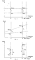
- phase variation for k1 and k2 with IF deviation is shown in principle in the phase/frequency diagram in Figure 1 (no frequency error in the sampling clock).
- the total phase shift between two OFDM frames for frequencies k1 and k2 consists of a part f which is the same for k1 and k2 and is proportional to the frequency translation.
- the function contains the sum of d 1 and d 2 which must be cancelled out. Utilize the known function F1 which only contains d 1 and d 2 .
- F2 (D k1 + D k2 ) - (D k1 - D k2 )C where C is a constant.
- the method according to the invention complements the method of this type of control.
- the method is based on detecting the absolute phase error for both synchronization symbols as distinct from the original method which is based on differential detection of phase errors of the symbols.
- absolute phase is meant the phase deviation from the known phase of k1 and k2.
- the phase is controlled with the IF clock whilst the timing error is controlled with the sampling clock.
- the frequencies are calculated according to the index in Figure 4.
- the frequency for index 1 in the OFDM frame corresponds to the direct-voltage component. This is followed by positive frequencies up to the Nyquist frequency minus one. The negative frequencies begin with index N and back in the OFDM frame to index N/2+1.
- index(k1) N- index(k2) + 2 where k1 represents the negative frequency.
- a timing error in the sampling of the baseband signal entails that the symbols (frequencies) are given a linear phase shift. Even if the sampling occurs at the right frequency, this must also occur at the right time for this linear phase shift not to occur.
- phase error before sampling entails a constant phase shift of all symbols (frequencies). This error remains after control of the frequency of the IF clock.
- phase shift is always linear for all combinations of both types of error, it is sufficient to study the phase shift for the two frequencies k1 and k2.
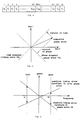
- the control method according to the invention is described most easily if we study the plane of complex numbers, the axes of which consist of the absolute phase error ⁇ 1 and ⁇ 2 for the symbols k1 and k2 (see Figure 5).
- the phase error will lie on the diagonal with the angle ⁇ /4 (time diagonal).
- a frequency error or a phase shift before sampling means that the error is located on the time diagonal.
- a correct phase before sampling means that a timing error is located on the diagonal with the angle 3 ⁇ /4 (phase diagonal).
- both time and phase errors exist which implies that the composite phase error will be located at an arbitrary location in the plane of complex numbers.
- the error therefore mainly consists of a positive or, respectively, negative phase error where phase control is mainly carried out.
- the error mainly consists of a negative or, respectively, positive timing error whereby time control is mainly carried out.
- phase error ⁇ 1 + ⁇ 2
- a negative phase shift of ⁇ /4 implies that the diagonals form new coordinate axes. This implies that the real and imaginary part of the error ⁇ forms error signals.
- phase error can also be read from the phase for frequency f 0 . This is logical since this frequency corresponds to the direct-voltage component in the FFT operation. If the phase error is zero before sampling, variations in the sampling frequency and time will not affect the phase of the direct-voltage component.
- OFDM is a digital complex modulation method where, generally speaking, all signal processing at the baseband is done by digital components of the types of signal processors, FFT processors and specific circuit solutions.
- the transmitted signal is analog which requires a number of analog components for processing the radio signal before conversion to or from the digital baseband representation. These analog components occur primarily in the up and down conversion of the signal to RF and IF, channel filtering and in sampling. A large proportion of the synchronization problems which arise originates from deviations and imperfections of these, which is why control of them is required.
- the digital representation of the baseband signal is read in by an FFT processor, by means of which the latter carries out conversion of the time signal to the frequency domain.
- the received symbols in the OFDM frame are now located at a respective frequency (point) which has been calculated by the FFT processor.
- the two known symbols are multiplexed out by a demultiplexer unit.
- the two known symbols k1 and k2 form the input signal to the unit for calculating the error signals F1 and F2.
- the errors are integrated via two digital integrators (PI control).
- the control method according to the invention is implemented according to Figure 10.
- Frequency control according to earlier techniques is found at the top left. This part however has been modified through choice of symmetrically chosen synchronization frequencies k1 and k2.
- Phase and time control is found on the right and in the frequency control part.
- the error signals F1 and F2 are the error signals which control the control of the sampling and, respectively, IF clock.
- F1 consists of the sum of the error of the sampling frequency and the timing error.
- F2 correspondingly consists of the sum of the error of the IF frequency and phase error.
- phase and timing errors Before adding the phase and timing errors to become F1 and F2, they must be scaled for the control to be balanced. Simulations show that a suitable scaling factor for phase and timing errors is 0.1. This choice of scaling factor means that the frequency control will be quicker than phase and time control.
- the error signals F1 and F2 are optimally updated continuously for each OFDM frame. This updating rate can be difficult to achieve in a broadband OFDM system due to the limited calculating capacity in the existing hardware. If the control signals are updated at an interval to a number of frames, this implies that a lower band width is required for the disturbances than with continuous control of each OFDM frame.
- the control method according to the invention including digital integrators includes the following calculation operations: 2 complex divisions, 4 arc-tan calculations, 8 real additions, 4 real multiplications and 4 delays (2 complex and 2 real).
Landscapes
- Engineering & Computer Science (AREA)
- Computer Networks & Wireless Communication (AREA)
- Signal Processing (AREA)
- Synchronisation In Digital Transmission Systems (AREA)
Claims (9)
- Verfahren für die Synchronisierung bei OFDM Modulation (orthogonales Frequenz-Multiplex), die in einem Empfänger durchgeführt wird, wobei Frequenzfehler in einem Zwischenfrequenztakt und einem Abtasttakt dadurch gesteuert werden, daß die Abweichung des Abtasttaktes und des Zwischenfrequenztaktes für zwei Unterträger mit unterschiedlichen Frequenzen (k1, k2) abgeschätzt wird, dadurch gekennzeichnet, daßdie Frequenzen der Unterträger (k1, k2) symmetrisch um Null gewählt werden,die absoluten Phasenfehler 1, 2 für beide Unterträger detektiert werden,ein Taktfehler und ein Phasenfehler von den absoluten Phasenfehlern 1, 2 gebildet werden,ein erstes Steuersignal (F1) von der Abweichung des Abtasttaktes und dem Taktfehler zum Steuern des Abtasttaktes gebildet wird, undein zweites Steuersignal (F2) von der Abweichung des Zwischenfrequenztaktes und dem Phasenfehler zum Steuern des Zwischenfrequenztaktes gebildet wird.
- Verfahren nach Anspruch 1, dadurch gekennzeichnet, daß der Taktfehler als die Differenz zwischen den absoluten Phasenfehlern 2-1 berechnet wird und der Phasenfehler als die Summe der absoluten Phasenfehler 1+2 berechnet wird.
- Verfahren nach Anspruch 1 oder 2, dadurch gekennzeichnet, daßdas erste Steuersignal durch die Summe der Abweichung des Abtasttaktes und des Taktfehlers gebildet wird, und daßdas zweite Steuersignal durch die Summe der Abweichung des Zwischenfrequenztaktes und des Phasenfehlers gebildet wird.
- Verfahren nach Anspruch 3, dadurch gekennzeichnet, daß der Taktfehler und der Phasenfehler durch einen geeigneten Maßstabsfaktor skaliert werden, bevor sie addiert werden, um entsprechende Steuersignale (F1, F2) zu bilden.
- Verfahren nach Anspruch 4, dadurch gekennzeichnet, daß der Maßstabsfaktor 0,1 beträgt.
- Verfahren nach einem der vorangehenden Ansprüche, dadurch gekennzeichnet, daß die Steuersignale für jeden OFDM-Datenblock aktualisiert werden.
- Anordnung zur Synchronisierung bei OFDM Modulation, die in einem Empfänger durchgeführt wird, die einen Abwärtswandler für Abwärtswandlung eines Zwischenfrequenzsignals auf Basisbandkomponenten, welcher Abwärtswandler durch einen Oszillator mit einem Zwischenfrequenztakt gesteuert wird, einen Analog-/Digitalwandler zum Digitalisieren der Basisbandkomponenten, welcher Analog-/Digitalwandler durch einen anderen Oszillator mit einem Abtasttakt gesteuert wird, einen FFT-Prozessor (schnelle Fourier-Transformation) zum Wandeln der Basisbandkomponenten von der Zeitdomäne zur Frequenzdomäne, eine Demultiplexiereinheit zum Bilden von zwei Unterträgern mit unterschiedlichen Frequenzen (k1, k2) aufweist, dadurch gekennzeichnet, daß die Demultiplexiereinheit dazu ausgebildet ist, die Frequenzen der Unterträger symmetrisch um Null herum auszuwählen, und durch Mittel zum Bilden der Abweichung des Abtasttaktes und des Zwischenfrequenztaktes, Mittel zum Bilden der absoluten Phasenfehler 1, 2 der beiden Unterträger, Mittel zum Bilden eines Taktfehlers und eines Phasenfehlers von den absoluten Phasenfehlern, Mittel zum Bilden eines ersten Steuersignales (F1) von der Abweichung des Abtasttaktes und dem Taktfehler zum Steuern des Abtasttaktes, und Mittel zum Bilden eines zweiten Steuersignales (F2) von der Abweichung des Zwischenfrequenztaktes und dem Phasenfehler zum Steuern des Zwischenfrequenztaktes.
- Anordnung nach Anspruch 7, dadurch gekennzeichnet, daß die Mittel zum Bilden der absoluten Phasenfehler eine Arcus-Tangens-Einheit einschließen, die Mittel zum Bilden des Taktfehlers eine Addiereinheit zum Bilden der Differenz zwischen den absoluten Phasenfehlern einschließen, die Mittel zum Bilden des Phasenfehlers eine Addiereinheit zum Bilden der Summe der absoluten Phasenfehler einschließen, und daß die Mittel zum Bilden der Steuersignale jeweils eine Addiereinheit zum Addieren der Abweichung des Abtasttaktes zum Taktfehler und der Abweichung des Zwischenfrequenztaktes zum Phasenfehler aufweisen.
- Anordnung nach Anspruch 8, gekennzeichnet durch Multipliziereinheiten zum Multiplizieren des Taktfehlers und des Phasenfehlers mit einem Maßstabsfaktor vor dem Addieren zu dem entsprechenden Steuersignal.
Applications Claiming Priority (3)
| Application Number | Priority Date | Filing Date | Title |
|---|---|---|---|
| SE9400116 | 1994-01-18 | ||
| SE9400116A SE501608C2 (sv) | 1994-01-18 | 1994-01-18 | Förfarande och arrangemang för synkronisering vid OFDM- modulering |
| PCT/SE1994/001266 WO1995019671A1 (en) | 1994-01-18 | 1994-12-30 | Method and arrangement for synchronization in ofdm modulation |
Publications (2)
| Publication Number | Publication Date |
|---|---|
| EP0740868A1 EP0740868A1 (de) | 1996-11-06 |
| EP0740868B1 true EP0740868B1 (de) | 2002-04-10 |
Family
ID=20392588
Family Applications (1)
| Application Number | Title | Priority Date | Filing Date |
|---|---|---|---|
| EP95907163A Expired - Lifetime EP0740868B1 (de) | 1994-01-18 | 1994-12-30 | Verfahren und einrichtung zur synchronisierung bei ofdm-modulation |
Country Status (6)
| Country | Link |
|---|---|
| US (1) | US5726973A (de) |
| EP (1) | EP0740868B1 (de) |
| DE (1) | DE69430387T2 (de) |
| DK (1) | DK0740868T3 (de) |
| SE (1) | SE501608C2 (de) |
| WO (1) | WO1995019671A1 (de) |
Families Citing this family (48)
| Publication number | Priority date | Publication date | Assignee | Title |
|---|---|---|---|---|
| US6334219B1 (en) | 1994-09-26 | 2001-12-25 | Adc Telecommunications Inc. | Channel selection for a hybrid fiber coax network |
| US5682376A (en) * | 1994-12-20 | 1997-10-28 | Matsushita Electric Industrial Co., Ltd. | Method of transmitting orthogonal frequency division multiplex signal, and transmitter and receiver employed therefor |
| USRE42236E1 (en) | 1995-02-06 | 2011-03-22 | Adc Telecommunications, Inc. | Multiuse subcarriers in multipoint-to-point communication using orthogonal frequency division multiplexing |
| US7280564B1 (en) | 1995-02-06 | 2007-10-09 | Adc Telecommunications, Inc. | Synchronization techniques in multipoint-to-point communication using orthgonal frequency division multiplexing |
| DE19534462C2 (de) * | 1995-09-16 | 1999-08-26 | Temic Semiconductor Gmbh | Übertragungsverfahren |
| JPH09130362A (ja) * | 1995-10-30 | 1997-05-16 | Sony Corp | 受信装置および受信方法 |
| US5802117A (en) * | 1996-02-08 | 1998-09-01 | Philips Electronics North America Corporation | Method and apparatus for joint frequency offset and timing estimation of a multicarrier modulation system |
| WO1997041672A1 (en) * | 1996-04-29 | 1997-11-06 | Philips Electronics N.V. | Symbol synchronisation in a multicarrier receiver |
| JP3511798B2 (ja) * | 1996-05-08 | 2004-03-29 | 三菱電機株式会社 | ディジタル放送受信機 |
| JPH09307526A (ja) * | 1996-05-17 | 1997-11-28 | Mitsubishi Electric Corp | デジタル放送受信機 |
| GB9614712D0 (en) * | 1996-07-12 | 1996-09-04 | Roke Manor Research | Improvements in or relating to radio receivers |
| KR100221336B1 (ko) * | 1996-12-28 | 1999-09-15 | 전주범 | 직교 주파수 분할 다중화 수신 시스템의 프레임 동기 장치 및 그 방법 |
| KR100230271B1 (ko) * | 1997-01-10 | 1999-11-15 | 윤종용 | Ofdm 시스템 수신기의 미세 fft 윈도우 위치 복원장치 |
| SE517930C2 (sv) | 1997-01-31 | 2002-08-06 | Ericsson Telefon Ab L M | Förfarande och anordning för initial synkronisering i ett kommunikationssystem |
| EP0859494A3 (de) * | 1997-02-17 | 2000-08-23 | Matsushita Electric Industrial Co., Ltd. | Synchronisierung vom lokalen Oszillator, in Mehrträgersystem |
| KR100238047B1 (ko) * | 1997-02-25 | 2000-01-15 | 윤종용 | 직교 주파수분할 다중화 전송시스템의 반송파 주파수 동기 방법 및 동기 장치 |
| SE9703629L (sv) * | 1997-03-03 | 1998-09-04 | Telia Ab | Förbättringar av, eller med avseende på, synkronisering |
| GB2326069B (en) * | 1997-05-02 | 2002-06-19 | Lsi Logic Corp | Demodulating digital video broadcast signals |
| JP3797397B2 (ja) | 1997-05-02 | 2006-07-19 | ソニー株式会社 | 受信装置および受信方法 |
| US5867478A (en) * | 1997-06-20 | 1999-02-02 | Motorola, Inc. | Synchronous coherent orthogonal frequency division multiplexing system, method, software and device |
| DE19733825A1 (de) * | 1997-08-05 | 1999-02-11 | Siemens Ag | Verfahren und Anordnung zur kombinierten Messung des Anfangs eines Datenblocks und des Trägerfrequenzversatzes in einem Mehrträgerübertragungssystem für unregelmäßige Übertragung von Datenblöcken |
| DE19742670B4 (de) * | 1997-09-26 | 2011-08-11 | Telefonaktiebolaget Lm Ericsson (Publ) | Verfahren, Empfänger und Mehrträger-QAM-System zur Demodulation eines analogen Mehrträger-QAM-Signals |
| US6618352B1 (en) | 1998-05-26 | 2003-09-09 | Matsushita Electric Industrial Co., Ltd. | Modulator, demodulator, and transmission system for use in OFDM transmission |
| US6310926B1 (en) | 1998-09-25 | 2001-10-30 | Telefonaktiebolaget Lm Ericsson (Publ) | Adjustment of the sampling frequency in a multicarrier receiver |
| US6111919A (en) * | 1999-01-20 | 2000-08-29 | Intellon Corporation | Synchronization of OFDM signals |
| EP1028564B1 (de) | 1999-02-11 | 2010-04-07 | Motorola, Inc. | Schätzung von Träger- und Abtastungsfrequenzverschiebungen in Mehrträgerempfängern |
| FR2790344B1 (fr) * | 1999-02-26 | 2001-05-18 | St Microelectronics Sa | Demodulateur cofdm avec compensation de deplacement de fenetre d'analyse fft |
| US6074086A (en) * | 1999-04-26 | 2000-06-13 | Intellon Corporation | Synchronization of OFDM signals with improved windowing |
| US6269132B1 (en) | 1999-04-26 | 2001-07-31 | Intellon Corporation | Windowing function for maintaining orthogonality of channels in the reception of OFDM symbols |
| US6505037B1 (en) * | 1999-06-29 | 2003-01-07 | Sharp Laboratories Of America, Inc. | Data unit detection including antenna diversity |
| US6859504B1 (en) | 1999-06-29 | 2005-02-22 | Sharp Laboratories Of America, Inc. | Rapid settling automatic gain control with minimal signal distortion |
| US6631143B1 (en) * | 1999-11-12 | 2003-10-07 | Lucent Technologies Inc. | Methods and apparatus for frame synchronization in a digital audio broadcasting system |
| US7020074B1 (en) * | 2000-04-03 | 2006-03-28 | Nortel Networks Limited | Synchronization method and apparatus for frequency division multiplexed telecommunication systems |
| CA2352398C (en) * | 2000-07-06 | 2005-07-26 | Unique Broadband Systems, Inc. | Low phase noise frequency converter |
| US7177372B2 (en) * | 2000-12-21 | 2007-02-13 | Jian Gu | Method and apparatus to remove effects of I-Q imbalances of quadrature modulators and demodulators in a multi-carrier system |
| FR2821216B1 (fr) * | 2001-02-20 | 2003-10-24 | Sagem | Procede de synchronisation d'un signal d'horloge avec un signal de reference |
| US7218691B1 (en) | 2001-03-05 | 2007-05-15 | Marvell International Ltd. | Method and apparatus for estimation of orthogonal frequency division multiplexing symbol timing and carrier frequency offset |
| US8619922B1 (en) | 2002-02-04 | 2013-12-31 | Marvell International Ltd. | Method and apparatus for acquisition and tracking of orthogonal frequency division multiplexing symbol timing, carrier frequency offset and phase noise |
| DE10208650A1 (de) * | 2001-03-15 | 2002-09-19 | Bosch Gmbh Robert | Verfahren und Vorrichtung zur Synchronisation wenigstens eines Teilnehmers eines Bussystems und Bussystem |
| AU2002316435B2 (en) | 2001-06-27 | 2008-02-21 | Skky, Llc | Improved media delivery platform |
| KR100441501B1 (ko) * | 2002-01-17 | 2004-07-23 | 삼성전자주식회사 | 오에프디엠수신기의 심볼 타이밍 복원장치 및 방법 |
| KR100406975B1 (ko) * | 2002-01-29 | 2003-11-28 | 삼성전자주식회사 | 오에프디엠수신기의 심볼 타이밍 복원장치 및 방법 |
| US7020226B1 (en) * | 2002-04-04 | 2006-03-28 | Nortel Networks Limited | I/Q distortion compensation for the reception of OFDM signals |
| US7224666B2 (en) | 2002-05-13 | 2007-05-29 | Texas Instruments Incorporated | Estimating frequency offsets using pilot tones in an OFDM system |
| KR100500404B1 (ko) * | 2002-11-06 | 2005-07-12 | (주)실리콘바인 | 샘플링 클럭 복원을 위한 클럭 오차 검출 방법과 그 방법을 채용한 오에프디엠 수신기 |
| JP2005197968A (ja) * | 2004-01-06 | 2005-07-21 | Fujitsu Ltd | 信号処理回路並びに直交復調装置およびその誤差推定方法 |
| TW201141144A (en) * | 2009-11-16 | 2011-11-16 | Maxlinear Inc | Apparatus and methods for symbol timing error detection, tracking and correction |
| US10944535B2 (en) | 2019-05-29 | 2021-03-09 | Shure Acquisition Holdings, Inc. | OFDMA baseband clock synchronization |
Family Cites Families (5)
| Publication number | Priority date | Publication date | Assignee | Title |
|---|---|---|---|---|
| GB9020170D0 (en) * | 1990-09-14 | 1990-10-24 | Indep Broadcasting Authority | Orthogonal frequency division multiplexing |
| US5206886A (en) * | 1990-04-16 | 1993-04-27 | Telebit Corporation | Method and apparatus for correcting for clock and carrier frequency offset, and phase jitter in mulicarrier modems |
| FR2670062B1 (fr) * | 1990-11-30 | 1993-11-12 | Thomson Csf | Procede de recalage des oscillateurs locaux d'un recepteur et dispositif pour la mise en óoeuvre du procede. |
| JP3041175B2 (ja) * | 1993-11-12 | 2000-05-15 | 株式会社東芝 | Ofdm同期復調回路 |
| JP3074103B2 (ja) * | 1993-11-16 | 2000-08-07 | 株式会社東芝 | Ofdm同期復調回路 |
-
1994
- 1994-01-18 SE SE9400116A patent/SE501608C2/sv not_active IP Right Cessation
- 1994-12-30 WO PCT/SE1994/001266 patent/WO1995019671A1/en not_active Ceased
- 1994-12-30 EP EP95907163A patent/EP0740868B1/de not_active Expired - Lifetime
- 1994-12-30 US US08/669,379 patent/US5726973A/en not_active Expired - Lifetime
- 1994-12-30 DE DE69430387T patent/DE69430387T2/de not_active Expired - Lifetime
- 1994-12-30 DK DK95907163T patent/DK0740868T3/da active
Also Published As
| Publication number | Publication date |
|---|---|
| DK0740868T3 (da) | 2002-07-22 |
| SE9400116L (sv) | 1995-03-27 |
| EP0740868A1 (de) | 1996-11-06 |
| US5726973A (en) | 1998-03-10 |
| WO1995019671A1 (en) | 1995-07-20 |
| SE501608C2 (sv) | 1995-03-27 |
| SE9400116D0 (sv) | 1994-01-18 |
| DE69430387D1 (de) | 2002-05-16 |
| DE69430387T2 (de) | 2002-12-12 |
Similar Documents
| Publication | Publication Date | Title |
|---|---|---|
| EP0740868B1 (de) | Verfahren und einrichtung zur synchronisierung bei ofdm-modulation | |
| EP0573541B1 (de) | System für Sendung und Empfang von digitalen Daten, Empfänger und Sender zur Verwendung in einem solchen System | |
| US5602835A (en) | OFDM synchronization demodulation circuit | |
| US7453792B2 (en) | Receiver architecture for pilot based OFDM systems | |
| US6304545B1 (en) | Method and circuit arrangement for the correction of phase and/or frequency errors in digital multicarrier signals | |
| US5263196A (en) | Method and apparatus for compensation of imbalance in zero-if downconverters | |
| US5268647A (en) | Method and arrangement of coherently demodulating PSK signals using a feedback loop including a filter bank | |
| US8976914B2 (en) | Multi-tap IQ imbalance estimation and correction circuit and method | |
| JPH10294713A (ja) | 直交周波数分割多重化伝送システムの搬送波周波数同期方法及び同期装置 | |
| JP3058870B1 (ja) | Afc回路 | |
| JP2000278237A (ja) | Ofdm用中継装置 | |
| JP3576420B2 (ja) | 周波数オフセット補正装置 | |
| US6204726B1 (en) | Digital demodulator | |
| KR100809206B1 (ko) | 직교 주파수 분할 다중 수신기의 시간영역 iq 부정합검출 장치 | |
| US6553066B1 (en) | Time error compensation arrangement and multi-carrier modem comprising the arrangement | |
| EP1039715A1 (de) | Zwischenverstärker eines OFDM-Übertragungssignals | |
| GB2365283A (en) | Multi-carrier signal and transmission and reception thereof | |
| JP3148090B2 (ja) | Ofdm信号同期復調器 | |
| JP3751385B2 (ja) | 信号復調装置 | |
| EP0818904A2 (de) | Taktrückgewinnung für DAB-Empfänger | |
| JPH10257117A (ja) | 受信デジタル信号の搬送周波数と受信局部発振器の周波数との間の周波数差を推定する装置、および対応する受信機 | |
| JP3549957B2 (ja) | 自動周波数制御方法および装置 | |
| JP2000278241A (ja) | Ofdm用中継装置 | |
| JPH10276166A (ja) | Afc回路 | |
| KR100493269B1 (ko) | 디지털티브이의자동주파수제어장치 |
Legal Events
| Date | Code | Title | Description |
|---|---|---|---|
| PUAI | Public reference made under article 153(3) epc to a published international application that has entered the european phase |
Free format text: ORIGINAL CODE: 0009012 |
|
| 17P | Request for examination filed |
Effective date: 19960709 |
|
| AK | Designated contracting states |
Kind code of ref document: A1 Designated state(s): CH DE DK ES FR GB IT LI NL |
|
| 17Q | First examination report despatched |
Effective date: 20000803 |
|
| GRAG | Despatch of communication of intention to grant |
Free format text: ORIGINAL CODE: EPIDOS AGRA |
|
| RIC1 | Information provided on ipc code assigned before grant |
Free format text: 7H 04L 5/06 A, 7H 04L 27/26 B |
|
| GRAG | Despatch of communication of intention to grant |
Free format text: ORIGINAL CODE: EPIDOS AGRA |
|
| GRAH | Despatch of communication of intention to grant a patent |
Free format text: ORIGINAL CODE: EPIDOS IGRA |
|
| REG | Reference to a national code |
Ref country code: GB Ref legal event code: IF02 |
|
| GRAH | Despatch of communication of intention to grant a patent |
Free format text: ORIGINAL CODE: EPIDOS IGRA |
|
| GRAA | (expected) grant |
Free format text: ORIGINAL CODE: 0009210 |
|
| RIN1 | Information on inventor provided before grant (corrected) |
Inventor name: ISAKSSON, MIKAEL |
|
| AK | Designated contracting states |
Kind code of ref document: B1 Designated state(s): CH DE DK ES FR GB IT LI NL |
|
| PG25 | Lapsed in a contracting state [announced via postgrant information from national office to epo] |
Ref country code: NL Free format text: LAPSE BECAUSE OF FAILURE TO SUBMIT A TRANSLATION OF THE DESCRIPTION OR TO PAY THE FEE WITHIN THE PRESCRIBED TIME-LIMIT Effective date: 20020410 Ref country code: LI Free format text: LAPSE BECAUSE OF FAILURE TO SUBMIT A TRANSLATION OF THE DESCRIPTION OR TO PAY THE FEE WITHIN THE PRESCRIBED TIME-LIMIT Effective date: 20020410 Ref country code: IT Free format text: LAPSE BECAUSE OF FAILURE TO SUBMIT A TRANSLATION OF THE DESCRIPTION OR TO PAY THE FEE WITHIN THE PRESCRIBED TIME-LIMIT;WARNING: LAPSES OF ITALIAN PATENTS WITH EFFECTIVE DATE BEFORE 2007 MAY HAVE OCCURRED AT ANY TIME BEFORE 2007. THE CORRECT EFFECTIVE DATE MAY BE DIFFERENT FROM THE ONE RECORDED. Effective date: 20020410 Ref country code: CH Free format text: LAPSE BECAUSE OF FAILURE TO SUBMIT A TRANSLATION OF THE DESCRIPTION OR TO PAY THE FEE WITHIN THE PRESCRIBED TIME-LIMIT Effective date: 20020410 |
|
| REG | Reference to a national code |
Ref country code: CH Ref legal event code: EP |
|
| REF | Corresponds to: |
Ref document number: 69430387 Country of ref document: DE Date of ref document: 20020516 |
|
| REG | Reference to a national code |
Ref country code: DK Ref legal event code: T3 |
|
| NLV1 | Nl: lapsed or annulled due to failure to fulfill the requirements of art. 29p and 29m of the patents act | ||
| ET | Fr: translation filed | ||
| REG | Reference to a national code |
Ref country code: CH Ref legal event code: PL |
|
| PG25 | Lapsed in a contracting state [announced via postgrant information from national office to epo] |
Ref country code: ES Free format text: LAPSE BECAUSE OF FAILURE TO SUBMIT A TRANSLATION OF THE DESCRIPTION OR TO PAY THE FEE WITHIN THE PRESCRIBED TIME-LIMIT Effective date: 20021030 |
|
| PLBE | No opposition filed within time limit |
Free format text: ORIGINAL CODE: 0009261 |
|
| STAA | Information on the status of an ep patent application or granted ep patent |
Free format text: STATUS: NO OPPOSITION FILED WITHIN TIME LIMIT |
|
| 26N | No opposition filed |
Effective date: 20030113 |
|
| PGFP | Annual fee paid to national office [announced via postgrant information from national office to epo] |
Ref country code: DK Payment date: 20131219 Year of fee payment: 20 Ref country code: DE Payment date: 20131220 Year of fee payment: 20 Ref country code: GB Payment date: 20131219 Year of fee payment: 20 |
|
| PGFP | Annual fee paid to national office [announced via postgrant information from national office to epo] |
Ref country code: FR Payment date: 20131220 Year of fee payment: 20 |
|
| REG | Reference to a national code |
Ref country code: DE Ref legal event code: R071 Ref document number: 69430387 Country of ref document: DE |
|
| REG | Reference to a national code |
Ref country code: DE Ref legal event code: R071 Ref document number: 69430387 Country of ref document: DE |
|
| REG | Reference to a national code |
Ref country code: DK Ref legal event code: EUP Effective date: 20141230 |
|
| REG | Reference to a national code |
Ref country code: GB Ref legal event code: PE20 Expiry date: 20141229 |
|
| PG25 | Lapsed in a contracting state [announced via postgrant information from national office to epo] |
Ref country code: GB Free format text: LAPSE BECAUSE OF EXPIRATION OF PROTECTION Effective date: 20141229 |