EP0987931A2 - Verbundfolie aus Aluminium und Kupfer - Google Patents
Verbundfolie aus Aluminium und Kupfer Download PDFInfo
- Publication number
- EP0987931A2 EP0987931A2 EP99306233A EP99306233A EP0987931A2 EP 0987931 A2 EP0987931 A2 EP 0987931A2 EP 99306233 A EP99306233 A EP 99306233A EP 99306233 A EP99306233 A EP 99306233A EP 0987931 A2 EP0987931 A2 EP 0987931A2
- Authority
- EP
- European Patent Office
- Prior art keywords
- layer
- copper
- ultra
- foil
- zinc
- Prior art date
- Legal status (The legal status is an assumption and is not a legal conclusion. Google has not performed a legal analysis and makes no representation as to the accuracy of the status listed.)
- Withdrawn
Links
Images

Classifications
-
- H—ELECTRICITY
- H05—ELECTRIC TECHNIQUES NOT OTHERWISE PROVIDED FOR
- H05K—PRINTED CIRCUITS; CASINGS OR CONSTRUCTIONAL DETAILS OF ELECTRIC APPARATUS; MANUFACTURE OF ASSEMBLAGES OF ELECTRICAL COMPONENTS
- H05K3/00—Apparatus or processes for manufacturing printed circuits
- H05K3/02—Apparatus or processes for manufacturing printed circuits in which the conductive material is applied to the surface of the insulating support and is thereafter removed from such areas of the surface which are not intended for current conducting or shielding
- H05K3/022—Processes for manufacturing precursors of printed circuits, i.e. copper-clad substrates
- H05K3/025—Processes for manufacturing precursors of printed circuits, i.e. copper-clad substrates by transfer of thin metal foil formed on a temporary carrier, e.g. peel-apart copper
-
- H—ELECTRICITY
- H05—ELECTRIC TECHNIQUES NOT OTHERWISE PROVIDED FOR
- H05K—PRINTED CIRCUITS; CASINGS OR CONSTRUCTIONAL DETAILS OF ELECTRIC APPARATUS; MANUFACTURE OF ASSEMBLAGES OF ELECTRICAL COMPONENTS
- H05K3/00—Apparatus or processes for manufacturing printed circuits
-
- C—CHEMISTRY; METALLURGY
- C25—ELECTROLYTIC OR ELECTROPHORETIC PROCESSES; APPARATUS THEREFOR
- C25D—PROCESSES FOR THE ELECTROLYTIC OR ELECTROPHORETIC PRODUCTION OF COATINGS; ELECTROFORMING; APPARATUS THEREFOR
- C25D1/00—Electroforming
- C25D1/04—Wires; Strips; Foils
-
- C—CHEMISTRY; METALLURGY
- C25—ELECTROLYTIC OR ELECTROPHORETIC PROCESSES; APPARATUS THEREFOR
- C25D—PROCESSES FOR THE ELECTROLYTIC OR ELECTROPHORETIC PRODUCTION OF COATINGS; ELECTROFORMING; APPARATUS THEREFOR
- C25D5/00—Electroplating characterised by the process; Pretreatment or after-treatment of workpieces
- C25D5/10—Electroplating with more than one layer of the same or of different metals
-
- C—CHEMISTRY; METALLURGY
- C25—ELECTROLYTIC OR ELECTROPHORETIC PROCESSES; APPARATUS THEREFOR
- C25D—PROCESSES FOR THE ELECTROLYTIC OR ELECTROPHORETIC PRODUCTION OF COATINGS; ELECTROFORMING; APPARATUS THEREFOR
- C25D5/00—Electroplating characterised by the process; Pretreatment or after-treatment of workpieces
- C25D5/60—Electroplating characterised by the structure or texture of the layers
- C25D5/605—Surface topography of the layers, e.g. rough, dendritic or nodular layers
-
- C—CHEMISTRY; METALLURGY
- C25—ELECTROLYTIC OR ELECTROPHORETIC PROCESSES; APPARATUS THEREFOR
- C25D—PROCESSES FOR THE ELECTROLYTIC OR ELECTROPHORETIC PRODUCTION OF COATINGS; ELECTROFORMING; APPARATUS THEREFOR
- C25D5/00—Electroplating characterised by the process; Pretreatment or after-treatment of workpieces
- C25D5/60—Electroplating characterised by the structure or texture of the layers
- C25D5/623—Porosity of the layers
-
- Y—GENERAL TAGGING OF NEW TECHNOLOGICAL DEVELOPMENTS; GENERAL TAGGING OF CROSS-SECTIONAL TECHNOLOGIES SPANNING OVER SEVERAL SECTIONS OF THE IPC; TECHNICAL SUBJECTS COVERED BY FORMER USPC CROSS-REFERENCE ART COLLECTIONS [XRACs] AND DIGESTS
- Y10—TECHNICAL SUBJECTS COVERED BY FORMER USPC
- Y10S—TECHNICAL SUBJECTS COVERED BY FORMER USPC CROSS-REFERENCE ART COLLECTIONS [XRACs] AND DIGESTS
- Y10S428/00—Stock material or miscellaneous articles
- Y10S428/901—Printed circuit
-
- Y—GENERAL TAGGING OF NEW TECHNOLOGICAL DEVELOPMENTS; GENERAL TAGGING OF CROSS-SECTIONAL TECHNOLOGIES SPANNING OVER SEVERAL SECTIONS OF THE IPC; TECHNICAL SUBJECTS COVERED BY FORMER USPC CROSS-REFERENCE ART COLLECTIONS [XRACs] AND DIGESTS
- Y10—TECHNICAL SUBJECTS COVERED BY FORMER USPC
- Y10S—TECHNICAL SUBJECTS COVERED BY FORMER USPC CROSS-REFERENCE ART COLLECTIONS [XRACs] AND DIGESTS
- Y10S428/00—Stock material or miscellaneous articles
- Y10S428/922—Static electricity metal bleed-off metallic stock
- Y10S428/923—Physical dimension
- Y10S428/924—Composite
- Y10S428/926—Thickness of individual layer specified
-
- Y—GENERAL TAGGING OF NEW TECHNOLOGICAL DEVELOPMENTS; GENERAL TAGGING OF CROSS-SECTIONAL TECHNOLOGIES SPANNING OVER SEVERAL SECTIONS OF THE IPC; TECHNICAL SUBJECTS COVERED BY FORMER USPC CROSS-REFERENCE ART COLLECTIONS [XRACs] AND DIGESTS
- Y10—TECHNICAL SUBJECTS COVERED BY FORMER USPC
- Y10S—TECHNICAL SUBJECTS COVERED BY FORMER USPC CROSS-REFERENCE ART COLLECTIONS [XRACs] AND DIGESTS
- Y10S428/00—Stock material or miscellaneous articles
- Y10S428/922—Static electricity metal bleed-off metallic stock
- Y10S428/9335—Product by special process
- Y10S428/934—Electrical process
- Y10S428/935—Electroplating
-
- Y—GENERAL TAGGING OF NEW TECHNOLOGICAL DEVELOPMENTS; GENERAL TAGGING OF CROSS-SECTIONAL TECHNOLOGIES SPANNING OVER SEVERAL SECTIONS OF THE IPC; TECHNICAL SUBJECTS COVERED BY FORMER USPC CROSS-REFERENCE ART COLLECTIONS [XRACs] AND DIGESTS
- Y10—TECHNICAL SUBJECTS COVERED BY FORMER USPC
- Y10T—TECHNICAL SUBJECTS COVERED BY FORMER US CLASSIFICATION
- Y10T156/00—Adhesive bonding and miscellaneous chemical manufacture
- Y10T156/11—Methods of delaminating, per se; i.e., separating at bonding face
-
- Y—GENERAL TAGGING OF NEW TECHNOLOGICAL DEVELOPMENTS; GENERAL TAGGING OF CROSS-SECTIONAL TECHNOLOGIES SPANNING OVER SEVERAL SECTIONS OF THE IPC; TECHNICAL SUBJECTS COVERED BY FORMER USPC CROSS-REFERENCE ART COLLECTIONS [XRACs] AND DIGESTS
- Y10—TECHNICAL SUBJECTS COVERED BY FORMER USPC
- Y10T—TECHNICAL SUBJECTS COVERED BY FORMER US CLASSIFICATION
- Y10T428/00—Stock material or miscellaneous articles
- Y10T428/12—All metal or with adjacent metals
- Y10T428/12431—Foil or filament smaller than 6 mils
- Y10T428/12438—Composite
-
- Y—GENERAL TAGGING OF NEW TECHNOLOGICAL DEVELOPMENTS; GENERAL TAGGING OF CROSS-SECTIONAL TECHNOLOGIES SPANNING OVER SEVERAL SECTIONS OF THE IPC; TECHNICAL SUBJECTS COVERED BY FORMER USPC CROSS-REFERENCE ART COLLECTIONS [XRACs] AND DIGESTS
- Y10—TECHNICAL SUBJECTS COVERED BY FORMER USPC
- Y10T—TECHNICAL SUBJECTS COVERED BY FORMER US CLASSIFICATION
- Y10T428/00—Stock material or miscellaneous articles
- Y10T428/12—All metal or with adjacent metals
- Y10T428/12479—Porous [e.g., foamed, spongy, cracked, etc.]
-
- Y—GENERAL TAGGING OF NEW TECHNOLOGICAL DEVELOPMENTS; GENERAL TAGGING OF CROSS-SECTIONAL TECHNOLOGIES SPANNING OVER SEVERAL SECTIONS OF THE IPC; TECHNICAL SUBJECTS COVERED BY FORMER USPC CROSS-REFERENCE ART COLLECTIONS [XRACs] AND DIGESTS
- Y10—TECHNICAL SUBJECTS COVERED BY FORMER USPC
- Y10T—TECHNICAL SUBJECTS COVERED BY FORMER US CLASSIFICATION
- Y10T428/00—Stock material or miscellaneous articles
- Y10T428/12—All metal or with adjacent metals
- Y10T428/12493—Composite; i.e., plural, adjacent, spatially distinct metal components [e.g., layers, joint, etc.]
- Y10T428/12639—Adjacent, identical composition, components
- Y10T428/12646—Group VIII or IB metal-base
-
- Y—GENERAL TAGGING OF NEW TECHNOLOGICAL DEVELOPMENTS; GENERAL TAGGING OF CROSS-SECTIONAL TECHNOLOGIES SPANNING OVER SEVERAL SECTIONS OF THE IPC; TECHNICAL SUBJECTS COVERED BY FORMER USPC CROSS-REFERENCE ART COLLECTIONS [XRACs] AND DIGESTS
- Y10—TECHNICAL SUBJECTS COVERED BY FORMER USPC
- Y10T—TECHNICAL SUBJECTS COVERED BY FORMER US CLASSIFICATION
- Y10T428/00—Stock material or miscellaneous articles
- Y10T428/12—All metal or with adjacent metals
- Y10T428/12493—Composite; i.e., plural, adjacent, spatially distinct metal components [e.g., layers, joint, etc.]
- Y10T428/12708—Sn-base component
- Y10T428/12715—Next to Group IB metal-base component
-
- Y—GENERAL TAGGING OF NEW TECHNOLOGICAL DEVELOPMENTS; GENERAL TAGGING OF CROSS-SECTIONAL TECHNOLOGIES SPANNING OVER SEVERAL SECTIONS OF THE IPC; TECHNICAL SUBJECTS COVERED BY FORMER USPC CROSS-REFERENCE ART COLLECTIONS [XRACs] AND DIGESTS
- Y10—TECHNICAL SUBJECTS COVERED BY FORMER USPC
- Y10T—TECHNICAL SUBJECTS COVERED BY FORMER US CLASSIFICATION
- Y10T428/00—Stock material or miscellaneous articles
- Y10T428/12—All metal or with adjacent metals
- Y10T428/12493—Composite; i.e., plural, adjacent, spatially distinct metal components [e.g., layers, joint, etc.]
- Y10T428/12736—Al-base component
- Y10T428/1275—Next to Group VIII or IB metal-base component
-
- Y—GENERAL TAGGING OF NEW TECHNOLOGICAL DEVELOPMENTS; GENERAL TAGGING OF CROSS-SECTIONAL TECHNOLOGIES SPANNING OVER SEVERAL SECTIONS OF THE IPC; TECHNICAL SUBJECTS COVERED BY FORMER USPC CROSS-REFERENCE ART COLLECTIONS [XRACs] AND DIGESTS
- Y10—TECHNICAL SUBJECTS COVERED BY FORMER USPC
- Y10T—TECHNICAL SUBJECTS COVERED BY FORMER US CLASSIFICATION
- Y10T428/00—Stock material or miscellaneous articles
- Y10T428/12—All metal or with adjacent metals
- Y10T428/12493—Composite; i.e., plural, adjacent, spatially distinct metal components [e.g., layers, joint, etc.]
- Y10T428/12771—Transition metal-base component
- Y10T428/12785—Group IIB metal-base component
- Y10T428/12792—Zn-base component
-
- Y—GENERAL TAGGING OF NEW TECHNOLOGICAL DEVELOPMENTS; GENERAL TAGGING OF CROSS-SECTIONAL TECHNOLOGIES SPANNING OVER SEVERAL SECTIONS OF THE IPC; TECHNICAL SUBJECTS COVERED BY FORMER USPC CROSS-REFERENCE ART COLLECTIONS [XRACs] AND DIGESTS
- Y10—TECHNICAL SUBJECTS COVERED BY FORMER USPC
- Y10T—TECHNICAL SUBJECTS COVERED BY FORMER US CLASSIFICATION
- Y10T428/00—Stock material or miscellaneous articles
- Y10T428/12—All metal or with adjacent metals
- Y10T428/12493—Composite; i.e., plural, adjacent, spatially distinct metal components [e.g., layers, joint, etc.]
- Y10T428/12771—Transition metal-base component
- Y10T428/12806—Refractory [Group IVB, VB, or VIB] metal-base component
- Y10T428/12826—Group VIB metal-base component
- Y10T428/12847—Cr-base component
-
- Y—GENERAL TAGGING OF NEW TECHNOLOGICAL DEVELOPMENTS; GENERAL TAGGING OF CROSS-SECTIONAL TECHNOLOGIES SPANNING OVER SEVERAL SECTIONS OF THE IPC; TECHNICAL SUBJECTS COVERED BY FORMER USPC CROSS-REFERENCE ART COLLECTIONS [XRACs] AND DIGESTS
- Y10—TECHNICAL SUBJECTS COVERED BY FORMER USPC
- Y10T—TECHNICAL SUBJECTS COVERED BY FORMER US CLASSIFICATION
- Y10T428/00—Stock material or miscellaneous articles
- Y10T428/12—All metal or with adjacent metals
- Y10T428/12493—Composite; i.e., plural, adjacent, spatially distinct metal components [e.g., layers, joint, etc.]
- Y10T428/12771—Transition metal-base component
- Y10T428/12861—Group VIII or IB metal-base component
- Y10T428/12903—Cu-base component
- Y10T428/1291—Next to Co-, Cu-, or Ni-base component
-
- Y—GENERAL TAGGING OF NEW TECHNOLOGICAL DEVELOPMENTS; GENERAL TAGGING OF CROSS-SECTIONAL TECHNOLOGIES SPANNING OVER SEVERAL SECTIONS OF THE IPC; TECHNICAL SUBJECTS COVERED BY FORMER USPC CROSS-REFERENCE ART COLLECTIONS [XRACs] AND DIGESTS
- Y10—TECHNICAL SUBJECTS COVERED BY FORMER USPC
- Y10T—TECHNICAL SUBJECTS COVERED BY FORMER US CLASSIFICATION
- Y10T428/00—Stock material or miscellaneous articles
- Y10T428/12—All metal or with adjacent metals
- Y10T428/12493—Composite; i.e., plural, adjacent, spatially distinct metal components [e.g., layers, joint, etc.]
- Y10T428/12771—Transition metal-base component
- Y10T428/12861—Group VIII or IB metal-base component
- Y10T428/12931—Co-, Fe-, or Ni-base components, alternative to each other
-
- Y—GENERAL TAGGING OF NEW TECHNOLOGICAL DEVELOPMENTS; GENERAL TAGGING OF CROSS-SECTIONAL TECHNOLOGIES SPANNING OVER SEVERAL SECTIONS OF THE IPC; TECHNICAL SUBJECTS COVERED BY FORMER USPC CROSS-REFERENCE ART COLLECTIONS [XRACs] AND DIGESTS
- Y10—TECHNICAL SUBJECTS COVERED BY FORMER USPC
- Y10T—TECHNICAL SUBJECTS COVERED BY FORMER US CLASSIFICATION
- Y10T428/00—Stock material or miscellaneous articles
- Y10T428/12—All metal or with adjacent metals
- Y10T428/12493—Composite; i.e., plural, adjacent, spatially distinct metal components [e.g., layers, joint, etc.]
- Y10T428/12771—Transition metal-base component
- Y10T428/12861—Group VIII or IB metal-base component
- Y10T428/12944—Ni-base component
-
- Y—GENERAL TAGGING OF NEW TECHNOLOGICAL DEVELOPMENTS; GENERAL TAGGING OF CROSS-SECTIONAL TECHNOLOGIES SPANNING OVER SEVERAL SECTIONS OF THE IPC; TECHNICAL SUBJECTS COVERED BY FORMER USPC CROSS-REFERENCE ART COLLECTIONS [XRACs] AND DIGESTS
- Y10—TECHNICAL SUBJECTS COVERED BY FORMER USPC
- Y10T—TECHNICAL SUBJECTS COVERED BY FORMER US CLASSIFICATION
- Y10T428/00—Stock material or miscellaneous articles
- Y10T428/31504—Composite [nonstructural laminate]
- Y10T428/31678—Of metal
Definitions
- the present invention relates generally to making and using ultra-thin copper foil and, more particularly, to a composite foil which facilitates handling of ultra-thin copper foil in the production of printed wiring boards.
- the invention also relates to a composite foil in which a unique metallic layer is disposed between an aluminum carrier and an ultra-thin copper foil, and the processes of producing and using such a composite foil.
- the copper foil used for making the circuit lines has tended to become thinner, for example, 12 ⁇ m thick foils are used, rather than conventional 35 ⁇ m and 18 ⁇ m foils.
- the need for thin copper foil has increased and ultra-thin copper foils have been tried. Handling a copper foil of 12 ⁇ m or less, however, is difficult. For example, it can wrinkle or tear while being produced and/or handled. Similar problems occur when an ultra-thin copper foil is used as the outer layer of a multi-layer printed wiring board. A method of preventing these problems with handling ultra-thin copper foil is needed.
- Printed wiring boards can be made from such supported ultra-thin copper foils by depositing a copper layer having a thickness of 1-12 ⁇ m onto a metal carrier layer having a thickness of 18-70 ⁇ m, then applying the exposed surface of the copper layer to a prepreg, such as a glass-reinforced epoxy resin or the like, and laminating by hot pressing. Finally, the metal carrier layer is separated, leaving a copper-clad laminate from which a printed wiring board can be made.
- a prepreg such as a glass-reinforced epoxy resin or the like
- the release layer is not uniform over the surface of the carrier layer, bond strength between the carrier layer and the ultra-thin copper foil is uneven. Consequently, when the carrier layer is peeled off after laminating a composite foil, if the bond strength is high, some of the ultra-thin copper foil may remain on the carrier layer and the required circuit pattern cannot be made. If the bond strength is weak, the ultra-thin copper foil may separate from the carrier layer prematurely during production and use of the composite foil.
- oxides, sulfides, metals, metal alloys or inorganic materials such as chromium or the like
- some of the inorganic material remains on the surface of the ultra-thin copper foil after the carrier layer is peeled off.
- the present inventors sought a composite foil which overcomes the problems discussed above and a process for making such composite foils. They investigated the metals and/or metal compounds which have conventionally been suggested as release layers for composite foils in the prior art.
- the inventors have found that deposition of copper directly on an aluminum surface, or one covered by aluminum oxide, is unsatisfactory since the bond strength is too weak. Consequently, the ultra-thin copper foil may easily be separated from an aluminum carrier during handling or laminating to insulating substrates.
- Zinc ions provided by a zinc compound in solution are contacted with the aluminum carrier.
- the aluminum surface is dissolved and replaced with zinc metal. It is possible to deposit ample zinc metal in a very short time. Thus, the zincate process is convenient, although not easily controlled. Electrodeposition of zinc is more readily controlled. But even with electrodeposition, the adhesion of zinc to aluminum is too strong to permit easy removal of the aluminum carrier.
- bond strength refers to the force required to separate the carrier layer from the ultra-thin copper foil.
- peel strength refers to the force required to separate the ultra-thin copper foil from a substrate to which it has been laminated.
- a composite foil of the invention comprises an aluminum carrier layer and an ultra-thin copper foil having a zinc-containing protective layer disposed between them.
- the protective layer consists of a porous layer of copper with interpenetrating zinc.
- the bond strength is sufficient to permit handling of the composite foil, but low enough to permit easy separation of the aluminum carrier from the ultra-thin copper foil after the latter has been laminated to an insulating substrate.
- the zinc is believed to provide needed bond strength, but it also provides protection for the ultra-thin copper foil after the aluminum carrier has been removed, thus exposing the copper.
- the protective layer comprises a porous layer of electrodeposited copper of about 500-4000 mg/m 2 of said aluminum carrier, preferably about 500-3000 mg/m 2 .
- the interpenetrating zinc is electrodeposited on the porous layer of copper.
- the amount of zinc deposited is preferably about 15-150 mg/m 2 of the aluminum carrier, more preferably about 50-100 mg/m 2 .
- the invention is a process for producing a composite foil consisting of an ultra-thin copper foil on an aluminum carrier layer which comprises the steps of:
- the exposed copper surface of the composite foil may be given additional nodularization and passivation treatments to improve adhesion and to prevent oxidation of the ultra-thin copper foil prior to lamination.
- the invention is a composite foil having a porous copper layer with interpenetrating zinc as just described, which is disposed between an aluminum carrier layer, which may also be a foil, and an ultra-thin copper foil.
- a copper-clad laminate of the present invention comprises the composite foil according to the invention laminated to an insulating substrate. Alternatively, it comprises the ultra-thin copper foil having an exposed surface protected with zinc and laminated to the insulating substrate and which remains after removing the aluminum carrier layer.
- a printed wiring board of the present invention may be made by forming a wiring pattern from the ultra-thin copper foil exposed by separating the aluminum carrier layer from the copper-clad laminate just described.
- Figure 1 is a series of photographs illustrating the deposition of various amounts of copper on an aluminum carrier.
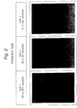
- Figure 2 is a series of photographs illustrating the discoloration of copper foil reported in the Table.
- the composite foil of the present invention is characterized by having a protective layer of porous copper and interpenetrating zinc between an aluminum carrier layer and an ultra-thin copper foil.
- the protective layer serves as a release layer and provides a bond strength between the aluminum carrier and the ultra-thin copper foil sufficient to permit handling and lamination to an insulating substrate, but weak enough to permit separation of the aluminum carrier after lamination.
- the protective layer also provides oxidation protection to the copper foil surface so that it is not discolored when exposed to high temperatures during lamination.
- the thickness of the aluminum carrier layer is not considered to be critical, and it may be a foil from about 18-70 ⁇ m thick. Since a typical carrier layer is relatively thin, it will also be referred to as a foil, but it is to be understood that the support layer could be thicker than ordinary foils. For example, heavier carrier sheets up to about 5 mm thick may be used.
- the thickness of the ultra-thin copper foil layer to be formed on the protective layer is generally not more than 12 ⁇ m thick and may be much thinner, for example, 5-7 ⁇ m or less.
- a copper foil having a thickness of more than 12 ⁇ m can be produced by conventional processes, and can be handled without a carrier layer, although the process described herein could be used to deposit copper foils thicker than 12 ⁇ m, if desired.
- the ultra-thin copper foil layer is preferably formed by electrodeposition, although vapor deposition or electroless plating may be employed, provided that the ultra-thin copper layer is suitable for making circuit patterns and has acceptable bond and peel strengths.
- the inventors have found that electrodepositing zinc (or using the zincate process) directly on an aluminum carrier, followed by electrodeposition of an ultra-thin copper foil, produces a composite which has a bond strength which is so strong that the aluminum carrier cannot be readily separated after the ultra-thin copper foil has been laminated to an insulating substrate.
- the aluminum carrier is typically removed by chemical etching, which is an undesirable method. It is more expensive and involves disposal of caustic solutions. If copper is electrodeposited directly on an aluminum carrier, however, the bond strength is too weak.
- the present invention provides a method for obtaining suitable bond strength while, at the same time, protecting the ultra-thin copper foil after it is separated from the aluminum carrier.
- the range of the bond strengths between the ultra-thin copper foil and the aluminum carrier is about 1-50 gf/cm (gm force/cm width), preferably 1-2 gf/cm, to assure that the carrier layer can be separated from the ultra-thin copper foil after laminating the composite foil on an insulating substrate.
- This bond strength is relatively low, but it is sufficient to permit handling. It is uniform, and the carrier can easily be removed after the ultra-thin copper foil has been laminated to a substrate.
- the bond strength is so weak that bulging or separating of the ultra-thin copper foil occurs during lamination with a substrate or during punching or drilling of a laminate or a circuit board.
- the bond strength is so large that it is not possible to separate the carrier or it is necessary to provide a special treatment as, for example, the use of an aqueous medium in U.S. Patent No. 3,886,022.
- a composite foil of the invention has little or no variability in the bond strength between the aluminum carrier layer and the ultra-thin copper foil.
- the bond strength is consistent both across individual composite foils and among multiple examples of the composite foil.
- the protective layer is formed on the aluminum carrier layer and, thereafter, an ultra-thin copper layer is deposited on the protective layer.
- Pretreatment of the aluminum carrier layer is desirable in order to clean it and to remove aluminum oxide, thus providing a clean surface for deposition of the protective layer. Since the bond strength should be uniform if the carrier is to be easily separated from the ultra-thin copper foil, this pretreatment helps to assure consistent results.
- a caustic bath is used for pretreatment of the aluminum carrier. In the Examples below, an aqueous bath containing sodium hydroxide, potassium sodium tartrate tetrahydrate, and sodium carbonate is used. The aluminum is dipped in the bath and then rinsed in deionized water before electrodepositing the protective layer of porous copper and interpenetrating zinc.
- a porous layer of copper is electrodeposited.
- the porous copper layer may be deposited from a copper pyrophosphate bath, as in the Examples, although it is believed that using a copper sulfate or other bath suitable for electrodepositing copper could be used.
- a copper layer which is either too thick or too thin produces undesirable properties. It is considered to be sufficiently porous so that zinc can penetrate through it.
- the resulting zinc-containing layer has the needed bond strength. It has been found that a layer of copper of about 500-4000 mg/m 2 of aluminum is suitable, preferably about 500-3000 mg/m 2 , as will be seen in the Table below. If the amount of copper deposited is less, the bond strength is too strong. If the amount of copper is greater, the bond strength is too low.
- the zinc is preferably electrodeposited, with about 15-150 mg/m 2 of aluminum found to give suitable bond strength, preferably about 50-100 mg/m 2 .
- the protective layer consists of a small amount of zinc relative to the amount of copper. Even so, the aluminum carrier surface is only partially covered by the copper deposit, as is shown in Figure 1. This should permit access of zinc to the surface of the aluminum carrier which might be expected to produce a non-uniform bond strength.
- the results shown in the Examples suggest that the zinc is not deposited directly on the aluminum, but is preferentially deposited on the copper and penetrates through it to the aluminum. Whether this is a correct conclusion or not, the effect on the bond strength between the aluminum carrier and the ultra-thin copper foil shown in the Examples is clear. It can be seen that the bond strength does not vary significantly with the amount of copper deposited. When the amount of copper is 1000 mg/m 2 , a significant portion of the aluminum surface is still exposed ( Figure 1).
- the ultra-thin copper foil preferably is electrodeposited on top of the protective layer which has been placed on the aluminum carrier.
- two methods of electrodepositing copper are used.
- a copper pyrophosphate bath gives a more uniform electrodeposition of copper. More importantly, it does not tend to dissolve the zinc, which would occur if an acidic copper sulfate bath were to be used.
- Copper pyrophosphate plating is preferred since it has advantages with respect to the environment and safety of operations, but a copper cyanide bath may also be used. Copper sulfate plating baths are advantageous if one considers productivity and cost.
- a first copper plating step providing a thickness sufficient to cover the zinc, typically at least 3000 mg/m 2 is done in a copper pyrophosphate bath, followed by a second plating step using a copper sulfate plating bath to provide the desired thickness of the ultra-thin copper foil.
- This method is used in the Examples below.
- the conditions for copper pyrophosphate plating are not believed to be critical. It is preferred, however, that the copper concentration in the copper pyrophosphate plating bath be about 10-50 g/L and the potassium pyrophosphate about 100-700 g/L.
- the pH of the electrolytic solution preferably should be about 7-12.
- the bath temperature should be about 30-60°C, and the current density about 1-10 A/dm 2 .
- the conditions for acidic copper sulfate plating are also not considered critical. It is preferred, however, that the copper concentration in the copper sulfate plating bath be about 30-100 g/L, and that the sulfuric acid be about 50-200 g/L.
- the bath temperature of electrolytic solution preferably is about 30-80°C and the current density about 10-100 A/dm 2 .
- the conditions for zinc plating are not considered to be critical. It is preferred, however, that the zinc concentration be about 1-10 g/L as zinc pyrophosphate and potassium pyrophosphate be present at about 50-500 g/L.
- the bath temperature is preferably about 20-60°C, and the current density is about 0.1-5 A/dm 2 .
- the ultra-thin copper foil layer may be subjected to a peel enhancing treatment by conventional methods, such as forming a nodular copper deposit on the surface of the foil by adjusting plating conditions.
- a nodularization process may be found in U.S. Patent No. 3, 674, 656.
- the surface of the ultra-thin copper foil may be subjected to a conventional passivation treatment, such as by depositing zinc, zinc chromate, nickel, tin, cobalt and chromium on the nodularized ultra-thin copper layer.
- a conventional passivation treatment such as by depositing zinc, zinc chromate, nickel, tin, cobalt and chromium on the nodularized ultra-thin copper layer.
- An example of such methods may be found in U.S. Patent No. 3,625,844.
- the surface of the treated ultra-thin copper foil produced by the methods just described will be laminated to an insulating substrate using heat and pressure to obtain a copper-clad laminate.
- the insulating substrate any of the resin substrates which are used to make circuit boards for electronic equipment can be used.
- Such resin substrates may include FR-4 (glass-fiber-epoxy), paper-phenolic, paper-epoxy, polyimides and the like.
- the aluminum carrier layer is then separated, leaving a copper-clad laminate consisting of the ultra-thin copper foil with its protective layer exposed and the insulating substrate.
- a printed wiring board is made by forming wiring patterns from the exposed ultra-thin copper layer.
- an aluminum foil having a thickness of 40 ⁇ m was chosen.
- the foil was pretreated, and then a porous layer of copper was electrodeposited, followed by electroplating with zinc. Then, the aluminum covered with the protective layer of copper and zinc was given a first copper plating step and a second copper plating step using the following procedures.
- the 40 ⁇ m aluminum foil was dipped into an aqueous solution containing 30 g/L of NaOH, 46 g/L of potassium sodium tartrate tetrahydrate, and 46 g/L of sodium carbonate at 40°C for 27 seconds, removed, and rinsed in deionized water for 10 seconds to prepare the aluminum surface for electrodeposition of the protective layer.
- the pretreated aluminum carrier foil was placed in an aqueous copper pyrophosphate bath having a pH of 8.5 and containing 55.89 g/L copper pyrophosphate and 290 g/L of potassium pyrophosphate at a temperature of 50°C. A current density of 2.7 A/dm 2 was used. Copper was plated on the aluminum for a time sufficient to deposit the desired amount of copper, as shown in the Table below.
- the aluminum foil containing the desired amount of copper was placed in a zinc pyrophosphate bath at 40°C and a pH of 10.5 to deposit the desired amount of zinc.
- the bath contained 14 g/L of zinc pyrophosphate and 100 g/L of potassium pyrophosphate.
- a cathodic electroplating treatment was carried out with a current density of 2.7 A/dm 2 by using a copper pyrophosphate plating bath, with a bath temperature of 50°C and a pH of 8.5.
- the bath contained 55.89 g/L of copper pyrophosphate and 290 g/L of potassium pyrophosphate.
- a copper deposit of about 3000 mg/m 2 having a thickness of 0.3 ⁇ m was deposited on the protective release layer.
- the surface of the initial copper deposit was rinsed in deionized water and then electroplated at a current density of 10 A/dm 2 using a copper sulfate plating bath at a temperature of 40°C, and containing 216 g/L of copper sulfate pentahydrate and 150 g/L sulfuric acid, to deposit about 5 ⁇ m thickness of copper.
- the composite foil was laminated on four sheets of FR-4, and then hot pressed under a pressure of 25 kg/cm 2 at 175°C for 60 minutes to obtain a copper-clad laminate.
- the strength of the bond between the ultra-thin copper foil and the 45 ⁇ m aluminum carrier layer was measured in accordance with JIS-C-6481 before and after lamination.
- the discoloration of the exposed copper surface after separation was also determined and given a rating shown in the Table below. The ratings are illustrated by the photographs of Figure 2.
- Example 1 The following general conclusions may be drawn from the results of Example 1.
- the relative size of the porous copper and zinc deposits was the principal reason for the bond strength and surface discoloration which was measured. It appears that increasing the amount of zinc present produces the least discoloration. This indicates that zinc is penetrating the copper deposit to reach the aluminum-copper interface. It is preferred that at least 50 mg of zinc for each m 2 of aluminum is used.
- the ratio of copper to zinc does not appear to have a significant effect on the bond strength after lamination, which is an unexpected observation. It appears, however, that there is a maximum amount of zinc which can be deposited, even when the copper deposit is relatively heavy.
- a composite foil was made in the same manner as in Example 1, except that only the porous copper was deposited and deposition of zinc and the first thin copper layer was omitted. The results are shown in the Table below. The bond strength was too low before lamination and negligible after lamination. The surface discoloration rating was poor.
- a composite foil was made in the same manner as in Example 1, except that the porous copper layer was omitted and the zinc was deposited by the zincate replacement reaction. The results are shown in the Table below.
- the aluminum foil carrier could not be separated, either before or after lamination.
- a composite foil was made as in Example 1, except that the porous copper deposit was too high. As shown in the Table below, the bond strength was too low, both before and after lamination.
- a composite foil was prepared according to Example 1, except that the zinc was supplied by the zincate treatment. In the case, the aluminum foil could not be separated from the ultra-thin copper foil after lamination.
Landscapes
- Chemical & Material Sciences (AREA)
- Engineering & Computer Science (AREA)
- Chemical Kinetics & Catalysis (AREA)
- Electrochemistry (AREA)
- Materials Engineering (AREA)
- Metallurgy (AREA)
- Organic Chemistry (AREA)
- Manufacturing & Machinery (AREA)
- Microelectronics & Electronic Packaging (AREA)
- Laminated Bodies (AREA)
- Parts Printed On Printed Circuit Boards (AREA)
- Electroplating Methods And Accessories (AREA)
- Production Of Multi-Layered Print Wiring Board (AREA)
- Manufacturing Of Printed Wiring (AREA)
Applications Claiming Priority (2)
| Application Number | Priority Date | Filing Date | Title |
|---|---|---|---|
| US131160 | 1987-12-10 | ||
| US09/131,160 US6183880B1 (en) | 1998-08-07 | 1998-08-07 | Composite foil of aluminum and copper |
Publications (2)
| Publication Number | Publication Date |
|---|---|
| EP0987931A2 true EP0987931A2 (de) | 2000-03-22 |
| EP0987931A3 EP0987931A3 (de) | 2002-04-24 |
Family
ID=22448170
Family Applications (1)
| Application Number | Title | Priority Date | Filing Date |
|---|---|---|---|
| EP99306233A Withdrawn EP0987931A3 (de) | 1998-08-07 | 1999-08-05 | Verbundfolie aus Aluminium und Kupfer |
Country Status (7)
| Country | Link |
|---|---|
| US (1) | US6183880B1 (de) |
| EP (1) | EP0987931A3 (de) |
| JP (1) | JP3180101B2 (de) |
| KR (1) | KR100614859B1 (de) |
| CN (1) | CN1179611C (de) |
| MY (1) | MY115624A (de) |
| SG (1) | SG77265A1 (de) |
Cited By (2)
| Publication number | Priority date | Publication date | Assignee | Title |
|---|---|---|---|---|
| EP1401659A4 (de) * | 2001-02-23 | 2005-05-04 | Nikko Materials Usa Inc | Korrosionsschutz für cac-komponente |
| EP1564311A4 (de) * | 2002-10-25 | 2007-08-15 | Fcm Co Ltd | Stabilisiertes aluminiumlaminat aus aluminium mit stabilisierungsschicht |
Families Citing this family (34)
| Publication number | Priority date | Publication date | Assignee | Title |
|---|---|---|---|---|
| US6346335B1 (en) * | 2000-03-10 | 2002-02-12 | Olin Corporation | Copper foil composite including a release layer |
| US6569543B2 (en) | 2001-02-15 | 2003-05-27 | Olin Corporation | Copper foil with low profile bond enahncement |
| JP3743702B2 (ja) * | 2000-04-28 | 2006-02-08 | 三井金属鉱業株式会社 | プリント配線板のセミアディティブ製造法 |
| US6447929B1 (en) * | 2000-08-29 | 2002-09-10 | Gould Electronics Inc. | Thin copper on usable carrier and method of forming same |
| US6893742B2 (en) * | 2001-02-15 | 2005-05-17 | Olin Corporation | Copper foil with low profile bond enhancement |
| JP2002294484A (ja) * | 2001-04-03 | 2002-10-09 | Mitsui Mining & Smelting Co Ltd | ピロりん酸銅めっき浴及びピロりん酸亜鉛メッキ浴並びにこれらのメッキ浴を用いたメッキ方法 |
| JP4582436B2 (ja) * | 2001-08-27 | 2010-11-17 | Jx日鉱日石金属株式会社 | 水溶性樹脂キャリア付銅箔及び該銅箔を使用したプリント基板 |
| US20030102073A1 (en) * | 2001-12-03 | 2003-06-05 | Pioneer Technology Engineering Co., Ltd. | Method for manufacturing a copper-clad laminate |
| JP3977790B2 (ja) * | 2003-09-01 | 2007-09-19 | 古河サーキットフォイル株式会社 | キャリア付き極薄銅箔の製造方法、及び該製造方法で製造された極薄銅箔、該極薄銅箔を使用したプリント配線板、多層プリント配線板、チップオンフィルム用配線基板 |
| US6872468B1 (en) * | 2003-10-09 | 2005-03-29 | Motorola, Inc. | Peelable circuit board foil |
| US7132158B2 (en) * | 2003-10-22 | 2006-11-07 | Olin Corporation | Support layer for thin copper foil |
| JP3972895B2 (ja) * | 2003-12-10 | 2007-09-05 | 松下電器産業株式会社 | 回路基板の製造方法 |
| US7138068B2 (en) * | 2005-03-21 | 2006-11-21 | Motorola, Inc. | Printed circuit patterned embedded capacitance layer |
| US7241510B2 (en) * | 2005-05-27 | 2007-07-10 | Motorola, Inc. | Peelable circuit board foil |
| JP4934409B2 (ja) * | 2005-12-15 | 2012-05-16 | 古河電気工業株式会社 | キャリア付き極薄銅箔及びプリント配線基板 |
| JP4927503B2 (ja) * | 2005-12-15 | 2012-05-09 | 古河電気工業株式会社 | キャリア付き極薄銅箔及びプリント配線基板 |
| WO2007106502A2 (en) * | 2006-03-13 | 2007-09-20 | Nanogram Corporation | Thin silicon or germanium sheets and photovoltaics formed from thin sheets |
| JP5196102B2 (ja) * | 2007-01-12 | 2013-05-15 | 上村工業株式会社 | アルミニウム酸化皮膜用除去液及びアルミニウム又はアルミニウム合金の表面処理方法 |
| EP2312022A4 (de) * | 2008-07-22 | 2012-11-14 | Furukawa Electric Co Ltd | Oberflächenbehandelte kupferfolie und kupferkaschiertes laminat |
| KR101045002B1 (ko) | 2008-08-13 | 2011-06-29 | 한국과학기술원 | 전해도금법에 의한 다공성 구리의 제조방법 |
| CN101768768B (zh) * | 2008-12-26 | 2012-01-25 | 比亚迪股份有限公司 | 一种铝合金无氰无镍电镀方法及其电镀产品 |
| US8835319B2 (en) | 2012-03-02 | 2014-09-16 | Infineon Technologies Ag | Protection layers for conductive pads and methods of formation thereof |
| JP6599853B2 (ja) | 2013-06-21 | 2019-10-30 | サンミナ コーポレーション | 除去可能なカバー層を用いてめっき貫通孔を有する積層構造を形成する方法 |
| TW201522071A (zh) * | 2013-09-10 | 2015-06-16 | Dainippon Ink & Chemicals | 積層體、導電性圖案、電路及積層體之製造方法 |
| US9758889B2 (en) * | 2014-05-08 | 2017-09-12 | Ymt Co., Ltd. | Method for producing substrate formed with copper thin layer, method for manufacturing printed circuit board and printed circuit board manufactured thereby |
| KR101944784B1 (ko) * | 2017-01-16 | 2019-02-08 | 일진머티리얼즈 주식회사 | 캐리어박 부착 극박동박 |
| KR101944783B1 (ko) * | 2017-01-16 | 2019-04-18 | 일진머티리얼즈 주식회사 | 캐리어박 부착 극박동박 |
| KR102044155B1 (ko) | 2018-09-20 | 2019-12-02 | 영원산업개발 주식회사 | 회전식 빛 반사 조명구 |
| CN110785015A (zh) * | 2018-12-10 | 2020-02-11 | 广州方邦电子股份有限公司 | 一种复合金属箔 |
| KR20210078158A (ko) | 2019-12-18 | 2021-06-28 | 박문화 | 회전식 조명등 |
| CN112002752B (zh) | 2020-07-27 | 2023-04-21 | 北海惠科光电技术有限公司 | 源漏电极的制备方法、阵列基板的制备方法和显示机构 |
| CN112930024B (zh) * | 2021-01-25 | 2022-05-03 | 景旺电子科技(龙川)有限公司 | 金属基线路板及其制作方法 |
| CN113416986B (zh) * | 2021-07-08 | 2022-10-11 | 江西柔顺科技有限公司 | 电解铜箔的制造方法 |
| CN120290922B (zh) * | 2025-06-12 | 2025-08-22 | 浙江省冶金研究院有限公司 | 一种铜银合金及其制备方法 |
Family Cites Families (11)
| Publication number | Priority date | Publication date | Assignee | Title |
|---|---|---|---|---|
| BE788117A (fr) | 1971-08-30 | 1973-02-28 | Perstorp Ab | Procede de production d'elements pour circuits imprimes |
| US3936548A (en) | 1973-02-28 | 1976-02-03 | Perstorp Ab | Method for the production of material for printed circuits and material for printed circuits |
| DE2413932C2 (de) | 1973-04-25 | 1984-08-30 | Yates Industries, Inc., Bordentown, N.J. | Verfahren zum Herstellen einer Verbundfolie für die Ausbildung gedruckter Schaltkreise |
| SE7308653L (de) * | 1973-06-20 | 1974-12-23 | Perstorp Ab | |
| US3998601A (en) | 1973-12-03 | 1976-12-21 | Yates Industries, Inc. | Thin foil |
| US4088544A (en) | 1976-04-19 | 1978-05-09 | Hutkin Irving J | Composite and method for making thin copper foil |
| US4293617A (en) | 1979-12-26 | 1981-10-06 | Gould Inc. | Process for producing strippable copper on an aluminum carrier and the article so obtained |
| US4357395A (en) | 1980-08-22 | 1982-11-02 | General Electric Company | Transfer lamination of vapor deposited foils, method and product |
| EP0208177A3 (de) | 1985-07-05 | 1988-09-14 | Yates Industries, Inc. | Äusserst dünne Kupferfolie und Verfahren zur Herstellung einer solchen Folie |
| US5057372A (en) * | 1989-03-22 | 1991-10-15 | The Dow Chemical Company | Multilayer film and laminate for use in producing printed circuit boards |
| SE9203327L (sv) | 1992-11-06 | 1993-12-20 | Metfoils Ab | Förfarande vid mönsterkortstillverkning samt användning därvid |
-
1998
- 1998-08-07 US US09/131,160 patent/US6183880B1/en not_active Expired - Fee Related
-
1999
- 1999-08-02 JP JP21855599A patent/JP3180101B2/ja not_active Expired - Fee Related
- 1999-08-05 EP EP99306233A patent/EP0987931A3/de not_active Withdrawn
- 1999-08-06 SG SG1999003848A patent/SG77265A1/en unknown
- 1999-08-06 KR KR1019990032251A patent/KR100614859B1/ko not_active Expired - Fee Related
- 1999-08-06 CN CNB99117545XA patent/CN1179611C/zh not_active Expired - Fee Related
- 1999-08-06 MY MYPI99003357A patent/MY115624A/en unknown
Cited By (2)
| Publication number | Priority date | Publication date | Assignee | Title |
|---|---|---|---|---|
| EP1401659A4 (de) * | 2001-02-23 | 2005-05-04 | Nikko Materials Usa Inc | Korrosionsschutz für cac-komponente |
| EP1564311A4 (de) * | 2002-10-25 | 2007-08-15 | Fcm Co Ltd | Stabilisiertes aluminiumlaminat aus aluminium mit stabilisierungsschicht |
Also Published As
| Publication number | Publication date |
|---|---|
| MY115624A (en) | 2003-07-31 |
| US6183880B1 (en) | 2001-02-06 |
| JP2000059035A (ja) | 2000-02-25 |
| EP0987931A3 (de) | 2002-04-24 |
| JP3180101B2 (ja) | 2001-06-25 |
| CN1244460A (zh) | 2000-02-16 |
| KR20000017134A (ko) | 2000-03-25 |
| CN1179611C (zh) | 2004-12-08 |
| SG77265A1 (en) | 2000-12-19 |
| KR100614859B1 (ko) | 2006-08-22 |
Similar Documents
| Publication | Publication Date | Title |
|---|---|---|
| US6183880B1 (en) | Composite foil of aluminum and copper | |
| EP0930811B1 (de) | Kupfer-Verbundfolie, Verfahren zu deren Herstellung, und kupferkaschiertes Laminat und Leiterplatte unter Verwendung derselben | |
| JP4728723B2 (ja) | キャリア付き極薄銅箔 | |
| EP1420621B1 (de) | Ultradünne Kupferfolie mit Träger, Herstellungsverfahren dieses Systems und Leiterplatte mit dessen Verwendung | |
| US5389446A (en) | Copper foil for printed circuits | |
| EP1407062B1 (de) | Verbundfolie und herstellungsverfahren dafür | |
| US6548153B2 (en) | Composite material used in making printed wiring boards | |
| KR102694343B1 (ko) | 프린트 배선판 제조용 구리박, 캐리어를 구비한 구리박 및 동장 적층판 그리고 그것들을 사용한 프린트 배선판의 제조 방법 | |
| US6319620B1 (en) | Making and using an ultra-thin copper foil | |
| JP2004169181A (ja) | キャリア付き極薄銅箔、及びその製造方法、キャリア付き極薄銅箔を用いたプリント配線基板 | |
| KR102915622B1 (ko) | 프린트 배선판 제조용 금속박, 캐리어를 구비하는 금속박, 금속 클래드 적층판, 및 프린트 배선판의 제조 방법 | |
| JP3392066B2 (ja) | 複合銅箔およびその製造方法並びに該複合銅箔を用いた銅張り積層板およびプリント配線板 | |
| EP0996318B1 (de) | Neue Verbundfolie, Verfahren zu deren Herstellung und Kupferkaschiertes Laminat | |
| EP1089603A2 (de) | Behandlung von Kupferfolie mit verbesserter Bindungsfestigkeit und Unterätzung | |
| CA2070046A1 (en) | Metal foil with improved bonding to substrates and method for making said foil | |
| JP3615973B2 (ja) | 新規な複合箔およびその製造方法、銅張り積層板 | |
| JP4748519B2 (ja) | キャリア付き極薄銅箔、及びその製造方法、キャリア付き極薄銅箔を用いたプリント配線基板 | |
| JPH0654829B2 (ja) | 印刷回路用銅箔の処理方法 | |
| JPH08335775A (ja) | 印刷回路用銅箔の処理方法 | |
| HK1023092A (en) | Composite foil of aluminum and copper | |
| GB2185757A (en) | Dendritic surface treatment of metal layers | |
| JP2000196226A (ja) | 電気回路形成用複合材料およびその用途 | |
| JP2000315848A (ja) | 銅張り積層板の製造方法およびプリント配線板 |
Legal Events
| Date | Code | Title | Description |
|---|---|---|---|
| PUAI | Public reference made under article 153(3) epc to a published international application that has entered the european phase |
Free format text: ORIGINAL CODE: 0009012 |
|
| AK | Designated contracting states |
Kind code of ref document: A2 Designated state(s): AT BE CH CY DE DK ES FI FR GB GR IE IT LI LU MC NL PT SE Kind code of ref document: A2 Designated state(s): DE FR GB LU |
|
| AX | Request for extension of the european patent |
Free format text: AL;LT;LV;MK;RO;SI |
|
| PUAL | Search report despatched |
Free format text: ORIGINAL CODE: 0009013 |
|
| AK | Designated contracting states |
Kind code of ref document: A3 Designated state(s): AT BE CH CY DE DK ES FI FR GB GR IE IT LI LU MC NL PT SE |
|
| AX | Request for extension of the european patent |
Free format text: AL;LT;LV;MK;RO;SI |
|
| RIC1 | Information provided on ipc code assigned before grant |
Free format text: 7H 05K 3/38 A, 7C 25D 5/10 B, 7C 25D 1/04 B, 7H 05K 3/02 B, 7C 25D 1/20 B |
|
| 17P | Request for examination filed |
Effective date: 20020726 |
|
| AKX | Designation fees paid |
Free format text: DE FR GB LU |
|
| STAA | Information on the status of an ep patent application or granted ep patent |
Free format text: STATUS: THE APPLICATION HAS BEEN WITHDRAWN |
|
| 18W | Application withdrawn |
Effective date: 20030718 |