EP0991089A2 - Elément inducteur composite - Google Patents
Elément inducteur composite Download PDFInfo
- Publication number
- EP0991089A2 EP0991089A2 EP99118959A EP99118959A EP0991089A2 EP 0991089 A2 EP0991089 A2 EP 0991089A2 EP 99118959 A EP99118959 A EP 99118959A EP 99118959 A EP99118959 A EP 99118959A EP 0991089 A2 EP0991089 A2 EP 0991089A2
- Authority
- EP
- European Patent Office
- Prior art keywords
- coils
- inductor element
- composite inductor
- block
- element according
- Prior art date
- Legal status (The legal status is an assumption and is not a legal conclusion. Google has not performed a legal analysis and makes no representation as to the accuracy of the status listed.)
- Withdrawn
Links
- 239000002131 composite material Substances 0.000 title claims abstract description 64
- 239000011347 resin Substances 0.000 claims abstract description 23
- 229920005989 resin Polymers 0.000 claims abstract description 23
- 239000000696 magnetic material Substances 0.000 claims abstract description 11
- 239000004020 conductor Substances 0.000 claims description 15
- 238000004804 winding Methods 0.000 claims description 6
- 229910052709 silver Inorganic materials 0.000 claims description 4
- 238000009413 insulation Methods 0.000 claims description 3
- 229910052759 nickel Inorganic materials 0.000 claims description 2
- 239000004332 silver Substances 0.000 claims description 2
- 229910052763 palladium Inorganic materials 0.000 claims 1
- 239000011248 coating agent Substances 0.000 description 9
- 238000000576 coating method Methods 0.000 description 9
- 238000001746 injection moulding Methods 0.000 description 8
- 229910000859 α-Fe Inorganic materials 0.000 description 8
- 239000004734 Polyphenylene sulfide Substances 0.000 description 7
- 238000004519 manufacturing process Methods 0.000 description 7
- 229920000069 polyphenylene sulfide Polymers 0.000 description 7
- 230000015556 catabolic process Effects 0.000 description 6
- 239000008188 pellet Substances 0.000 description 6
- 230000008878 coupling Effects 0.000 description 5
- 238000010168 coupling process Methods 0.000 description 5
- 238000005859 coupling reaction Methods 0.000 description 5
- 230000000052 comparative effect Effects 0.000 description 4
- 238000010276 construction Methods 0.000 description 4
- 239000000463 material Substances 0.000 description 3
- 238000000034 method Methods 0.000 description 3
- 230000004048 modification Effects 0.000 description 3
- 238000012986 modification Methods 0.000 description 3
- 238000000465 moulding Methods 0.000 description 3
- 230000035699 permeability Effects 0.000 description 3
- 230000008569 process Effects 0.000 description 3
- 238000005520 cutting process Methods 0.000 description 2
- 239000002184 metal Substances 0.000 description 2
- 229910052751 metal Inorganic materials 0.000 description 2
- 239000000843 powder Substances 0.000 description 2
- RYGMFSIKBFXOCR-UHFFFAOYSA-N Copper Chemical compound [Cu] RYGMFSIKBFXOCR-UHFFFAOYSA-N 0.000 description 1
- 239000010953 base metal Substances 0.000 description 1
- 229910052802 copper Inorganic materials 0.000 description 1
- 239000010949 copper Substances 0.000 description 1
- 239000012772 electrical insulation material Substances 0.000 description 1
- 230000008030 elimination Effects 0.000 description 1
- 238000003379 elimination reaction Methods 0.000 description 1
- 230000004907 flux Effects 0.000 description 1
- 238000010438 heat treatment Methods 0.000 description 1
- 238000010030 laminating Methods 0.000 description 1
- 238000003754 machining Methods 0.000 description 1
- 238000005259 measurement Methods 0.000 description 1
- 238000007639 printing Methods 0.000 description 1
- 238000005476 soldering Methods 0.000 description 1
- 238000003466 welding Methods 0.000 description 1
Images


Classifications
-
- H—ELECTRICITY
- H01—ELECTRIC ELEMENTS
- H01F—MAGNETS; INDUCTANCES; TRANSFORMERS; SELECTION OF MATERIALS FOR THEIR MAGNETIC PROPERTIES
- H01F27/00—Details of transformers or inductances, in general
- H01F27/02—Casings
- H01F27/022—Encapsulation
-
- H—ELECTRICITY
- H01—ELECTRIC ELEMENTS
- H01F—MAGNETS; INDUCTANCES; TRANSFORMERS; SELECTION OF MATERIALS FOR THEIR MAGNETIC PROPERTIES
- H01F17/00—Fixed inductances of the signal type
- H01F17/04—Fixed inductances of the signal type with magnetic core
- H01F17/06—Fixed inductances of the signal type with magnetic core with core substantially closed in itself, e.g. toroid
Definitions
- the present invention relates to a composite inductor element. More particularly, the present invention relates to a composite inductor element constructed to function as an anti-noise component in personal computers and other electronic apparatuses.
- Personal computers have a plurality of types of power supply circuits such as power circuits to drive CPUs, power circuits to drive circuits other than the CPUs, power circuits to drive hard disks, floppy disks and the like, and so on.
- power circuits Although there are supplying currents as large as tens of amperes, as in the power circuits for driving CPUs having high clock frequencies, there are also other supplying currents as small as hundreds of milliamperes.
- an anti-noise component having a current capacity corresponding to each supply current is separately required.
- a single element having a current capacity corresponding to the current capacity of each of the power circuits has been used as an anti-noise component.
- preferred embodiments of the present invention provide a composite inductor element which has a significantly reduced cost and greatly reduced space requirement as compared to conventional anti-noise components.
- a composite inductor element includes a plurality of coils buried in a block made up of at least either resin or rubber having magnetic material dispersed therein and the end portions of each of the coils are electrically connected to external electrodes provided on the block.
- the coils have different electrical characteristics such as current capacity, inductance, and other characteristics.
- a plurality of electromagnetically close-coupled coils defined by spirally wound parallel lines are provided and a plurality of conductors integrally coated with insulating coating resin are arranged in parallel.
- the plurality of coils are buried in a block made up of at least either resin or rubber having a magnetic material dispersed therein.
- a composite inductor element acts as a common-mode choke coil, and when common mode noise is applied to each of a plurality of electromagnetically close-coupled coils, the noise is prevented from being transmitted.
- an array type composite inductor element having a plurality of common-mode choke coils embedded in a block includes a plurality of spirally wound parallel-wire lines constituting a plurality of electromagnetically close-coupled coils buried in a block while being separated from each other.
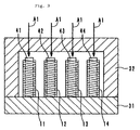
- the composite inductor element 1 includes a plurality of spirally wound coils 11, 12, 13, 14 (preferably, four coils in the first preferred embodiment) buried in a block 2.
- the block 2 preferably has a substantially rectangular parallelepiped shape and the coils 11-14 are preferably arranged such that the axes of the coils extend in the same direction.
- the block 2 is preferably made of either resin or rubber having magnetic material of ferrite or other magnetic material, dispersed therein.
- External electrodes 21a through 24a and 21b through 24b are provided, respectively, on two opposite side portions 2a and 2b of the block 2.
- the end portions 11t and 11t of the coil 11 are electrically connected to the external electrodes 21a and 21b, respectively, the end portions 12t and 12t of the coil 12 are electrically connected to the external electrodes 22a and 22b, respectively, the end portions 13t and 13t of the coil 13 are electrically connected to the external electrodes 23a and 23b, respectively, and the end portions 14t and 14t of the coil 14 are electrically connected to the external electrodes 24a and 24b, respectively.
- the external electrodes 21a through 24a and 21b through 24b can be formed, for example, by applying and hardening conductive paste of Ag, Ag-Pd, Ni, and other suitable material, on the side portions 2a and 2b of the block 2. Further, the external electrodes 21a through 24b may be constructed using metal caps preferably having a substantially U-shape which is made up of silver or other suitable material. After the metal caps have been attached to the side portions 2a and 2b of the block 2, the caps are electrically connected to the end portions 11t through 14t of the coils 11 through 14 preferably via soldering or spot welding.
- a composite inductor element 1 having such a construction is mounted, for example, as an anti-noise element for power circuits in personal computers.
- the coils constructed in accordance with the noise and current capacity specifications of the power circuits in the personal computers where the element 1 is to be mounted are buried inside of the block 2.
- a plurality of conventional anti-noise elements are realized in a single unit. Accordingly, the cost of providing anti-noise measures is greatly reduced and the space occupied by anti-noise elements is greatly reduced.
- pellets of PPS resin polyphenylene sulfide resin
- sets of spirally wound coils 11 through 14, which are needed for one molding shot, are prepared.
- the molded part 34 is cut at locations shown by one-dot chain lines L1 using a slicing machine, a dicing cutter, or other suitable device, to produce blocks 2.
- the blocks 2 are further cut at the locations shown by one-dot chain lines L2 in Fig. 5 and the end portions 11t through 14t of the coils 11 through 14, respectively, buried inside of the blocks 2 become exposed on the surface of the blocks 2.
- conductive paste is applied and hardened on the side portions 2a and 2b where the end portions 11t through 14t of the coils 11 through 14, respectively, are exposed.
- the external electrodes 21a through 24a and 21b through 24b electrically connected to the end portions 11t through 14t of the coils 11 through 14, respectively, are formed. In this way, via a molding process and a cutting process using resin material suitable for mass production, a composite inductor element 1 can be efficiently manufactured.
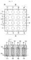
- a composite inductor element 51 the plan view of which is shown in Fig. 6, four coils 61 through 64 having different numbers of windings (that is, different inductances), which are different from those of the composite inductor element 1 of the first preferred embodiment, are buried in a block 2.
- the number of windings of the coils 61 through 64 is determined individually based on the noise and current capacity specifications of the power circuits of the personal computers or other electronic apparatuses, to which the composite inductor element 51 is connected.
- external electrodes 21a through 24a and 21b through 24b are provided, respectively.
- End portions 61t and 61t of the coil 61 are electrically connected to the external electrodes 21a and 21b, respectively, end portions 62t and 62t of the coil 62 are electrically connected to the external electrodes 22a and 22b, respectively, end portions 63t and 63t of the coil 63 are electrically connected to the external electrodes 23a and 23b, respectively, and end portions 64t and 64t of the coil 64 are electrically connected to the external electrodes 24a and 24b, respectively.
- a composite inductor element 71 the plan view of which is shown in Fig. 7, four coils 61a through 64a having different numbers of windings and different coil wire thicknesses and different coil diameters, which are different from the case of the composite inductor element 1 of the first preferred embodiment, are buried in a block 2.
- the wire thicknesses, numbers of windings, and coil diameters of the coils 61a through 64a are determined individually based on the noise and current capacity specifications of the power circuits of the personal computers or other electronic apparatuses to which the composite inductor element 71 is connected.
- external electrodes 21a through 24a and 21b through 24b are provided, respectively.
- End portions 61t and 61t of the coil 61a are electrically connected to the external electrodes 21a and 21b, respectively, end portions 62t and 62t of the coil 62a are electrically connected to the external electrodes 22a and 22b, respectively, end portions 63t and 63t of the coil 63a are electrically connected to the external electrodes 23a and 23b, respectively, and end portions 64t and 64t of the coil 64a are electrically connected to the external electrodes 24a and 24b, respectively.
- a combination of coils 61 through 64 and 61a through 64a can be changed, for example, in accordance with the current capacity and noise elimination characteristics corresponding to a plurality of power circuits of personal computers or other electronic apparatuses.
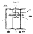
- the composite inductor element 81 preferably includes two electromagnetically close-coupled coils 91 and 92.
- the two coils 91 and 92 are preferably made of a parallel-wire line 94 in which two conductors 91a and 92a integrally coated with insulating coating resin 93 are arranged in parallel.
- the parallel-wire line 94 is spirally wound around one coil axis and buried in a block 2 having a substantially rectangular parallelepiped shape.
- the block 2 is preferably made of either resin or rubber having magnetic material of ferrite or other magnetic material dispersed therein.
- external electrodes 21a and 21b, and 22a and 22b are provided on two opposite side portions 2a and 2b of the block 2.
- the end portions 91t and 91t of the coil 91 are electrically connected to the external electrodes 21a and 21b, respectively, and the end portions 92t and 92t (not illustrated) of the coil 92 are electrically connected to the external electrodes 22a and 22b, respectively.
- the two coils 91 and 92 are arranged to be parallel in the insulating coating resin 93 and are electromagnetically close-coupled. Accordingly, the composite inductor array element 81 is a common-mode choke coil of a bifilar type. When common mode noise is applied to each of the coils 91 and 92, the noise is prevented from being transmitted therethrough. Further, because the coils 91 and 92 are made up of conductors 91a and 91b, the cross section of which can be made relatively large, the current capacity is greatly increased in comparison with a composite inductor element of a conventional laminated type where the conductors constituting coils are formed by printing conductive paste. Further, because the two conductors 91a and 92a constituting the two coils 91 and 92 are covered by insulating coating resin 93, the reliability of the insulation between the two coils 91 and 92 is also increased.
- pellets of PPS resin mixed with ferrite powder are prepared. Further, the coils 91 and 92 made up of the parallel-wire line 94 of the two conductors 91a and 92a contained within the insulating resin 93, which is spirally wound around one coil axis, are prepared.
- both of the end portions of the molded part are cut off using a slicing machine, a dicing cutter, or other suitable cutting apparatus, to produce the block 2.
- the end portions 91t and 92t of the coils 91 and 92 are exposed.
- a guide groove 95 is formed on the side portions 2a and 2b of the block 2. In accordance with this guide groove 95, the end portions 91t and 92t of the coils 91 and 92 are guided respectively, and the end portions 91t and 92t are set within the guide groove 95.
- Example 1 Information on the breakdown voltage, the coupling coefficient, and the direct-current resistance of the composite inductor element 81 manufactured in this way are shown in Table 1.
- Table 1 for comparison, the measurements of laminated-type composite inductor elements, in which a plurality of magnetic layers and two sets of conductors defining coils are alternately laminated, are also shown (see Comparative Example 1 and Comparative Example 2).
- Example 1 was constructed by simply laminating each layer of conductors for defining the coils.
- Example 2 was constructed by arranging electrical insulation material having lower permeability than that of the magnetic layer between the conductor layers defining the coils.
- Breakdown voltage Coupling coefficient DC resistance Preferred Embodiment 100 V 99 % 10 m Comparative Example 1 50 V 80 % 1 Comparative Example 2 16 V 95 % 1
- the composite inductor element 81 of this preferred embodiment has superior reliability of insulation and a high coupling coefficient. Because the insulating coating resin 93 of the parallel-wire line 94 has a high breakdown voltage, the high breakdown voltage of the preferred embodiment was achieved, and thus, selection of the resin to be used the breakdown voltage can be further improved. Further, in the composite inductor element 81, the permeability of the block 2 is about 13, but on the other hand, the permeability of the insulating coating resin 93 is about 1 and the magnetic reluctance is relatively high.
- the ratio of the magnetic flux leaking from the coils 91 and 92 is relatively smaller than that of the laminated-type composite inductor elements, and the coupling coefficient is greatly improved. Furthermore, in the composite inductor element 81, because the conductors of relatively large thickness and made of base metal such as copper and so on can be used as the conductors 91a and 92a, the problem of wire breakage caused by heating due to a large current is solved.
- three electromagnetically close-coupled coils 96, 97, and 98 spirally wound around one coil axis may be formed using a parallel-wire line 99 in which three (or more than three) conductors 96a, 97a, and 98a are arranged in parallel in an insulating coating resin 93, and buried in a block 2 with magnetic material dispersed therein.
- the end portions 96t through 98t of the coils 96 through 98 are electrically connected to external electrodes 21a through 23a and 21b through 23b.
- the number of parallel-wire lines is not limited to one, and a plurality of spirally wound parallel-wire lines may be buried in a block such that the lines are separated from each other.
- a plurality of common-mode choke coils are contained in the block 2, the occupied space can also be further reduced.
- the present invention is not limited to the above preferred embodiments, but various modifications are possible within the spirit and scope of the invention.
- the number of coils are not limited to four, and may be changed to any arbitrary number in accordance with the specification of equipment or product in which an anti-noise component is mounted. Further, apart from a spirally wound form, the coils may be of a linear form or other suitable form.
- a plurality of anti-noise components are able to be realized as single-type units.
- the cost of anti-noise measures can be greatly reduced.
- a plurality of electromagnetically close-coupled coils are constructed by spirally winding a parallel-wire line in which a plurality of conductors are integrally coated with insulating coating resin and arranged in parallel and buried in a block, a composite inductor element functioning as a common-mode choke coil having a high breakdown voltage, a large coupling coefficient, and a large current capacity can be obtained.
Landscapes
- Engineering & Computer Science (AREA)
- Power Engineering (AREA)
- Microelectronics & Electronic Packaging (AREA)
- Coils Or Transformers For Communication (AREA)
Applications Claiming Priority (2)
| Application Number | Priority Date | Filing Date | Title |
|---|---|---|---|
| JP27486198 | 1998-09-29 | ||
| JP10274861A JP2000106312A (ja) | 1998-09-29 | 1998-09-29 | 複合インダクタ素子 |
Publications (2)
| Publication Number | Publication Date |
|---|---|
| EP0991089A2 true EP0991089A2 (fr) | 2000-04-05 |
| EP0991089A3 EP0991089A3 (fr) | 2000-09-13 |
Family
ID=17547605
Family Applications (1)
| Application Number | Title | Priority Date | Filing Date |
|---|---|---|---|
| EP99118959A Withdrawn EP0991089A3 (fr) | 1998-09-29 | 1999-09-27 | Elément inducteur composite |
Country Status (4)
| Country | Link |
|---|---|
| US (1) | US6950006B1 (fr) |
| EP (1) | EP0991089A3 (fr) |
| JP (1) | JP2000106312A (fr) |
| SG (1) | SG81314A1 (fr) |
Cited By (1)
| Publication number | Priority date | Publication date | Assignee | Title |
|---|---|---|---|---|
| EP2551864A4 (fr) * | 2010-03-20 | 2014-11-05 | Daido Steel Co Ltd | Procédé de fabrication de corps de bobine encaissé et corps de bobine encaissé |
Families Citing this family (13)
| Publication number | Priority date | Publication date | Assignee | Title |
|---|---|---|---|---|
| WO2004019352A1 (fr) * | 2002-08-26 | 2004-03-04 | Matsushita Electric Industrial Co., Ltd. | Element magnetique a utilisation multiphase et procede de production correspondant |
| JP4140632B2 (ja) * | 2002-12-13 | 2008-08-27 | 松下電器産業株式会社 | 多連チョークコイルおよびそれを用いた電子機器 |
| TW200941515A (en) * | 2008-03-17 | 2009-10-01 | Cyntec Co Ltd | Inductor and method for making thereof |
| US8692639B2 (en) * | 2009-08-25 | 2014-04-08 | Access Business Group International Llc | Flux concentrator and method of making a magnetic flux concentrator |
| JP5556284B2 (ja) * | 2010-03-20 | 2014-07-23 | 大同特殊鋼株式会社 | コイル複合成形体の製造方法及びコイル複合成形体 |
| US8698579B2 (en) * | 2010-03-31 | 2014-04-15 | Virginia Tech Intellectual Properties, Inc. | Multi-phase EMI noise separator |
| JP5689091B2 (ja) * | 2012-03-30 | 2015-03-25 | 東光株式会社 | 面実装マルチフェーズインダクタの製造方法 |
| US20130300529A1 (en) * | 2012-04-24 | 2013-11-14 | Cyntec Co., Ltd. | Coil structure and electromagnetic component using the same |
| EP4016741A1 (fr) | 2014-11-18 | 2022-06-22 | CommScope Technologies LLC | Éléments de bande basse masqués pour réseaux rayonnants multibande |
| KR102463331B1 (ko) * | 2017-10-16 | 2022-11-04 | 삼성전기주식회사 | 인덕터 어레이 |
| JP6954478B2 (ja) * | 2018-08-17 | 2021-10-27 | 株式会社村田製作所 | 平面アレイコイル及びスイッチング電源装置 |
| JP7169140B2 (ja) * | 2018-09-27 | 2022-11-10 | 太陽誘電株式会社 | コイル部品及び電子機器 |
| CN119230271A (zh) * | 2024-10-11 | 2024-12-31 | 株洲宏达磁电科技有限公司 | 一种多线圈串并联集成电感器生产工艺 |
Citations (1)
| Publication number | Priority date | Publication date | Assignee | Title |
|---|---|---|---|---|
| JPH05304035A (ja) * | 1992-04-25 | 1993-11-16 | Murata Mfg Co Ltd | チップ型コモンモードチョークコイル及びその製造方法 |
Family Cites Families (27)
| Publication number | Priority date | Publication date | Assignee | Title |
|---|---|---|---|---|
| JPS5082652A (fr) | 1973-11-24 | 1975-07-04 | ||
| US4109223A (en) | 1975-09-29 | 1978-08-22 | Ndm Corporation | Multiple choke assembly |
| JPS6176931A (ja) | 1984-09-25 | 1986-04-19 | Kawasaki Steel Corp | 鋼板自動試験装置 |
| JPS6379306A (ja) * | 1987-06-19 | 1988-04-09 | Murata Mfg Co Ltd | インダクタの製造方法 |
| JPH01212415A (ja) | 1988-02-19 | 1989-08-25 | Matsushita Electric Ind Co Ltd | 複合インダクタンス素子および複合インダクタンス素子を用いた複合電子部品 |
| JPH01266705A (ja) | 1988-04-18 | 1989-10-24 | Sony Corp | コイル部品 |
| JPH02280410A (ja) * | 1989-04-20 | 1990-11-16 | Takeshi Ikeda | Lcノイズフィルタ |
| JPH03171702A (ja) | 1989-11-30 | 1991-07-25 | Tokin Corp | 同相型インダクタ |
| JPH0530435A (ja) | 1991-07-19 | 1993-02-05 | Fujitsu Ltd | 撮像装置 |
| JPH05152130A (ja) * | 1991-11-26 | 1993-06-18 | Matsushita Electric Ind Co Ltd | 複合インダクタおよびその製造方法 |
| JPH05251225A (ja) | 1992-03-06 | 1993-09-28 | Tokin Corp | 高周波軟磁性材料 |
| JP2601666Y2 (ja) * | 1992-05-08 | 1999-11-29 | 株式会社村田製作所 | 積層型コイル |
| JP3329487B2 (ja) * | 1992-05-25 | 2002-09-30 | 株式会社村田製作所 | 複合インダクタ部品 |
| JPH05326272A (ja) * | 1992-05-25 | 1993-12-10 | Murata Mfg Co Ltd | 複合インダクタ部品 |
| JP3089832B2 (ja) * | 1992-05-25 | 2000-09-18 | 株式会社村田製作所 | 複合インダクタ部品 |
| JPH06290955A (ja) | 1993-03-31 | 1994-10-18 | Taiyo Yuden Co Ltd | インダクタなどの電子部品とその製造方法ならびに製造装置 |
| JPH0722243A (ja) * | 1993-07-02 | 1995-01-24 | Murata Mfg Co Ltd | インダクタアレイ |
| JPH0737744A (ja) * | 1993-07-16 | 1995-02-07 | Murata Mfg Co Ltd | 電子部品およびその製造方法 |
| US5692290A (en) * | 1994-09-19 | 1997-12-02 | Taiyo Yuden Kabushiki Kaisha | Method of manufacturing a chip inductor |
| US6189202B1 (en) * | 1994-10-19 | 2001-02-20 | Taiyo Yuden Kabushiki Kaisha | Method of manufacturing chip inductors and chip inductor arrays |
| JPH08250333A (ja) * | 1995-03-14 | 1996-09-27 | Taiyo Yuden Co Ltd | インダクタアレイ |
| JPH08306541A (ja) | 1995-04-28 | 1996-11-22 | Taiyo Yuden Co Ltd | チップ状インダクタ・アレイ及びその製造方法 |
| JP3403861B2 (ja) * | 1995-04-28 | 2003-05-06 | 太陽誘電株式会社 | チップ状インダクタ及びインダクタ・アレイの製造方法 |
| CA2180992C (fr) * | 1995-07-18 | 1999-05-18 | Timothy M. Shafer | Bobine d'induction a courant eleve et methode de fabrication |
| JP3236949B2 (ja) * | 1996-03-13 | 2001-12-10 | 太陽誘電株式会社 | チップ状電子部品素地の製造方法 |
| JPH10135055A (ja) * | 1996-10-25 | 1998-05-22 | Taiyo Yuden Co Ltd | チップ状コモンモードチョークコイル及びその製造方法 |
| JPH10321441A (ja) * | 1997-03-14 | 1998-12-04 | Murata Mfg Co Ltd | 表面実装型空心コイル及びこの空心コイルを備えた電子部品並びに通信機装置 |
-
1998
- 1998-09-29 JP JP10274861A patent/JP2000106312A/ja active Pending
-
1999
- 1999-09-22 US US09/401,080 patent/US6950006B1/en not_active Expired - Lifetime
- 1999-09-24 SG SG9904836A patent/SG81314A1/en unknown
- 1999-09-27 EP EP99118959A patent/EP0991089A3/fr not_active Withdrawn
Patent Citations (1)
| Publication number | Priority date | Publication date | Assignee | Title |
|---|---|---|---|---|
| JPH05304035A (ja) * | 1992-04-25 | 1993-11-16 | Murata Mfg Co Ltd | チップ型コモンモードチョークコイル及びその製造方法 |
Cited By (1)
| Publication number | Priority date | Publication date | Assignee | Title |
|---|---|---|---|---|
| EP2551864A4 (fr) * | 2010-03-20 | 2014-11-05 | Daido Steel Co Ltd | Procédé de fabrication de corps de bobine encaissé et corps de bobine encaissé |
Also Published As
| Publication number | Publication date |
|---|---|
| JP2000106312A (ja) | 2000-04-11 |
| US6950006B1 (en) | 2005-09-27 |
| EP0991089A3 (fr) | 2000-09-13 |
| SG81314A1 (en) | 2001-06-19 |
Similar Documents
| Publication | Publication Date | Title |
|---|---|---|
| EP0991089A2 (fr) | Elément inducteur composite | |
| US5801611A (en) | Inductive device | |
| JP7360718B2 (ja) | 電磁気装置 | |
| US6525635B2 (en) | Multilayer inductor | |
| CN108417361B (zh) | 线圈装置 | |
| US4853565A (en) | Semi-conducting layer for insulated electrical conductors | |
| US7582999B2 (en) | Electric machine having a magnetically inducible core | |
| US20020067232A1 (en) | Inductor and manufacturing method therefor | |
| US6535094B2 (en) | Multilayer inductor | |
| US20100038988A1 (en) | Stator and Method of Making the Same | |
| JP5105178B2 (ja) | コイル部品 | |
| CA1139383A (fr) | Element d'induction spiral imprime | |
| JPH0564845B2 (fr) | ||
| JPH11126719A (ja) | インダクタ及びその製造方法 | |
| US6933826B2 (en) | Method of manufacturing discrete electronic components | |
| US6344784B1 (en) | Coil component | |
| US6535093B1 (en) | Inductor | |
| CN113396462B (zh) | 线圈和用于制造线圈的方法 | |
| JPH056829A (ja) | 薄型トランス | |
| JPH0653055A (ja) | 導電体と導電ランで構成された電磁巻線 | |
| EP0671800B1 (fr) | Bobine de champ pour moteur et methode de fabrication de ladite bobine | |
| JPH02256214A (ja) | チップインダクタおよびその製造方法 | |
| JPH038311A (ja) | 積層型トランス | |
| JP2888546B2 (ja) | 巻線装置 | |
| JPH07320936A (ja) | 積層形チップインダクタ |
Legal Events
| Date | Code | Title | Description |
|---|---|---|---|
| PUAI | Public reference made under article 153(3) epc to a published international application that has entered the european phase |
Free format text: ORIGINAL CODE: 0009012 |
|
| 17P | Request for examination filed |
Effective date: 19990927 |
|
| AK | Designated contracting states |
Kind code of ref document: A2 Designated state(s): DE FR GB |
|
| AX | Request for extension of the european patent |
Free format text: AL;LT;LV;MK;RO;SI |
|
| PUAL | Search report despatched |
Free format text: ORIGINAL CODE: 0009013 |
|
| AK | Designated contracting states |
Kind code of ref document: A3 Designated state(s): AT BE CH CY DE DK ES FI FR GB GR IE IT LI LU MC NL PT SE |
|
| AX | Request for extension of the european patent |
Free format text: AL;LT;LV;MK;RO;SI |
|
| RIC1 | Information provided on ipc code assigned before grant |
Free format text: 7H 01F 27/02 A, 7H 01F 37/00 B |
|
| AKX | Designation fees paid |
Free format text: DE FR GB |
|
| 17Q | First examination report despatched |
Effective date: 20010830 |
|
| STAA | Information on the status of an ep patent application or granted ep patent |
Free format text: STATUS: THE APPLICATION HAS BEEN WITHDRAWN |
|
| 18W | Application withdrawn |
Effective date: 20030626 |