EP0991098A2 - Flache Anzeigetafel - Google Patents
Flache Anzeigetafel Download PDFInfo
- Publication number
- EP0991098A2 EP0991098A2 EP99106696A EP99106696A EP0991098A2 EP 0991098 A2 EP0991098 A2 EP 0991098A2 EP 99106696 A EP99106696 A EP 99106696A EP 99106696 A EP99106696 A EP 99106696A EP 0991098 A2 EP0991098 A2 EP 0991098A2
- Authority
- EP
- European Patent Office
- Prior art keywords
- back plate
- front plate
- sealing wall
- plate
- recessed portions
- Prior art date
- Legal status (The legal status is an assumption and is not a legal conclusion. Google has not performed a legal analysis and makes no representation as to the accuracy of the status listed.)
- Withdrawn
Links
Images

Classifications
-
- H—ELECTRICITY
- H01—ELECTRIC ELEMENTS
- H01J—ELECTRIC DISCHARGE TUBES OR DISCHARGE LAMPS
- H01J11/00—Gas-filled discharge tubes with alternating current induction of the discharge, e.g. alternating current plasma display panels [AC-PDP]; Gas-filled discharge tubes without any main electrode inside the vessel; Gas-filled discharge tubes with at least one main electrode outside the vessel
- H01J11/10—AC-PDPs with at least one main electrode being out of contact with the plasma
- H01J11/12—AC-PDPs with at least one main electrode being out of contact with the plasma with main electrodes provided on both sides of the discharge space
-
- H—ELECTRICITY
- H01—ELECTRIC ELEMENTS
- H01J—ELECTRIC DISCHARGE TUBES OR DISCHARGE LAMPS
- H01J11/00—Gas-filled discharge tubes with alternating current induction of the discharge, e.g. alternating current plasma display panels [AC-PDP]; Gas-filled discharge tubes without any main electrode inside the vessel; Gas-filled discharge tubes with at least one main electrode outside the vessel
- H01J11/20—Constructional details
- H01J11/48—Sealing, e.g. seals specially adapted for leading-in conductors
-
- H—ELECTRICITY
- H01—ELECTRIC ELEMENTS
- H01J—ELECTRIC DISCHARGE TUBES OR DISCHARGE LAMPS
- H01J9/00—Apparatus or processes specially adapted for the manufacture, installation, removal, maintenance of electric discharge tubes, discharge lamps, or parts thereof; Recovery of material from discharge tubes or lamps
- H01J9/24—Manufacture or joining of vessels, leading-in conductors or bases
- H01J9/26—Sealing together parts of vessels
- H01J9/261—Sealing together parts of vessels the vessel being for a flat panel display
Definitions
- the present invention relates to a flat display panel being a flat display device that displays characters, graphics and images using light emission produced by ionized gas, and particularly to a technique of sealing a structure formed of a front plate and a back plate at the side surfaces thereof.
- Conventional flat display panels are referred to as plasma display panels.
- This type of display panel is disclosed in, for example, Japanese Patent Laid-open Publication No. Hei 2-90192 and Japanese Utility Model Laid-open Publication No. Hei 3-94751.
- two substrates each having plural linear electrodes formed thereon are disposed in parallel so as to confront each other.
- the linear electrodes formed on one substrate and the linear electrodes formed on the other substrate are disposed in a matrix form. Gas discharges occur at intersections between the linear electrodes on one substrate and the linear electrodes on the other substrate.
- the gap between the fringe portion of the front plate and the fringe portion of the back plate is sealed with a bonding agent such as a fritted glass.
- the space between the front plate and the back plate is filled with a discharge gas.
- the electrodes arranged on the front plate are formed of a transparent electrode material such as ITO so as to pass through the emitted light produced by a gas discharge.
- the transparent electrode material has a considerably large resistance value because of its low electric conductivity and because of the narrowed and elongated linear electrodes resulting from the trend toward high-resolution and large-sized screens. This causes the problem that as a voltage pulse applied to an end of a linear electrode propagates toward the middle portion of the linear electrode, it is attenuated. For that reason, using current fabrication methods, the conventional flat display is limited up to a screen size of 1 m ⁇ 1 m.
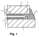
- Fig. 1 is a cross sectional view schematically illustrating the end portion in the side sealed structure of a flat display panel disclosed in Japanese Patent Laid-open Publication No. Hei 5-13003.
- a front plate 11 is formed of a glass substrate 1, and transparent electrodes 2 and transparent dielectric layers 3 formed thereon.
- a back plate 21 is formed of a glass substrate 4, and metal electrodes 5, black dielectric layers 6 and spacer ribs 7 formed thereon. The front plate 11 and the back plate 21 are arranged in parallel. The open sides of the spaced-plate structure are sealed with a fritted paste.
- the prior-art structure includes the spacer ribs 7 which maintain the gap between the front plate and the back plate to secure a discharge space.
- the spacer rib 7 is formed of, for example, a porous substance, not suitable for sealing, and is not used to seal the openings between the two plates.
- the thickness of the spacer rib 7 must be set to a value exceeding the total of the thickness of constituent elements formed on the glass substrate 1 and the thickness of the constituent elements formed on the glass substrate 4.
- the spacer rib 7 is formed of, for example, stacked films.
- the front plate and the back plate are spaced widely apart, and the opening area to be sealed with fritted glass 8 becomes large.
- the fritted glass 8 is in a paste state before its solidification through calcination.
- the fritted glass 8 is not supported in the opening area for sealing but holds its state by only its viscosity or surface tension against an external force such as gravity.
- the thickness of the fritted glass is prone to become uneven at the sealing portion.
- a large amount of fritted grass contains a large amount of solvent, The large amount of solvent permeating from the opening between a front plate and a back plate will contaminate the discharge space.
- two transparent insulating substrates are arranged in parallel so as to be spaced apart from each other.
- Plural linear discharge electrodes are arranged in parallel on each substrate.
- the linear electrodes on one substrate and the electrodes on the other substrate confront each other and are arranged in a matrix form.
- a partition wall defining a discharge space for each electrode is formed on the substrate.
- the display control is performed by selecting the confronting electrodes arranged in a matrix form. As a result, the display control cannot be independently performed for each display cell.
- the above-mentioned structure leads to a thick flat display panel.
- a flat display panel with a novel structure different from the conventional structure has been strongly desired to develop a flat display panel with a novel structure different from the conventional structure.
- the present applicant proposed a flat display panel with a new structure in the international application (PCT/JP98/01444) based on the Patent Cooperation Treaty.
- recessed portions each acting as a discharge space for a display cell, arranged in a matrix form are formed in the back plate.
- pairs of cell electrodes are formed on the regions confronting the recessed portions of the back plate.
- the front plate is disposed over the back plate.
- pin electrodes penetrate the back plate so that a voltage signal can be applied to a given spot of an electrode formed on the front plate.
- this structure allows a voltage to be applied between a pair of cell electrodes corresponding to a display cell so that the display cells can be respectively display-controlled. Since the back plate has recessed portions each for a discharge space, it is not required to attach or stack partition walls partitioning discharge spaces on the substrate, as shown in the prior art. Hence, this feature allows the display panel to be thinned.
- the flat display panel with this new structure differs from the conventional flat display panel using linear electrodes, in that cells can be respectively driven using pin electrodes.
- a large screen can be easily divided into plural flat display panels.
- a large screen can be easily fabricated by arranging panels each smaller than the conventional flat display panel. Additionally, a panel having defect pixels can be easily replaced with a new one.
- the objective of the invention is to provide a flat display panel with a novel structure in which the front panel is bonded with the back plate.
- Further objective of the invention is to provide a structure that can solve the above-mentioned problems in the conventional flat display panel.
- the flat display panel comprises a front panel of a transparent glass substrate on which cell electrode pairs are arranged for pixels, and a back plate having recessed portions formed in a surface thereof, the recessed portions being positioned so as to confront the cell electrode pairs, the recessed portions each defining a discharge space, the back plate being placed over the front plate; the back plate having a sealing wall having a top surface of the back plate remaining outside a display region formed of the recessed portions; the front plate having a protrusion protruding outward from the outer fringe of the sealing wall; wherein a contact portion between the sealing wall and the front plate is sealed by depositing a bonding agent in a corner portion defined by the outer side surface of the sealing wall and the protrusion of the front plate, the corner portion being adjacent to the bonding portion.
- At least the front plate or the back plate has a groove extending along the sealing wall in a plate surface region where the top surface of said sealing wall confronts the front plate.
- the flat display panel according to the present invention further comprises a barrier for blocking the bonding agent on the outer fringe portion of the front plate.
- a flat panel display comprises a front panel of a transparent glass substrate on which cell electrode pairs are arranged for pixels; and a back plate having recessed portions formed in a surface thereof, the recessed portions being positioned so as to confront the cell electrode pairs, the recessed portions each defining a discharge space, the back plate being placed over the front plate; the back plate having a sealing wall having a top surface of the back plate remaining outside a display region formed of the recessed portions; wherein a contact portion between the sealing wall and the front plate is sealed by means of a bonding agent layer to be bonded on the outer side surface of a superposed structure of the front plate and the back plate as well as a band member to be securely bonded on the outer side surface of the superposed structure pressure-bonded to the bonding agent layer.
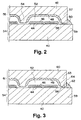
- Fig. 2 is a cross sectional view schematically illustrating a sealed side portion of a flat display panel with a novel structure according to the first embodiment of the present invention.
- This structure includes a transparent glass substrate 40 acting as a front plate and a glass substrate 42 acting as a back plate.
- a transparent electrode layer is deposited on the back surface of the transparent glass substrate (facing the back plate) and then cell electrodes 44 are formed by patterning the electrode layer.
- a pair of cell electrodes 44 are disposed for a pixel or cell.
- a dielectric layer 46 is formed over the cell electrodes 44 to electrically insulate them.
- Recessed portions 52 each called a cell for a pixel are formed in the glass substrate acting as the back plate.
- the cells are formed by depositing a mask layer on the surface of the glass substrate 42 and then sand-blasting the remaining regions except the mask region.
- Each recessed portion corresponds to a pixel and has a rectangular opening.
- a fluorescent layer 48 is coated on the inner surface of each recessed portion 52.
- the front plate 54 including a transparent glass substrate 40 acting as a base substrate is placed over the back plate 55 including a glass substrate 42 acting as a base substrate so as to cause cell electrodes 44 to respectively confront recessed portions 52.
- the glass substrate 42 is disposed so as to be adjacent to the surface of the front plate.
- a fixed discharge space is defined over the cell electrode 44 by the recessed portion 52 of the glass substrate 42.
- a glow discharge occurs within the discharge space by applying a voltage between cell electrodes 44.
- the glow discharge emits ultraviolet rays which irradiate the fluorescent substance layer 48.
- the fluorescent light emitted from the fluorescent substance layer 48 passes through the area confronting the front plate 54 and is then emitted from the surface of the transparent glass substrate 40.
- a partition wall 56 is the portion remained between the recessed portion 52 corresponding to each pixel.
- the partition wall 56 separates the discharge spaces of pixels from each other and allows the pixels to be respectively emitted.
- the partition wall has a notch which communicates gas between cells.
- the front plate 54 is combined with the back plate 55. The open sides of the two spaced plates are sealed (as described later). Then, the air is evacuated out of all the cells through the exhaust tube disposed at a portion of the intermediate structure. Then, Ne-Xe, for example, is injected into all the cells through the exhaust tube.
- the recessed portions 52 are formed in only the surfaces of the back plate 55 corresponding to display areas.
- the surfaces of the glass substrate 42 surrounding the display areas are not sculptured in the sand-blasting.
- the glass surface with high evenness is left between the edge of the glass substrate 42 and the outer fringe pixel.
- the narrow portion is formed all over the outer periphery of the glass substrate 42 and acts as the sealing wall 57 which hermetically seals cells formed in the inner area of the glass substrate from the outside.
- the width of the top of the sealing wall 57 defining the gap between the outer cells and the edge of glass substrate 42 is, for example, about 0.25 mm.
- the dead space occupied by the end portion of the flat display panel can be suppressed by thinning the width of the sealing wall 57.
- the gap between the top surface of the sealing wall 57, or the surface of the glass substrate 42, and the joint portion 58 of the front plate is as small as about 5 ⁇ m.
- the joint portion 58 is externally sealed with a sealing bonding agent such as fritted glass.
- the transparent glass substrate 40 has a protruding portion 59 protruding out from the outer periphery position of the sealing wall 57, or from the side surface of the glass substrate 42. In other words, the transparent glass substrate 40 is somewhat larger than the glass substrate 42.
- the fritted glass 50 are deposited at the corner defined by the top surface of the protruding portion 59 (corresponding to a back surface of the transparent glass substrate 40) and the outer side surface of the sealing wall 57 (corresponding to the side end surface of the glass substrate 42).
- the fritted glass paste invades into the gap at the joint portion 58. In such a situation, the fritted glass 50 is calcinated and solidified so that the open sides of the intermediate structure formed of the front paste 54 and the back plate 52 are hermetically sealed.
- the recessed portions 52 each acting as a cell formed in the glass substrate 42 can eliminate the spacer rib and reduce the gap between the front plate 54 and the back plate 55.
- the side walls of the recessed portions formed at the outer periphery work as the sealing wall 57.
- the sealing wall 57 being a part of the glass substrate 42 does not pass gas, unlike the porous spacer rib. Hence, the sealing is sufficiently accomplished simply by filling the vicinity of the narrowed joint portions 58 with the fritted glass 50. This means that excellent hermetic sealing can be maintained with a small amount of the fritted glass.
- the protrusion of the protruding portion 50 may be set to about 0.25 mm.
- the very small gap at the joint portion 58 decided by the flatness of the transparent glass substrate 40 and the flatness of the glass substrate 42 can prevent the solvent for fritted glass from leaking toward the cell.
- the portion where the spacer rib 7 is in contact with the glass substrate 1 in the conventional structure shown in Fig. 1 is sealed with a fritted glass. Since the porous spacer rib cannot maintain the hermetic state of the cell, the flatness of the top surface is lower than that of the glass substrate even if the spacer rib is made of a gas blocking substance, because the spacer rib is formed by stacking film substances. The portion may occur where the gap between the glass substrates 1 and the top surface of the rib becomes partially large. The portion with a large gap may introduce the fritted glass and the solvent into the discharge space. In contrast, the structure of the present embodiment does not have such a disadvantage.
- the transparent substrate 40 is exposed at the portion where the top surface of the sealing wall 57 is in contact with the front plate 54.
- the gap at the joint portion 58 can be easily and uniformly maintained at a small value.
- the dielectric layer 46 may extend to the portion where the sealing wall 57 contacts.
- the dielectric layer 46 may be formed all over the surface of the transparent glass substrate 40.
- the substance of the dielectric layer 46 and the substance smoothing step are considered to secure the flatness of the surface of the dielectric layer 46.
- the sealing wall which is defined by sculpturing a substrate forming a back plate, is jointed to the front plate.
- the joint portion is sealed with a bonding agent.
- the protruding portion protruding out from the sealing wall joint surface prevents a bonding agent from protruding out from the end of the font plate, so that the boundary between the display surfaces of neighbor panels becomes inconspicuous.
- the small gap between the sealing wall and the front plate requires a small amount of bonding agent, the size of the protruding portion becomes small.
- the dead space not used for displaying is effectively reduced.
- the small gap between the sealing wall and the front plate can effectively prevent the solvent for the bonding agent from penetrating into the discharge space.
- Fig. 3 is a cross sectional view schematically illustrating the end portion of a flat display panel with a new structure according to the second embodiment of the present invention.
- like numerals represent the same constituent elements as those in the first embodiment.
- the present structure differs from the structure in the above-mentioned embodiment in that a groove 64 is formed in the sealing wall 63 of the back plate 61 and along the sealing wall.
- the groove 64 is formed at the same time when the recessed portions 52 are formed in the glass substrate 60 in the sand-blasting step.
- the width of the groove 64 is, for example, about 100 to 150 ⁇ m. Because the mask opening is small in the sand blasting step, the depth of the groove 64 is, for example, about 100 to 300 ⁇ m smaller than the depth (e.g. about 600 ⁇ m) of the recessed portion.
- the thickness of the sealing wall 63 is about 0.25 mm, as shown in the above-mentioned embodiment.
- the back plate 61 including the glass substrate 60 with the groove 64 is placed over the front plate 54.
- the joint portion 58 between the sealing wall 63 and the front plate 54 is sealed with the fritted glass 62 deposited on the protruding portion 59.
- the groove 64 blocks the fritted glass invading the gap at the joint portion 58. In other words, the groove 64 prevents the fritted glass 62 from advancing through the joint portion 58 of the sealing wall 63 into the cell area. Thus, it can be avoided that the solvent for the fritted glass 62 pollutes the inside of the cell area.
- the groove 64 is formed in the back plate 61.
- This structure has the advantage that the groove 61 is formed at the same time in the sand blasting step, together with the recessed portions 52, and has another advantage that the front plate 54 is easily positioned with the back plate 61 by self-aligning the top surface of the sealing wall 63 with the groove 64.
- the structure where the groove 64 is formed in the top surface of the sealing wall 63 can be applied to the case where the portion of the transparent glass substrate 40 to which the sealing wall 63 adjoins is coated with the dielectric layer 46.
- the groove 64 may be formed in the portion of the transparent glass substrate 40 to which the sealing wall 63 adjoins. This structure requires another sand-blasting step but can prevent the fritted glass 62 from penetrating into the cell area.
- the front plate or back plate has a groove along the sealing wall and at the joint portion between the sealing wall and the front plate.
- This structure can maintain at a moderate value the amount that a bonding agent deposited outside the joint portion penetrates. That is, the bonding agent may easily invade the groove but is difficult to invade the inner area over the groove. Hence the disadvantages that the bonding agent reaches the discharge space and that the solvent for the bonding agent contaminates the same can be eliminated while the reliability of sealing is maintained.
- Fig. 4 is a cross-sectional view schematically illustrating the end of a flat display panel according to the third embodiment of the present invention.
- Like numerals represent the same constituent elements as those in the above-mentioned embodiments, and so duplicate description will be omitted here.
- the present structure differs from that in the first embodiment in that a barrier 70 of thin film glass is attached on the side surface of the protruding portion 59 of the transparent glass substrate 40 forming the front plate 54.
- the barrier 70 protrudes on the side where the fritted glass 72 for sealing the joint portion 58 is deposited.
- a ditch is defined by the side surface of the glass substrate 42, the top surface of the protruding portion of the transparent glass substrate 40, and the barrier 70 along the outside of the joint portion 58.
- the ditch is filled with the fritted glass 72.
- the structure blocks the fritted glass spreading outward from the surface of the substrate.
- flat display panels can be arranged so as to abut the side end surfaces of the transparent glass substrates 40 on each other. This feature enables the joint between flat panel displays to be viewed seamlessly from the front side thereof.
- the fritted glass substrate 40 does not overflow from the end of the transparent glass substrate 40, so that the panel periphery space not effectively used as a display area is reduced.
- the fritted glass 72 is vertically filled between the barrier 70 and the side surface of the glass substrate 42, that is, in the direction of the thickness of the panel. Since the contact area where the fritted glass 72 comes into contact with the side surface of the glass substrate 42 and the barrier 70 can be expanded, a high reliability hermetic seal can be secured.
- the flat display panel of the present invention has a barrier that blocks a bonding agent at the outer side surfaces of the front substrate.
- This barrier prevents the bonding agent sealing the joint portion defined between the front plate and the back plate from spreading outward from the outer side surfaces of the front plate.
- This structure has the advantage that since the gap between neighboring panels is small, the boundary on display panels becomes inconspicuous. Moreover, since the protruding portion of the front plate can be shortened, the dead space in displaying can be effectively reduced. The distance between the joint portion to be sealed with a bonding agent and the outer portion is extended by filling the space between the back plate and the barrier with a bonding agent. As a result, the hermetic reliability can be effectively improved.
- Fig. 5 is a cross sectional view schematically illustrating the end of the side sealing portion of a flat display panel with a new structure according to the fourth embodiment of the present invention.
- like numerals represent the same constituent elements as those in the above-mentioned embodiment.
- the present structure differs from that in the first embodiment in that the front plate 81 includes the transparent glass substrate 80 and has no protruding portion 59 protruding from the back plate 55 (or the glass substrate 82). That is, the back plate 55 is placed over the front plate 81 while the end surface of the back plate 56 is substantially flush with that of the front plate 81.
- the fritted glass is deposited on the outer side of the joint portion 58 between the sealing wall 57 and the transparent glass substrate 80.
- a metal band 86 is placed over the fritted glass 84 under pressure and the fritted glass 84 is then calcinated.
- the fritted glass 84 is squeezed along the side surface of the flat display panel by clamping the metal band 86. With such a condition sustained, the fritted glass is calcinated and solidified. Thus, the surface area of the fritted glass 84 exposed to air is reduced. The distance of the boundary between the side surface of the glass substrate 82 or the transparent glass substrate 80 and the surface of the fritted glass 84 becomes long, ranging from the end where the fritted glass is exposed to air to the joint portion 58. Hence, the cell area can be hermetically sealed with high reliability.
- the metal band 86 clamps the fritted glass 84 to prevent it from bulging in the direction of the panel main surface. This means that the gap between neighbor display panels can be reduced.
- the advantage is that the seam between panels is unobtrusively viewed from the main panel surface and that the waste area not used as a display area can be reduced.
- the metal band 86 is basically wounded over the whole side surface of the flat display panel.
- the metal band 86 may be formed of strips attached to the sides of the flat display panel and each having a length corresponding to that of each of the sides thereof.
- the metal band 86 may be formed of two L-shaped metal plates disposed so as to surround the flat display panel. Each L-shaped metal plate may be formed of strips previously jointed and corresponding to two neighboring sides.
- the metal band 86 may be a rectangular metal frame fitting the outer shape of the flat display panel. The superposed structure of the front plate 81 and the back plate 55 may be inserted into the rectangular frame.
- the thickness of the metal band 86 is as thin as possible.
- the metal band 86 has a thickness of 0.1 to 0.2 mm.
- the glass substrates 80 and 82 will expand and contract in the step of calcinating the fritted glass 84 or due to changes in temperature of the flat display panel in use.
- the metal band 86 is of a material with a thermal expansion coefficient close to that of the glass material. The use of such a material can prevent occurrence of stress due to differences in thermal expansion or contraction between the glass substrate 82 and the metal band 86, and peeling of the metal band 86 due to the stress, and sealing degradation due to the peeling.
- 50NiFe (with a linear expansion coefficient of 94 ⁇ 10 -7 deg -1 ) is used for a soda glass substrate (with a linear expansion coefficient of 85 ⁇ 10 -7 deg -1 ).
- Tungsten (W) (with a linear expansion coefficient of 46 ⁇ 10 -7 deg -1 ) or molybdenum (M) (with a linear expansion coefficient of 51 ⁇ 10 -7 deg -1 ) or 29NiFeCo (kover) (with a linear expansion coefficient of 45 ⁇ 10 -7 deg -1 ) is used for a non-alkali glass substrate (with a linear expansion coefficient of 45 to 50 ⁇ 10 -7 deg -1 ).
- a band member is rolled over the bonding agent deposited at the joint portion between the front plate and the back plate.
- the band member spreads the bonding agent over the side surface of a flat display panel.
- the surface area that the bonding agent has exposed to the air is reduced.
- the distance between the outside air and the joint portion between the front plate and the back plate and over which the bonding area is sealed with the bonding agent is made longer, so that the cell area can be hermetically sealed with high reliability.
- the band member rolls the bonding agent layer, thus preventing the bonding agent from bulging in the direction of the main panel surface.
- the gap between neighbor display panels can be narrowed so that the boundary between display panels becomes inconspicuous.
- the dead space in displaying can be reduced due to no protruding portion.
Landscapes
- Engineering & Computer Science (AREA)
- Physics & Mathematics (AREA)
- Plasma & Fusion (AREA)
- Manufacturing & Machinery (AREA)
- Gas-Filled Discharge Tubes (AREA)
- Manufacture Of Electron Tubes, Discharge Lamp Vessels, Lead-In Wires, And The Like (AREA)
Applications Claiming Priority (2)
| Application Number | Priority Date | Filing Date | Title |
|---|---|---|---|
| JP27519598 | 1998-09-29 | ||
| JP27519598A JP3442294B2 (ja) | 1998-09-29 | 1998-09-29 | 平面表示パネル |
Publications (2)
| Publication Number | Publication Date |
|---|---|
| EP0991098A2 true EP0991098A2 (de) | 2000-04-05 |
| EP0991098A3 EP0991098A3 (de) | 2000-04-12 |
Family
ID=17552017
Family Applications (1)
| Application Number | Title | Priority Date | Filing Date |
|---|---|---|---|
| EP99106696A Withdrawn EP0991098A3 (de) | 1998-09-29 | 1999-04-01 | Flache Anzeigetafel |
Country Status (6)
| Country | Link |
|---|---|
| US (1) | US6528944B1 (de) |
| EP (1) | EP0991098A3 (de) |
| JP (1) | JP3442294B2 (de) |
| KR (1) | KR100334169B1 (de) |
| CN (1) | CN1249526A (de) |
| TW (1) | TW442818B (de) |
Cited By (3)
| Publication number | Priority date | Publication date | Assignee | Title |
|---|---|---|---|---|
| US6746294B1 (en) * | 2000-08-07 | 2004-06-08 | Mitsubishi Denki Kabushiki Kaisha | Method for fabricating a flat, light-emitting display panel |
| EP1760751A2 (de) | 2005-08-30 | 2007-03-07 | Samsung SDI Co., Ltd. | Plasmaanzeigetafel |
| EP2296164A3 (de) * | 2009-09-14 | 2011-08-10 | Canon Kabushiki Kaisha | Verbindungsverfahren aus Basismaterialien und Herstellungsverfahren einer Bildanzeigevorrichtung |
Families Citing this family (18)
| Publication number | Priority date | Publication date | Assignee | Title |
|---|---|---|---|---|
| CN100382224C (zh) * | 1996-12-16 | 2008-04-16 | 松下电器产业株式会社 | 气体放电屏及其制造方法 |
| JP2001189136A (ja) * | 1999-10-19 | 2001-07-10 | Matsushita Electric Ind Co Ltd | プラズマディスプレイ表示装置とその製造方法 |
| TW525118B (en) * | 2000-05-12 | 2003-03-21 | Acer Display Tech Inc | Plasma display having driving circuit mounted on single face and its manufacturing method |
| KR100445954B1 (ko) * | 2000-08-07 | 2004-08-25 | 미쓰비시덴키 가부시키가이샤 | 평면형 발광 표시 패널의 제조 방법 |
| US20030153233A1 (en) * | 2001-01-29 | 2003-08-14 | Yoshifumi Amano | Front side glass substrate for display and display device |
| KR100499129B1 (ko) * | 2002-09-02 | 2005-07-04 | 삼성전기주식회사 | 발광 다이오드 및 그 제조방법 |
| JP2004146211A (ja) * | 2002-10-24 | 2004-05-20 | Noritake Co Ltd | 平板型表示装置およびその封着方法 |
| KR100851470B1 (ko) * | 2002-12-05 | 2008-08-08 | 오리온피디피주식회사 | 플라즈마 디스플레이 패널 및 이를 이용한 멀티디스플레이패널 |
| KR100868413B1 (ko) | 2002-12-27 | 2008-11-11 | 오리온피디피주식회사 | 멀티형 플라즈마 디스플레이 패널 |
| TWI273322B (en) * | 2004-11-24 | 2007-02-11 | Coretronic Corp | Backlight module |
| KR101201305B1 (ko) * | 2005-06-28 | 2012-11-14 | 엘지디스플레이 주식회사 | 평판 표시 장치 및 이의 제조 방법 |
| TWI281684B (en) * | 2005-08-10 | 2007-05-21 | Ind Tech Res Inst | Anode plate structure for flat panel light source of field emission |
| KR100751369B1 (ko) * | 2006-03-06 | 2007-08-22 | 삼성에스디아이 주식회사 | 플라즈마 디스플레이 패널 |
| JP4791321B2 (ja) * | 2006-10-19 | 2011-10-12 | 国立大学法人 東京大学 | 表示装置の製造方法 |
| WO2008139508A1 (ja) * | 2007-05-10 | 2008-11-20 | Hitachi, Ltd. | プラズマディスプレイパネル |
| CN101789350A (zh) * | 2009-12-31 | 2010-07-28 | 四川虹欧显示器件有限公司 | 平板显示器及其制作方法 |
| US10057999B2 (en) | 2016-05-24 | 2018-08-21 | Microsoft Technology Licensing, Llc | Electronic device having a reduced dead border |
| TWI836963B (zh) * | 2023-04-13 | 2024-03-21 | 達擎股份有限公司 | 顯示裝置 |
Citations (1)
| Publication number | Priority date | Publication date | Assignee | Title |
|---|---|---|---|---|
| US5626772A (en) * | 1995-03-20 | 1997-05-06 | Philips Electronics North America Corporation | Plasma addressed liquid crystal display with etched plasma channels |
Family Cites Families (14)
| Publication number | Priority date | Publication date | Assignee | Title |
|---|---|---|---|---|
| US3975725A (en) * | 1973-12-26 | 1976-08-17 | Burroughs Corporation | Display panel and system for operating the same |
| US4139250A (en) * | 1975-10-27 | 1979-02-13 | U.S. Philips Corporation | Gas discharge display panel and method of manufacturing the same |
| NL8003697A (nl) * | 1980-06-26 | 1982-01-18 | Philips Nv | Werkwijze voor het vervaardigen van een elektrische ontladingsinrichting voorzien van een op een glazen substraat aangebracht elektrodenpatroon en aldus verkregen elektrische ontladingsinrichting. |
| JPS59110946A (ja) | 1982-12-14 | 1984-06-27 | Ricoh Co Ltd | 歯車装置 |
| US4853590A (en) * | 1988-08-01 | 1989-08-01 | Bell Communications Research, Inc. | Suspended-electrode plasma display devices |
| JPH0290192A (ja) | 1988-09-27 | 1990-03-29 | Nec Corp | 表示装置 |
| JPH0394751A (ja) | 1989-09-07 | 1991-04-19 | Toshiro Takashima | 介護ベット装置 |
| US5239228A (en) * | 1990-07-02 | 1993-08-24 | Sharp Kabushiki Kaisha | Thin-film electroluminescence device for displaying multiple colors with groove for capturing adhesive |
| JPH0513003A (ja) | 1991-07-04 | 1993-01-22 | Nec Corp | プラズマデイスプレイパネル |
| KR940010842B1 (ko) * | 1991-10-26 | 1994-11-17 | 삼성전관 주식회사 | 플라즈마 어드레스 방식의 액정표시소자 |
| JP2593761B2 (ja) * | 1992-02-06 | 1997-03-26 | 株式会社ノリタケカンパニーリミテド | プラズマディスプレイパネル |
| JPH09507958A (ja) | 1994-11-04 | 1997-08-12 | オリオン・エレクトリック・カンパニー・リミテッド | プラズマディスプレイパネル |
| US5959403A (en) * | 1996-10-09 | 1999-09-28 | Lg Electronics Inc. | Plasma display panel with magnetic partition walls |
| US6323596B1 (en) | 1997-03-31 | 2001-11-27 | Mitsubishi Denki Kabushiki Kaisha | Planar display panel and panel manufacturing method |
-
1998
- 1998-09-29 JP JP27519598A patent/JP3442294B2/ja not_active Expired - Fee Related
-
1999
- 1999-03-04 US US09/262,090 patent/US6528944B1/en not_active Expired - Fee Related
- 1999-03-05 TW TW088103405A patent/TW442818B/zh not_active IP Right Cessation
- 1999-03-05 KR KR1019990007233A patent/KR100334169B1/ko not_active Expired - Fee Related
- 1999-04-01 EP EP99106696A patent/EP0991098A3/de not_active Withdrawn
- 1999-06-08 CN CN99108402A patent/CN1249526A/zh active Pending
Patent Citations (1)
| Publication number | Priority date | Publication date | Assignee | Title |
|---|---|---|---|---|
| US5626772A (en) * | 1995-03-20 | 1997-05-06 | Philips Electronics North America Corporation | Plasma addressed liquid crystal display with etched plasma channels |
Cited By (5)
| Publication number | Priority date | Publication date | Assignee | Title |
|---|---|---|---|---|
| US6746294B1 (en) * | 2000-08-07 | 2004-06-08 | Mitsubishi Denki Kabushiki Kaisha | Method for fabricating a flat, light-emitting display panel |
| EP1760751A2 (de) | 2005-08-30 | 2007-03-07 | Samsung SDI Co., Ltd. | Plasmaanzeigetafel |
| EP1760751A3 (de) * | 2005-08-30 | 2008-08-27 | Samsung SDI Co., Ltd. | Plasmaanzeigetafel |
| EP2296164A3 (de) * | 2009-09-14 | 2011-08-10 | Canon Kabushiki Kaisha | Verbindungsverfahren aus Basismaterialien und Herstellungsverfahren einer Bildanzeigevorrichtung |
| US8429935B2 (en) | 2009-09-14 | 2013-04-30 | Canon Kabushiki Kaisha | Bonding method of base materials, and manufacturing method of image display apparatus |
Also Published As
| Publication number | Publication date |
|---|---|
| CN1249526A (zh) | 2000-04-05 |
| KR20000022589A (ko) | 2000-04-25 |
| US6528944B1 (en) | 2003-03-04 |
| TW442818B (en) | 2001-06-23 |
| JP3442294B2 (ja) | 2003-09-02 |
| KR100334169B1 (ko) | 2002-04-25 |
| JP2000106093A (ja) | 2000-04-11 |
| EP0991098A3 (de) | 2000-04-12 |
Similar Documents
| Publication | Publication Date | Title |
|---|---|---|
| US6528944B1 (en) | Flat panel display with reduced display dead space | |
| JPH0812348B2 (ja) | プラズマアドレス方式の液晶表示素子とその製造方法 | |
| US5800232A (en) | Plasma-addressed display panel and a method of manufacturing the same | |
| US5684361A (en) | Plasma discharge chamber arrangement for plasma-addressed display device | |
| US5834896A (en) | Plasma display with barrier ribs | |
| KR100371259B1 (ko) | 플라즈마어드레스표시장치및그제조방법 | |
| JPH0513003A (ja) | プラズマデイスプレイパネル | |
| JP3750239B2 (ja) | 画像表示装置 | |
| KR19980063952A (ko) | 플라즈마 어드레스 전기 광학 표시 장치 | |
| JP3301277B2 (ja) | プラズマアドレス表示装置 | |
| KR100723089B1 (ko) | 플라즈마 표시패널 | |
| JP3782347B2 (ja) | 平面型表示装置およびその製造方法 | |
| JP3840750B2 (ja) | 画像表示装置の製造方法 | |
| KR100736259B1 (ko) | 플라즈마 표시패널 | |
| KR20010000978A (ko) | 플라즈마 표시판넬의 제조방법 | |
| KR101029146B1 (ko) | 플라즈마 표시패널 | |
| KR19980076919A (ko) | 칼라 플라즈마 디스플레이 패널의 유(u)자형 전극 형성방법 | |
| KR20010000980A (ko) | 플라즈마 표시판넬의 제조방법 | |
| KR100228573B1 (ko) | 소형 fed용 패키지 | |
| US20060119268A1 (en) | Plasma display panel and manufacturing method thereof | |
| KR100212734B1 (ko) | 평판표시소자 및 그 제조방법 | |
| JPH08304790A (ja) | プラズマアドレス表示装置の製造方法 | |
| JPH06250158A (ja) | プラズマアドレス表示装置の製造方法 | |
| KR19990017002A (ko) | 칼라 플라즈마 디스플레이 패널 | |
| JP2003288852A (ja) | 発光型表示装置の前面側ガラス基板の構造 |
Legal Events
| Date | Code | Title | Description |
|---|---|---|---|
| PUAI | Public reference made under article 153(3) epc to a published international application that has entered the european phase |
Free format text: ORIGINAL CODE: 0009012 |
|
| PUAL | Search report despatched |
Free format text: ORIGINAL CODE: 0009013 |
|
| AK | Designated contracting states |
Kind code of ref document: A2 Designated state(s): DE FR GB |
|
| AX | Request for extension of the european patent |
Free format text: AL;LT;LV;MK;RO;SI |
|
| AK | Designated contracting states |
Kind code of ref document: A3 Designated state(s): AT BE CH CY DE DK ES FI FR GB GR IE IT LI LU MC NL PT SE |
|
| AX | Request for extension of the european patent |
Free format text: AL;LT;LV;MK;RO;SI |
|
| 17P | Request for examination filed |
Effective date: 20000510 |
|
| AKX | Designation fees paid |
Free format text: DE FR GB |
|
| 17Q | First examination report despatched |
Effective date: 20020315 |
|
| STAA | Information on the status of an ep patent application or granted ep patent |
Free format text: STATUS: THE APPLICATION IS DEEMED TO BE WITHDRAWN |
|
| 18D | Application deemed to be withdrawn |
Effective date: 20050628 |