EP0991124A2 - Reseau de mémoire DRAM avec quatre cellules pour chaque contact de ligne de bit - Google Patents
Reseau de mémoire DRAM avec quatre cellules pour chaque contact de ligne de bit Download PDFInfo
- Publication number
- EP0991124A2 EP0991124A2 EP99116439A EP99116439A EP0991124A2 EP 0991124 A2 EP0991124 A2 EP 0991124A2 EP 99116439 A EP99116439 A EP 99116439A EP 99116439 A EP99116439 A EP 99116439A EP 0991124 A2 EP0991124 A2 EP 0991124A2
- Authority
- EP
- European Patent Office
- Prior art keywords
- wordlines
- semiconductor memory
- recited
- cell
- capacitors
- Prior art date
- Legal status (The legal status is an assumption and is not a legal conclusion. Google has not performed a legal analysis and makes no representation as to the accuracy of the status listed.)
- Withdrawn
Links
Images


Classifications
-
- H—ELECTRICITY
- H10—SEMICONDUCTOR DEVICES; ELECTRIC SOLID-STATE DEVICES NOT OTHERWISE PROVIDED FOR
- H10B—ELECTRONIC MEMORY DEVICES
- H10B12/00—Dynamic random access memory [DRAM] devices
- H10B12/30—DRAM devices comprising one-transistor - one-capacitor [1T-1C] memory cells
- H10B12/34—DRAM devices comprising one-transistor - one-capacitor [1T-1C] memory cells the transistor being at least partially in a trench in the substrate
-
- H—ELECTRICITY
- H10—SEMICONDUCTOR DEVICES; ELECTRIC SOLID-STATE DEVICES NOT OTHERWISE PROVIDED FOR
- H10B—ELECTRONIC MEMORY DEVICES
- H10B12/00—Dynamic random access memory [DRAM] devices
-
- H—ELECTRICITY
- H10—SEMICONDUCTOR DEVICES; ELECTRIC SOLID-STATE DEVICES NOT OTHERWISE PROVIDED FOR
- H10B—ELECTRONIC MEMORY DEVICES
- H10B12/00—Dynamic random access memory [DRAM] devices
- H10B12/01—Manufacture or treatment
- H10B12/02—Manufacture or treatment for one transistor one-capacitor [1T-1C] memory cells
-
- H—ELECTRICITY
- H10—SEMICONDUCTOR DEVICES; ELECTRIC SOLID-STATE DEVICES NOT OTHERWISE PROVIDED FOR
- H10B—ELECTRONIC MEMORY DEVICES
- H10B12/00—Dynamic random access memory [DRAM] devices
- H10B12/30—DRAM devices comprising one-transistor - one-capacitor [1T-1C] memory cells
-
- H—ELECTRICITY
- H10—SEMICONDUCTOR DEVICES; ELECTRIC SOLID-STATE DEVICES NOT OTHERWISE PROVIDED FOR
- H10B—ELECTRONIC MEMORY DEVICES
- H10B12/00—Dynamic random access memory [DRAM] devices
- H10B12/30—DRAM devices comprising one-transistor - one-capacitor [1T-1C] memory cells
- H10B12/48—Data lines or contacts therefor
- H10B12/488—Word lines
-
- H—ELECTRICITY
- H10—SEMICONDUCTOR DEVICES; ELECTRIC SOLID-STATE DEVICES NOT OTHERWISE PROVIDED FOR
- H10D—INORGANIC ELECTRIC SEMICONDUCTOR DEVICES
- H10D84/00—Integrated devices formed in or on semiconductor substrates that comprise only semiconducting layers, e.g. on Si wafers or on GaAs-on-Si wafers
- H10D84/80—Integrated devices formed in or on semiconductor substrates that comprise only semiconducting layers, e.g. on Si wafers or on GaAs-on-Si wafers characterised by the integration of at least one component covered by groups H10D12/00 or H10D30/00, e.g. integration of IGFETs
- H10D84/82—Integrated devices formed in or on semiconductor substrates that comprise only semiconducting layers, e.g. on Si wafers or on GaAs-on-Si wafers characterised by the integration of at least one component covered by groups H10D12/00 or H10D30/00, e.g. integration of IGFETs of only field-effect components
- H10D84/83—Integrated devices formed in or on semiconductor substrates that comprise only semiconducting layers, e.g. on Si wafers or on GaAs-on-Si wafers characterised by the integration of at least one component covered by groups H10D12/00 or H10D30/00, e.g. integration of IGFETs of only field-effect components of only insulated-gate FETs [IGFET]
- H10D84/834—Integrated devices formed in or on semiconductor substrates that comprise only semiconducting layers, e.g. on Si wafers or on GaAs-on-Si wafers characterised by the integration of at least one component covered by groups H10D12/00 or H10D30/00, e.g. integration of IGFETs of only field-effect components of only insulated-gate FETs [IGFET] comprising FinFETs
-
- H—ELECTRICITY
- H10—SEMICONDUCTOR DEVICES; ELECTRIC SOLID-STATE DEVICES NOT OTHERWISE PROVIDED FOR
- H10D—INORGANIC ELECTRIC SEMICONDUCTOR DEVICES
- H10D1/00—Resistors, capacitors or inductors
- H10D1/40—Resistors
- H10D1/47—Resistors having no potential barriers
-
- Y—GENERAL TAGGING OF NEW TECHNOLOGICAL DEVELOPMENTS; GENERAL TAGGING OF CROSS-SECTIONAL TECHNOLOGIES SPANNING OVER SEVERAL SECTIONS OF THE IPC; TECHNICAL SUBJECTS COVERED BY FORMER USPC CROSS-REFERENCE ART COLLECTIONS [XRACs] AND DIGESTS
- Y10—TECHNICAL SUBJECTS COVERED BY FORMER USPC
- Y10S—TECHNICAL SUBJECTS COVERED BY FORMER USPC CROSS-REFERENCE ART COLLECTIONS [XRACs] AND DIGESTS
- Y10S257/00—Active solid-state devices, e.g. transistors, solid-state diodes
- Y10S257/905—Plural dram cells share common contact or common trench
Definitions
- Dram cell size is always of present concern as pressures continue to develop denser memories. Present design dictates that word lines and bitlines run perpendicular one another and that memory cells are arranged in pairs of two therewith sharing one bitline stud used to contact of the both memory cells with a bitline.
- Figure 1 illustrates a top view and partial schematic of a conventional trench DRAM memory cell layout and figure 2 illustrates a 3-dimensional , partial cross-sectional drawing of a layout according to figure 1.
- Each pair memory cells is associated with two trench capacitors 1 and two active access consisting of drain (source) and buried strap 2 and gate 3 is associated with one BL stud and one drain (source) region 4 below.
- wordlines 5 are running over the active accsess decives forming the gates of the devices therewith.
- the bitline studs are connected to respective bit lines 6 , BL n , where n is integer running on a second metal level perpendicular to the wordlines.
- the dimensions of a memory cell are commonly defined by the smallest feature size defined in fabricating the memory cell. Typically, the smallest feature size is equal to the width of the memory cell gate.
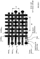
- Figure 3 illustrates a top view of the invention's DRAM cell layout which provides a 6 1 ⁇ 4 f 2 DRAM cell structure with four nodes (cells) per bitline-stud and two topological wordline levels.
- Bit line (BL) stud and drain/source region 10 are shown in the center of 4 cells each associated with a cell capacitor 7 shown with circular top-down view cross-section.
- Drain/source buried strap 8 connects capacitor 7 with a drain/source of its respective memory cell.
- Gates 9 are shown between associated drain/source regions 8 and 10 along with respective buried straps and BL studs.
- Four gates share a common BL stud and drain/source region 10 which serves to connect shared drain/source regions associated with the four gates and with bitlines 13 .
- Each four gate structure shall be referenced as a cell-quadropole and indicated generally by reference number 15 .
- 0.15 micron minimum feature size 0.1406... ( ⁇ m) 2 surface area is occupied by the layout of the present invention, a smaller amount than the 0.18 ( ⁇ m) 2 surface area of the 8f 2 conventional cell.
- the more compact size also dictates a slightly different bitline and wordline orientation.
- some wordlines run parallel to bit lines, the conductors which provide access to the memory cells for the input and output of information to the cell during READ and WRITE cycles and during REFRESH, an operation which periodically restores cell information to compensate for capacitor leakage.
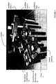
- Figure 4 illustrates a three-dimensional, partial cross-sectional drawing of the layout of the present invention using a cell capacitor implemented as a trench capacitor. Many of the elements (wordlines and bitlines) in figure 4 are shown truncated along a plane for ease of illustration of the structure.
- Trench capacitor 7 extends down into the chip substrate and is shown here as being of a cylindrical shape. This illustration of capacitor 7 is for example only. Alternatively, capacitor 7 is contemplated as a stacked capacitor or some combination of trench and stacked capacitor.
- Wordlines on metal level 0 (referred to as wordlines level 0) 11 , two of which are shown in figure 3 as wordline n and wordline n+1 , (wherein n, here and throughout represents a whole number) respectively, connected to two of the gates 9 in each four node structure 15 , run parallel to bit lines 13 (two of which are shown as bitline n and bitline n+1 , respectively) in metal level 2 which are connected through a via hole to each respective bit line stud and drain/source region 10 below.
- Wordlines on a second metal level 1 (referred to as wordlines level 1) 12 service the remaining two cells among each four node structure (or quadropole) 15 and vias (also referred to as wordline studs 14 ) are used to connect the gates 9 to the wordlines 12 in the metal 1 level with studs similar to the bitline stud 4 .
- Wordlines 12 in metal 1 (as indicated by WL n+ 2 and WL n+3 ) run perpendicular to wordlines 11 in metal level 0.
- the bitlines 13 may run parallel (as used in the description above) or perpendicular to wordlines 11 in metal level 0.
- bitlines can be fabricated on a metal level also used in conventional memory design.
- the foregoing described DRAM cell structure can be fabricated as follows as shown in those figures: A silicon wafer is processed by a series of process steps beginning with the formation of a plurality of trench capacitors 8 using deep trench (DT) etch, DT poly-Si fill and DT poly chemical-mechanical polishing (CMP) etc. in a layout as shown in figure 3.
- the fill of the trench capacitor serves as one electrode, the Si bulk with certain implanted layers as the other.
- These process steps are well known to those skilled in the art and may contain further process steps like the creation of buried plates, outdiffusions, multiple-step re-etch and re-fills, collar-sidewall oxidation, anneal steps etc for the actual manufacturing of trench capacitors.
- the trench capacitors 8, created by the aforementioned processing, are connected via a buried strap 10 to active devices formed in a cross-shaped transistor active area (AA) region.
- the AA regions are isolated against each other by surrounding shallow trench isolation (STI) regions.
- the aforementioned metal layers may be created by using reactive ion etch (RIE) techniques as well as by using Damascene techniques.
- RIE reactive ion etch
- a Si-oxide layer is grown which will later act as gate oxide.
- a thin Si 3 N 4 layer is deposited.
- a third possibly thicker layer of boron-doped phospho-silicate glass (BPSG) is deposited. In to this BPSG layer holes are etched at the position of all gates 9 which will be created later.
- the previously deposited Si 3 N 4 layer acts as etch stop.
- the photo-resist exposure is performed in such a manner that the diameter of the holes is slightly smaller than one feature size, f, and such that the four holes per quadropole don't touch each other.
- the Si 3 N 4 on the bottom of the created holes is removed in order to expose the gate oxide.
- Poly-Si is then deposited into the holes with a thickness which is small compared to the diameter of the holes. The remaining BPSG and Si 3 N 4 is removed. Consequently, small cylinders from poly-Si have been fabricated forming the gates.
- CMOS complementary metal-oxide-semiconductor
- FETs field effect transistors
- BPSG deposited between the Si-gate-cylinders and a CMP process is performed to obtain a planar surface for further process steps.
- GC gate conductor
- the GC stacks may contain layers from poly-Si, WSi 2 and Si 3 N 4 as common in the fabrication of DRAMs. These level zero wordlines 11 or GC stacks are covered with a thin insolating protective layer possibly consisting of nitride. Further deposition of a thick isolating layer, typically BPSG, creates an isolating fill and cover of the level zero wordlines 11 .
- Wordline level one 12 may again consist of different layers of conducting and or non-conducting material. Crucial however is again a thin protective film covering wordline level one.
- a thick isolating layer made from BPSG or TEOS
- wordline level one 12 Similar to the steps described before for wordline level zero 11 a final etch in the center of each quatrupole structure down to the Si-wafer surface is made.
- the adjacent wordlines 11 , 12 and wordline-studs 14 are protected from exposure by the before mentioned protective layer.
- additional biasing during photo-resist exposure for the last etch step may be applied to reduce the diameter of the hole and ensure an etch without damage on the before created structures.
- bitline stud which reaches up to the bitlines 13 which are finally created on top of the described two levels of wordlines 11 and 12 running parallel to wordline level zero 11 .
- processing of further wiring structures may be performed as know and typical for back-end-of-line (BEOL) processing.
Landscapes
- Engineering & Computer Science (AREA)
- Manufacturing & Machinery (AREA)
- Semiconductor Memories (AREA)
Applications Claiming Priority (2)
| Application Number | Priority Date | Filing Date | Title |
|---|---|---|---|
| US163670 | 1988-03-03 | ||
| US09/163,670 US6188095B1 (en) | 1998-09-30 | 1998-09-30 | 6¼ f2 DRAM cell structure with four nodes per bitline-stud and two topological wordline levels |
Publications (2)
| Publication Number | Publication Date |
|---|---|
| EP0991124A2 true EP0991124A2 (fr) | 2000-04-05 |
| EP0991124A3 EP0991124A3 (fr) | 2005-12-14 |
Family
ID=22591060
Family Applications (1)
| Application Number | Title | Priority Date | Filing Date |
|---|---|---|---|
| EP99116439A Withdrawn EP0991124A3 (fr) | 1998-09-30 | 1999-08-21 | Reseau de mémoire DRAM avec quatre cellules pour chaque contact de ligne de bit |
Country Status (6)
| Country | Link |
|---|---|
| US (1) | US6188095B1 (fr) |
| EP (1) | EP0991124A3 (fr) |
| JP (1) | JP2000114496A (fr) |
| KR (1) | KR20000023521A (fr) |
| CN (1) | CN1225027C (fr) |
| TW (1) | TW464871B (fr) |
Cited By (1)
| Publication number | Priority date | Publication date | Assignee | Title |
|---|---|---|---|---|
| DE102006048587A1 (de) * | 2006-09-22 | 2008-04-03 | Qimonda Ag | Speicherarray und Verfahren zum Herstellen eines Speicherarrays |
Families Citing this family (17)
| Publication number | Priority date | Publication date | Assignee | Title |
|---|---|---|---|---|
| US6331733B1 (en) | 1999-08-10 | 2001-12-18 | Easic Corporation | Semiconductor device |
| US6667502B1 (en) * | 1999-08-31 | 2003-12-23 | Micron Technology, Inc. | Structurally-stabilized capacitors and method of making of same |
| US6570211B1 (en) * | 2002-06-26 | 2003-05-27 | Advanced Micro Devices, Inc. | 2Bit/cell architecture for floating gate flash memory product and associated method |
| KR100866710B1 (ko) * | 2002-07-18 | 2008-11-03 | 주식회사 하이닉스반도체 | 반도체 소자의 워드라인 형성 방법 |
| US6727540B2 (en) * | 2002-08-23 | 2004-04-27 | International Business Machines Corporation | Structure and method of fabricating embedded DRAM having a vertical device array and a bordered bitline contact |
| KR100539276B1 (ko) | 2003-04-02 | 2005-12-27 | 삼성전자주식회사 | 게이트 라인을 포함하는 반도체 장치 및 이의 제조 방법 |
| US7161226B2 (en) * | 2003-10-20 | 2007-01-09 | Industrial Technology Research Institute | Multi-layered complementary wire structure and manufacturing method thereof |
| JP2005285971A (ja) * | 2004-03-29 | 2005-10-13 | Nec Electronics Corp | 半導体装置 |
| US7501676B2 (en) * | 2005-03-25 | 2009-03-10 | Micron Technology, Inc. | High density semiconductor memory |
| US8310859B2 (en) | 2008-09-30 | 2012-11-13 | Samsung Electronics Co., Ltd. | Semiconductor memory device having balancing capacitors |
| JP5653001B2 (ja) * | 2009-03-16 | 2015-01-14 | ピーエスフォー ルクスコ エスエイアールエルPS4 Luxco S.a.r.l. | 半導体装置及び半導体装置の補償容量の配置方法 |
| US8872344B2 (en) | 2010-06-09 | 2014-10-28 | Texas Instruments Incorporated | Conductive via structures for routing porosity and low via resistance, and processes of making |
| KR101119038B1 (ko) * | 2011-06-01 | 2012-03-16 | 주식회사 오킨스전자 | 적층구조를 갖는 반도체 패키지 지지장치 |
| US10834611B1 (en) * | 2019-09-05 | 2020-11-10 | International Business Machines Corporation | Network availability notification in predefined travel scenarios |
| CN113451270B (zh) | 2020-03-25 | 2023-12-05 | 长鑫存储技术有限公司 | 位线结构和半导体存储器 |
| CN113451269B (zh) | 2020-03-25 | 2022-07-22 | 长鑫存储技术有限公司 | 字线结构和半导体存储器 |
| KR102744282B1 (ko) | 2020-08-03 | 2024-12-19 | 에스케이하이닉스 주식회사 | 반도체 장치 및 반도체 장치의 제조 방법 |
Family Cites Families (9)
| Publication number | Priority date | Publication date | Assignee | Title |
|---|---|---|---|---|
| JPH03188668A (ja) * | 1989-12-18 | 1991-08-16 | Mitsubishi Electric Corp | 半導体記憶装置 |
| JPH03278573A (ja) * | 1990-03-28 | 1991-12-10 | Mitsubishi Electric Corp | 半導体記憶装置 |
| JP2824713B2 (ja) * | 1992-04-24 | 1998-11-18 | 三菱電機株式会社 | 半導体記憶装置 |
| US5838038A (en) * | 1992-09-22 | 1998-11-17 | Kabushiki Kaisha Toshiba | Dynamic random access memory device with the combined open/folded bit-line pair arrangement |
| JPH07202022A (ja) * | 1993-12-28 | 1995-08-04 | Nippon Steel Corp | 半導体記憶装置 |
| JPH08227982A (ja) * | 1994-11-14 | 1996-09-03 | Nippon Steel Corp | 高密度半導体記憶装置 |
| US5770874A (en) * | 1994-11-14 | 1998-06-23 | Nippon Steel Corporation | High density semiconductor memory device |
| KR100190522B1 (ko) * | 1995-06-09 | 1999-06-01 | 김영환 | 반도체 메모리 집적회로 및 그 제조방법 |
| JP2950265B2 (ja) * | 1996-07-30 | 1999-09-20 | 日本電気株式会社 | 半導体記憶装置 |
-
1998
- 1998-09-30 US US09/163,670 patent/US6188095B1/en not_active Expired - Lifetime
-
1999
- 1999-08-21 EP EP99116439A patent/EP0991124A3/fr not_active Withdrawn
- 1999-09-29 KR KR1019990041695A patent/KR20000023521A/ko not_active Withdrawn
- 1999-09-29 TW TW088116719A patent/TW464871B/zh not_active IP Right Cessation
- 1999-09-30 JP JP11280142A patent/JP2000114496A/ja active Pending
- 1999-09-30 CN CNB991208501A patent/CN1225027C/zh not_active Expired - Fee Related
Cited By (1)
| Publication number | Priority date | Publication date | Assignee | Title |
|---|---|---|---|---|
| DE102006048587A1 (de) * | 2006-09-22 | 2008-04-03 | Qimonda Ag | Speicherarray und Verfahren zum Herstellen eines Speicherarrays |
Also Published As
| Publication number | Publication date |
|---|---|
| CN1225027C (zh) | 2005-10-26 |
| JP2000114496A (ja) | 2000-04-21 |
| TW464871B (en) | 2001-11-21 |
| KR20000023521A (ko) | 2000-04-25 |
| EP0991124A3 (fr) | 2005-12-14 |
| CN1267090A (zh) | 2000-09-20 |
| US6188095B1 (en) | 2001-02-13 |
Similar Documents
| Publication | Publication Date | Title |
|---|---|---|
| US5497017A (en) | Dynamic random access memory array having a cross-point layout, tungsten digit lines buried in the substrate, and vertical access transistors | |
| US6188095B1 (en) | 6¼ f2 DRAM cell structure with four nodes per bitline-stud and two topological wordline levels | |
| US6426526B1 (en) | Single sided buried strap | |
| US6537870B1 (en) | Method of forming an integrated circuit comprising a self aligned trench | |
| US6184549B1 (en) | Trench storage dynamic random access memory cell with vertical transfer device | |
| KR100641943B1 (ko) | 반도체 칩용으로 워드라인 측벽에 인접하여 형성되는 수직형 장치 및 그 제조 방법 | |
| KR100643425B1 (ko) | 수직형 트랜지스터 및 매립된 워드라인을 갖는 반도체 디바이스 | |
| JP2002094027A (ja) | 半導体記憶装置とその製造方法 | |
| JP2003017585A (ja) | 半導体記憶装置およびその製造方法 | |
| JPH04212450A (ja) | 半導体記憶装置およびその製造方法 | |
| KR20000006064A (ko) | 반도체 집적회로장치 및 그 제조방법 | |
| JP2003031686A (ja) | 半導体記憶装置およびその製造方法 | |
| US5714401A (en) | Semiconductor device capacitor manufactured by forming stack with multiple material layers without conductive layer therebetween | |
| US6638812B2 (en) | Method for producing a memory cell for a semiconductor memory | |
| US6181014B1 (en) | Integrated circuit memory devices having highly integrated SOI memory cells therein | |
| US6566219B2 (en) | Method of forming a self aligned trench in a semiconductor using a patterned sacrificial layer for defining the trench opening | |
| JP3305932B2 (ja) | 半導体装置およびその製造方法 | |
| JP3177038B2 (ja) | 半導体記憶装置及びその製造方法 | |
| HK1023650A (en) | Dram memory array with four cells per bit line contact | |
| JP3147163B2 (ja) | 半導体装置およびその製造方法 | |
| JPH1079490A (ja) | 半導体記憶装置のコンデンサ構造体 | |
| JP2001185692A (ja) | 半導体装置の製造方法と半導体装置 | |
| KR100456313B1 (ko) | 매립형 비트라인의 제조 방법 | |
| US6369418B1 (en) | Formation of a novel DRAM cell | |
| KR960014970B1 (ko) | 반도체기억장치 및 그 제조방법 |
Legal Events
| Date | Code | Title | Description |
|---|---|---|---|
| PUAI | Public reference made under article 153(3) epc to a published international application that has entered the european phase |
Free format text: ORIGINAL CODE: 0009012 |
|
| AK | Designated contracting states |
Kind code of ref document: A2 Designated state(s): AT BE CH CY DE DK ES FI FR GB GR IE IT LI LU MC NL PT SE |
|
| AX | Request for extension of the european patent |
Free format text: AL;LT;LV;MK;RO;SI |
|
| RAP1 | Party data changed (applicant data changed or rights of an application transferred) |
Owner name: INFINEON TECHNOLOGIES AG |
|
| PUAL | Search report despatched |
Free format text: ORIGINAL CODE: 0009013 |
|
| AK | Designated contracting states |
Kind code of ref document: A3 Designated state(s): AT BE CH CY DE DK ES FI FR GB GR IE IT LI LU MC NL PT SE |
|
| AX | Request for extension of the european patent |
Extension state: AL LT LV MK RO SI |
|
| 17P | Request for examination filed |
Effective date: 20060427 |
|
| AKX | Designation fees paid |
Designated state(s): DE FR GB IE IT |
|
| REG | Reference to a national code |
Ref country code: HK Ref legal event code: WD Ref document number: 1023650 Country of ref document: HK |
|
| 17Q | First examination report despatched |
Effective date: 20080806 |
|
| STAA | Information on the status of an ep patent application or granted ep patent |
Free format text: STATUS: THE APPLICATION IS DEEMED TO BE WITHDRAWN |
|
| 18D | Application deemed to be withdrawn |
Effective date: 20090217 |