EP0991210B1 - Doppelseitenbandpilottechnik eines Kontrollsystems für Reduktion die durch die elektrische Schaltung generierte Verzerrung - Google Patents
Doppelseitenbandpilottechnik eines Kontrollsystems für Reduktion die durch die elektrische Schaltung generierte Verzerrung Download PDFInfo
- Publication number
- EP0991210B1 EP0991210B1 EP99307452A EP99307452A EP0991210B1 EP 0991210 B1 EP0991210 B1 EP 0991210B1 EP 99307452 A EP99307452 A EP 99307452A EP 99307452 A EP99307452 A EP 99307452A EP 0991210 B1 EP0991210 B1 EP 0991210B1
- Authority
- EP
- European Patent Office
- Prior art keywords
- circuit
- electrical circuit
- frequency
- side band
- control system
- Prior art date
- Legal status (The legal status is an assumption and is not a legal conclusion. Google has not performed a legal analysis and makes no representation as to the accuracy of the status listed.)
- Expired - Lifetime
Links
- 238000000034 method Methods 0.000 title description 6
- 238000001514 detection method Methods 0.000 claims description 23
- 230000003595 spectral effect Effects 0.000 description 2
- 230000001360 synchronised effect Effects 0.000 description 2
- 238000012935 Averaging Methods 0.000 description 1
- 230000002411 adverse Effects 0.000 description 1
- 230000003111 delayed effect Effects 0.000 description 1
- 230000001419 dependent effect Effects 0.000 description 1
- 230000000694 effects Effects 0.000 description 1
- 230000003993 interaction Effects 0.000 description 1
- 230000002452 interceptive effect Effects 0.000 description 1
- 230000000644 propagated effect Effects 0.000 description 1
Images


Classifications
-
- G—PHYSICS
- G05—CONTROLLING; REGULATING
- G05B—CONTROL OR REGULATING SYSTEMS IN GENERAL; FUNCTIONAL ELEMENTS OF SUCH SYSTEMS; MONITORING OR TESTING ARRANGEMENTS FOR SUCH SYSTEMS OR ELEMENTS
- G05B11/00—Automatic controllers
- G05B11/01—Automatic controllers electric
- G05B11/26—Automatic controllers electric in which the output signal is a pulse-train
- G05B11/30—Automatic controllers electric in which the output signal is a pulse-train using pulse-frequency modulation
-
- H—ELECTRICITY
- H03—ELECTRONIC CIRCUITRY
- H03F—AMPLIFIERS
- H03F1/00—Details of amplifiers with only discharge tubes, only semiconductor devices or only unspecified devices as amplifying elements
- H03F1/32—Modifications of amplifiers to reduce non-linear distortion
- H03F1/3223—Modifications of amplifiers to reduce non-linear distortion using feed-forward
- H03F1/3229—Modifications of amplifiers to reduce non-linear distortion using feed-forward using a loop for error extraction and another loop for error subtraction
- H03F1/3235—Modifications of amplifiers to reduce non-linear distortion using feed-forward using a loop for error extraction and another loop for error subtraction using a pilot signal
-
- H—ELECTRICITY
- H03—ELECTRONIC CIRCUITRY
- H03F—AMPLIFIERS
- H03F2201/00—Indexing scheme relating to details of amplifiers with only discharge tubes, only semiconductor devices or only unspecified devices as amplifying elements covered by H03F1/00
- H03F2201/32—Indexing scheme relating to modifications of amplifiers to reduce non-linear distortion
- H03F2201/3212—Using a control circuit to adjust amplitude and phase of a signal in a signal path
Definitions
- the present invention is directed to a control system comprising an electrical circuit that uses a pilot signal to substantially cancel distortion produced by the electrical circuit and more particularly to a technique of applying a double side band pilot signal at the edges of the band of operation of the electrical circuit.
- a well known technique for substantially canceling distortion produced by an electrical circuit uses a control system coupled to the electrical circuit to which a pilot signal is applied.
- the applied pilot signal is detected by the control system.
- the applied pilot signal can have a single spectral component (i.e., one frequency) of a certain amplitude or the applied pilot signal can comprise a plurality of spectral components of various amplitudes.
- the applied pilot signal has an amplitude that is at least 60 dB lower than signals applied to or generated by the electrical circuit.
- the control system obtains information (about the distortion) from the detected pilot signal and uses that information to substantially cancel the distortion produced by the electrical circuit.
- a control system comprises at least one circuit which uses external signals or signals generated by the at least one circuit to process signals applied to the at least one circuit.
- FIG. 1 depicts a control system, comprising two feed forward loops (loop 1 and loop 2) and detection circuit 132.
- a pilot signal is applied to electrical circuit 108 via coupler 105.
- Electrical circuit 108 can be any electrical and/or electronic (e.g., Radio Frequency (RF) linear amplifier, power amplifier) circuit.
- Loop 1 comprises coupler 105, Gain & Phase circuit 104, splitter 102 and delay circuit 126.
- Coupler 105 is typically a device which combines two or more input signals and allows access to all or a portion of the combined signal.
- a coupler is also used to obtain a portion of a signal appearing at its input and output.
- Gain & Phase circuit 104 is typically a circuit which modifies the amplitude and phase of signals applied to its input based on the values of control signals applied to its control inputs (not shown).
- Splitter 102 is a circuit with one input and at least two outputs where a signal applied to the input is substantially replicated at the outputs.
- Delay circuit 126 is typically a circuit which applies a certain amount of delay to a signal applied to its input.
- splitter 102 When a signal is applied to the input of the control system (i.e., to splitter 102), the distortion experienced by the applied signal due to electrical circuit 108 is isolated at point A (i.e., path 123).
- an input signal is applied to splitter 102.
- Splitter 102 substantially replicates the input signal on paths 103 and 127.
- path 103 the input signal is applied to Gain & Phase circuit 104, coupler 105 and electrical circuit 108.
- path 127 the input signal is delayed by delay circuit 126 and then fed to cancellation circuit 124 via path 125.
- the amplitude and phase of the input signal on path 125 can be detected (using well known detection circuitry) and converted to control signals that are applied to the control inputs (not shown) of Gain and Phase circuit 104.
- coupler 112 a portion of the input signal (plus any distortion produced by electrical circuit 108) appearing at the output of electrical circuit 108 is fed to cancellation circuit 124 via path 113.
- Cancellation circuit 124 can be implemented as a combiner circuit which has at least two inputs and one output. A combiner circuit combines signals applied to its inputs and transfers the combined signal to its output.
- Gain and Phase circuit 104 is adjusted such that the amplitude and phase of the input signal on path 113 are modified resulting in that signal being substantially 180° out of phase (+/- 1°) and relatively the same amplitude (i.e., substantially the inverse) with the input signal on path 125 such that when the two signals are combined by cancellation circuit 124 they substantially cancel each other leaving the distortion (produced by electrical circuit 108) at point A (path 123).
- Loop 1 is designed to isolate the distortion produced by electrical circuit 108.
- Loop 2 which comprises delay circuit 114, coupler 116, Gain & Phase circuit 122, and amplifier 120, is designed to use information obtained by Detection circuit 132 from a pilot signal applied to electrical circuit 108 to substantially cancel the distortion produced by electrical circuit 108.
- a pilot signal is applied to electrical circuit 108 via coupler 105.
- the pilot signal (processed by electrical circuit 108) appears on path 115 and at the output of coupler 116, i.e., on path 117.
- the pilot signal also appears at point A on path 123 after having propagated through path 113 via coupler 112.
- a portion of the pilot signal processed by electrical circuit 108 is fed to detection circuit 132 via coupler 130 and path 128.
- Detection circuit 132 comprises well known circuits (e.g., Log detector/amplifier, Sample & Hold circuit, Null circuit) to detect signal characteristics (e.g., amplitude) of the pilot signal. Some or all of the characteristics may have been altered due to the distortion effects of electrical circuit 108. Detection circuit 132 detects the characteristics of the input and uses this information to generate control signals on path 131 to cause Gain & Phase circuit 122 to modify the pilot signal. The pilot signal at point A is modified such that the pilot signal appearing on path 118 is substantially the inverse (relatively same amplitude, 180° out of phase, +/- 1°) of the pilot signal appearing on path 115. Amplifier 120 provides additional gain to the output of Gain & Phase circuit 122.
- Signal characteristics e.g., amplitude
- the additional gain is calculated such that the signal appearing on path 118 has an amplitude substantially equal to the amplitude of the signal on path 115.
- Delay circuit 114 is designed such that the two pilot signals arrive at coupler 116 at substantially the same moment; that is, the two pilot signals are substantially synchronized (aligned in time) to each other. When the two pilot signals are combined by coupler 116 they cancel each other.
- Detection circuit 132 now has the information that allows Gain & Phase circuit 122 to modify distortion appearing at point A and thus cancel distortion appearing at the output of electrical circuit 108.
- any distortion produced by electrical circuit 108 is isolated at point A (on path 123) as discussed above.
- the signal on path 115 is the input signal (processed by electrical circuit 108) plus any distortion produced by electrical circuit 108.
- the distortion at point A is modified by Gain and Phase circuit 122 based on the information (i.e., signal characteristics) obtained from the previously applied pilot signal so that the distortion on path 129 is substantially the inverse of the distortion on path 115.
- the distortions on path 115 and path 118 are combined at coupler 116 causing the distortions to substantially cancel each other resulting in an output signal that is substantially free of distortion.
- Electrical circuit 108 has a bandwidth that defines a frequency band of operation. It is desirable that the pilot signal be spectrally located substantially in the middle of the frequency band of operation of electrical circuit 108 because the distortion experienced by such a pilot signal tends to be substantially similar to the distortion experienced by a signal applied to or generated by electrical circuit 108. However, placing the pilot signal anywhere in the band of operation of electrical circuit 108 causes interference to occur between the input signal and the pilot signal adding more distortion to the input signal. The interference is any interaction between the pilot signal and an applied or generated signal that adversely affects one or more characteristic (e.g., amplitude, frequency, phase) of the applied or generated signal and/or the pilot signal.
- a characteristic e.g., amplitude, frequency, phase
- interference not only distorts any signal that is applied or generated by the electrical circuit, but also affects the pilot signal.
- the pilot signal is typically 60 dB below the amplitude of applied or generated signals and thus would be interfered with by such signals.
- a distorted pilot signal provides inaccurate information about the distortion and thus the very purpose of such a pilot signal is defeated.
- the pilot signal is located in the middle of the frequency band of operation, it does not experience the distortions located in other parts (e.g., lower band or upper band) of the frequency band of operation. What is therefore needed is to use a pilot signal that obtains information about the entire frequency band of operation of the electrical circuit and does so without interfering with any signals applied to or generated by the electrical circuit.
- the present invention is a control system comprising an electrical circuit that produces distortion where the electrical circuit has a frequency band of operation.
- the side bands of a carrier signal spectrally located proximate to the boundaries of the frequency band of operation are used as pilot signals and are applied to the electrical circuit.
- Information about the distortion is obtained from the side band pilot signals which do not interfere with any signal applied to or generated within the frequency band of operation of the electrical circuit. The information obtained is used by the control system to substantially cancel the distortion produced by the electrical circuit.
- the control system of the present invention also comprises a first feed forward loop and a second feed forward loop coupled to the electrical circuit.
- the control system of the present invention further comprises a Carrier circuit coupled to a Double Side Band (DSB) modulator which is coupled to the electrical circuit.
- the control system of the present invention still further comprises a Detection circuit coupled to the carrier circuit and the second feed forward loop.
- the Carrier circuit is configured to generate a carrier signal.
- the DSB modulator is configured to generate side band pilot signals spectrally located outside the band of operation of the electrical circuit.
- the side band pilot signals are created from a carrier having a center frequency corresponding to the center frequency of the electrical circuit modulated by a signal whose frequency component is equal to more than half the bandwidth of the electrical circuit.
- the Detection circuit obtains information about the distortion produced by the electrical circuit from the side band pilot signals and provides the information to the second feed forward loop.
- the first feed forward loop is configured to isolate the distortion produced by the electrical circuit.
- the second feed forward loop is configured to use the information obtained by the Detection circuit to substantially cancel the distortion produced by the electrical circuit.
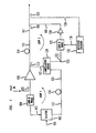
- a control system of the present invention comprising electrical circuit 108 coupled to a first feed forward loop (i.e., loop 1) and a second feed loop (i.e., loop 2).
- the control system of the present invention further comprises Carrier circuit 156 coupled to Double Side Band (DSB) modulator 154 and to Detection circuit180.
- Electrical circuit 108 produces distortion which is isolated at point A by loop 1.
- Loop 2 uses information obtained from the Detection circuit 180 to cancel the distortion produced by electrical circuit 108.
- Detection Circuit 180 The information obtained by Detection Circuit 180 is gleaned from double side band pilot signals (i.e., two pilot signals) applied to electrical circuit 108 (via path 146 and couple 105) with the use of carrier circuit 156 and DSB modulator 154.
- Carrier circuit 156 along with DSB modulator 154 generate the pilot signals from which Detection circuit 180 obtains information.
- the pilot signals are spectrally located outside of the frequency band of operation of electrical circuit 108 and thus do not to interfere with any signal applied or generated within the frequency band of electrical circuit 108.
- the pilot side bands are created by modulating a carrier whose frequency is equal to the center frequency of the bandwidth of electrical circuit 108 with a signal whose frequency is equal to more than half the bandwidth of electrical circuit 108.
- the frequency response is a chart or graph showing how a particular characteristic (e.g., amplitude, phase) of an electrical circuit corresponds with frequency. It should be noted that the particular frequency response shown is for illustrative purposes only and that electrical circuit 108 is not limited to frequency response 300.
- the frequency band of operation is a range of frequencies within each element circuit 108 processes and/or generates signals. The boundaries of the frequency band of operation are defined by lower frequency f L and upper frequency f U .
- Frequencies f L and f U correspond to the points (304, 306) at which the frequency response is 3 dB below its maximum amplitude response (o dB).
- the bandwidth of a circuit is defined by the frequencies that correspond to its 3 dB points.
- the frequency band of operation need not be the bandwidth.
- Frequency f 0 is defined as the center frequency of the bandwidth of electrical circuit 108.
- Side band pilot signals 306 and 308 can be located at the 3 dB frequencies or preferably, as shown in FIG.
- the side band pilot signals are preferably located outside the frequency band of operation but proximate to the boundaries of the frequency band of operation. Proximate location of the side band pilot signals is defined as frequencies about the frequency band of operation which allow the pilot signals to provide information that are used to substantially cancel the distortion produced by electrical circuit 108.
- Carrier circuit 156 comprises Oscillator 158 coupled to Splitter 160.
- Each of the outputs of Splitter 160 is coupled to an amplifier (162, 184).
- One of the outputs is applied to Mixer 172 of Detection Circuit 180 and the other output is applied to DSB modulator 154.
- Oscillator 158 generates a carrier (i.e., a sinusoid) whose frequency is equal to the center frequency, f 0 (305) of electrical 108.
- DSB modulator 154 is a well known circuit shown here comprising Oscillator 150 and mixer 148.
- Oscillator 150 generates a modulating signal (i.e., a sinusoid) of a certain frequency preferably equal to more than half the bandwidth of electrical circuit 108.
- the output of Oscillator 150 is coupled to an output of Carrier to one input of mixer 148.
- the other input of mixer 148 is coupled to an output of Carrier circuit 156.
- Carrier circuit 156 comprises oscillator 158 coupled to splitter 160 having two outputs each of which is connected to an amplifier (162, 184).
- Oscillator 158 of Carrier circuit 156 generates a carrier whose frequency is preferably equal to the center frequency (f 0 ) of the bandwidth of electrical circuit 108.
- the output of DSB modulator 154 is the carrier signal modulated with the modulating signal which results in two signals commonly referred to as side bands.
- the frequency of one side band is equal to the sum of the carrier frequency and the modulating frequency.
- the frequency of the other side band is equal to the difference of the carrier frequency and the modulating frequency. Therefore, when the carrier frequency is f 0 and the frequency of the modulating signal is equal to slightly more than half the bandwidth of electrical circuit 108 then the side bands are located proximate to the 3 dB frequencies (f L , f U ) of electrical circuit 108.
- the modulating frequency can be selected to be any frequency and thus the side bands can be located within or without the frequency band of operation.
- the frequency of the modulating signal is selected such that the side bands are located outside the bandwidth but proximate to the 3 dB frequencies or outside of the frequency band of operation of electrical circuit 108 but proximate to the boundaries of the frequency band of operation.
- the side bands are used as pilot signals which are applied to electrical circuit 108 via amplifier 144, path 146 and coupler 105.
- the pilot signals appear on path 117 and portions of the pilot signals are coupled to path 128 via coupler 130 and applied to Detection circuit 180.
- Detection circuit 180 comprises BSF 168 coupled to amplifier 170 coupled to Mixer 172 which is coupled BPF 174.
- Detection circuit 180 further comprises Log Detector 176 coupled to BPF 174 and to LPF 178.
- the pilot modulated carrier signal is applied to Band Stop Filter (BSF) 168 of Detection circuit 180.
- BSF 168 is a filter circuit that rejects or significantly attenuates signals having certain frequencies and does not affect all other signals.
- BSF 168 is designed to reject any signal falling within the band of operation of electrical circuit 108.
- the pilot signals are then applied to Mixer 172 via amplifier 170.
- An output of carrier circuit 156 is also applied to Mixer 172.
- Mixer 172 is a well known circuit having at least two inputs and at least one output where the output is the result of the two input signals being multiplied to each other. It is well known that when two signals having certain frequencies are mixed, the result are signals comprising frequencies which are the sum and difference of the frequencies of the two signals.
- the mixing of two signals having the same frequencies is known as synchronous detection. Therefore, the pilot signals are synchronously detected by Mixer 172 and the output of Mixer 172 is fed to BPF 174 whose center frequency is equal to the frequency of Oscillator 150. The output of BPF 174 is therefore the pilot signal.
- the pilot signal is applied to Log Detector 176 which detects a characteristic (e.g., amplitude) of the pilot signal and converts said characteristic to a voltage.
- the output of Log Detector 176 is applied to Low Pass Filter (LPF) 178.
- LPF 178 acts as an averaging circuit and generates an average of a characteristic (e.g., amplitude) of the detected pilot signal which contains information about the distortion experienced by the pilot signal.
- the average is applied to Null circuit 132 via path 136.
- Null circuit 132 generates a control signal to Gain & Phase circuit 122 via path 131.
- the control signals generated by Null circuit 132 cause Gain & Phase amplifier 122 to modify the distortion at point A such that it is canceled with distortion appearing on path 115 with the use of coupler 116.
Landscapes
- Physics & Mathematics (AREA)
- Engineering & Computer Science (AREA)
- Nonlinear Science (AREA)
- Power Engineering (AREA)
- General Physics & Mathematics (AREA)
- Automation & Control Theory (AREA)
- Amplifiers (AREA)
- Stereo-Broadcasting Methods (AREA)
- Monitoring And Testing Of Transmission In General (AREA)
- Cable Transmission Systems, Equalization Of Radio And Reduction Of Echo (AREA)
- Noise Elimination (AREA)
Claims (4)
- Ein Regelsystem mit einer elektrischen Schaltung (108), welche eine Verzerrung erzeugt und ein von Grenzen (304, 306) definiertes Betriebsband, eine erste Vorwärtsschleife (loop 1), welche an die elektrische Schaltung gekoppelt ist, wobei die erste Vorwärtsschleife die Verzerrung ermittelt, und eine zweite Vorwärtsschleife (loop 2), welche an die erste Vorwärtsschleife gekoppelt ist, um im Wesentlichen die Verzerrung aufzuheben, aufweist, wobei das Regelsystem GEKENNZEICHNET IST DURCH: Einen Doppelseitenband-Modulator (154), welcher an einen Eingang der elektrischen Schaltung und an die zweite Vorwärtsschleife gekoppelt ist, wobei der Doppeiseitenband-Moduiator Seitenband-Pilotsignale (306, 308) erzeugt, indem er ein Trägersignal moduliert, dessen Frequenz der Mittenfrequenz der Bandbreite der Schaltung entspricht, welche an den Eingang der elektrischen Schaltung angelegt werden und spektral außerhalb des Betriebsfrequenzband der elektrischen Schaltung liegen, um die Verzerrungseigenschaften, welche von der zweiten Vorwärtsschleife im Wesentlichen zum Aufheben der Verzerrung verwendet werden, zu ermitteln, wobei die Bandbreite von den 3 dB-Punkten des Frequenzgangs der Schaltung definiert wird und das Betriebsband von der oberen und der unteren Betriebsfrequenz der Schaltung definiert wird, wobei das besagte Betriebsband Frequenzen umfasst, welche nicht in der Bandbreite enthalten sind.
- Das Regelsystem nach Anspruch 1, weiterhin umfassend eine Detektionsschaltung (180), welche an den Doppelseitenband-Modulator und an die zweite Vorwärtsschleife gekoppelt ist, wobei die Detektionsschaltung Informationen von den Doppelseitenband-Pilotsignalen, welche an der elektrischen Schaltung angelegt sind, erhält und die Informationen an die zweite Vorwärtsschleife bereitstellt.
- Das Regelsystem nach Anspruch 1, wobei der Doppelseitenband-Modulator einen Oszillator (158) umfasst, welcher an einen Mischer (172) mit einem ersten und einem zweiten Ausgang gekoppelt ist, wobei der erste Ausgang an den Oszillator und der zweite Ausgang an eine Trägerschaltung, welche einen Trägeroszillator umfasst, gekoppelt ist.
- Das Regelsystem nach Anspruch 3, wobei der Oszillator der Trägerschaltung eine Sinuskurve, deren Frequenz der Mittenfrequenz der elektrischen Schaltung entspricht, erzeugt, und der Oszillator des Doppelseitenband-Modulator eine Modulationssinuskurve mit einer derartigen Frequenz erzeugt, dass, wenn die Sinuskurven vom Mischer des Doppelseitenband-Modulators gemischt werden, die sich daraus ergebenden Seitenband-Pilotsignale spektral außerhalb des Betriebsfrequenzbands liegen.
Applications Claiming Priority (2)
| Application Number | Priority Date | Filing Date | Title |
|---|---|---|---|
| US162553 | 1988-03-01 | ||
| US09/162,553 US6157254A (en) | 1998-09-29 | 1998-09-29 | Double side band pilot technique for a control system that reduces distortion produced by electrical circuits |
Publications (3)
| Publication Number | Publication Date |
|---|---|
| EP0991210A2 EP0991210A2 (de) | 2000-04-05 |
| EP0991210A3 EP0991210A3 (de) | 2003-05-07 |
| EP0991210B1 true EP0991210B1 (de) | 2009-11-25 |
Family
ID=22586123
Family Applications (1)
| Application Number | Title | Priority Date | Filing Date |
|---|---|---|---|
| EP99307452A Expired - Lifetime EP0991210B1 (de) | 1998-09-29 | 1999-09-21 | Doppelseitenbandpilottechnik eines Kontrollsystems für Reduktion die durch die elektrische Schaltung generierte Verzerrung |
Country Status (9)
| Country | Link |
|---|---|
| US (1) | US6157254A (de) |
| EP (1) | EP0991210B1 (de) |
| JP (1) | JP4209051B2 (de) |
| KR (1) | KR100719779B1 (de) |
| CN (1) | CN1116736C (de) |
| AU (1) | AU764149B2 (de) |
| BR (1) | BR9904247A (de) |
| CA (1) | CA2279444C (de) |
| DE (1) | DE69941660D1 (de) |
Families Citing this family (15)
| Publication number | Priority date | Publication date | Assignee | Title |
|---|---|---|---|---|
| US6411644B1 (en) * | 1998-09-29 | 2002-06-25 | Lucent Technologies Inc. | Frequency hop pilot technique for a control system that reduces distortion produced by electrical circuits |
| JP3533351B2 (ja) * | 1999-12-28 | 2004-05-31 | 日本無線株式会社 | フィードフォワード増幅器及びその制御回路 |
| US6320461B1 (en) * | 2000-05-12 | 2001-11-20 | Jhong Sam Lee | Ultra-linear feedforward RF power amplifier |
| JP2002101138A (ja) * | 2000-09-26 | 2002-04-05 | Toshiba Corp | フィードフォワード型リニアライザ |
| US6525603B1 (en) * | 2001-01-05 | 2003-02-25 | Remec, Inc. | Feedforward amplifier linearization adapting off modulation |
| US7436900B2 (en) * | 2001-03-28 | 2008-10-14 | Lucent Technologies Inc. | Intermodulation distortion identification and quantization circuit for a linear amplifier system |
| US6734726B2 (en) * | 2001-06-29 | 2004-05-11 | Remec, Inc. | Balanced distortion reduction circuit |
| EP1289128B1 (de) * | 2001-08-21 | 2010-11-10 | Panasonic Corporation | Vorwärtsgekoppelter Verstärker und Verfahren zum vorwärtsgekoppelten Verstärken |
| US6919764B2 (en) * | 2003-03-11 | 2005-07-19 | Andrew Corporation | Amplifier control system with statistical enhancement of resolution of digital control signals |
| JP4431325B2 (ja) * | 2003-05-26 | 2010-03-10 | 株式会社日立国際電気 | 増幅装置 |
| KR20080052085A (ko) * | 2006-12-07 | 2008-06-11 | 한국전자통신연구원 | 크기 차동 위상 편이 변조 장치 및 그 방법 |
| CN101145860B (zh) * | 2007-07-06 | 2010-09-08 | 哈尔滨工程大学 | 实时校正信道相位幅度的装置 |
| FR2924542B1 (fr) | 2007-11-29 | 2010-01-01 | Lpa Concepts | Amplificateur hf large bande comportant un systeme de reduction de distorsion et procede de reduction de distorsion associe |
| JP5593609B2 (ja) * | 2008-12-23 | 2014-09-24 | 日本電気株式会社 | 歪補償回路と歪補償方法と通信装置 |
| JP6280697B2 (ja) * | 2013-05-27 | 2018-02-14 | サイプレス セミコンダクター コーポレーション | パワーアンプ装置及びその補償方法 |
Family Cites Families (10)
| Publication number | Priority date | Publication date | Assignee | Title |
|---|---|---|---|---|
| JP2945451B2 (ja) * | 1990-07-25 | 1999-09-06 | 日本電信電話株式会社 | フィードフォワード増幅器 |
| JP3171924B2 (ja) * | 1992-05-28 | 2001-06-04 | 富士通株式会社 | フィードフォワード増幅器 |
| JP3367745B2 (ja) * | 1994-04-05 | 2003-01-20 | 株式会社東芝 | 歪補償器 |
| JPH0856126A (ja) * | 1994-08-10 | 1996-02-27 | Kokusai Electric Co Ltd | 歪補償増幅回路 |
| JP3361657B2 (ja) * | 1995-07-20 | 2003-01-07 | 松下電器産業株式会社 | フィードフォワード増幅器の制御装置および制御方法 |
| JP2917904B2 (ja) * | 1996-04-15 | 1999-07-12 | 日本電気株式会社 | フィードフォワード増幅器 |
| US5796304A (en) * | 1996-04-24 | 1998-08-18 | Powerwave Technologies, Inc. | Broadband amplifier with quadrature pilot signal |
| US5774018A (en) * | 1996-09-18 | 1998-06-30 | Hughes Electronics Corporation | Linear amplifier system and method |
| US5926067A (en) * | 1998-09-29 | 1999-07-20 | Lucent Technologies Inc. | Sweep pilot technique for a control system that reduces distortion produced by electrical circuits |
| US5986499A (en) * | 1998-12-21 | 1999-11-16 | Lucent Technologies Inc. | Pilot signal detection system using band reject filter |
-
1998
- 1998-09-29 US US09/162,553 patent/US6157254A/en not_active Expired - Fee Related
-
1999
- 1999-07-30 CA CA002279444A patent/CA2279444C/en not_active Expired - Fee Related
- 1999-09-20 BR BR9904247-9A patent/BR9904247A/pt not_active IP Right Cessation
- 1999-09-21 EP EP99307452A patent/EP0991210B1/de not_active Expired - Lifetime
- 1999-09-21 DE DE69941660T patent/DE69941660D1/de not_active Expired - Lifetime
- 1999-09-22 AU AU48859/99A patent/AU764149B2/en not_active Ceased
- 1999-09-27 JP JP27205999A patent/JP4209051B2/ja not_active Expired - Fee Related
- 1999-09-28 CN CN99120768A patent/CN1116736C/zh not_active Expired - Fee Related
- 1999-09-29 KR KR1019990041779A patent/KR100719779B1/ko not_active Expired - Fee Related
Also Published As
| Publication number | Publication date |
|---|---|
| EP0991210A3 (de) | 2003-05-07 |
| CN1116736C (zh) | 2003-07-30 |
| DE69941660D1 (de) | 2010-01-07 |
| CN1250251A (zh) | 2000-04-12 |
| BR9904247A (pt) | 2001-01-16 |
| EP0991210A2 (de) | 2000-04-05 |
| JP4209051B2 (ja) | 2009-01-14 |
| CA2279444C (en) | 2005-11-29 |
| JP2000124839A (ja) | 2000-04-28 |
| US6157254A (en) | 2000-12-05 |
| CA2279444A1 (en) | 2000-03-29 |
| AU4885999A (en) | 2000-03-30 |
| KR20000023530A (ko) | 2000-04-25 |
| AU764149B2 (en) | 2003-08-14 |
| KR100719779B1 (ko) | 2007-05-21 |
Similar Documents
| Publication | Publication Date | Title |
|---|---|---|
| EP0991210B1 (de) | Doppelseitenbandpilottechnik eines Kontrollsystems für Reduktion die durch die elektrische Schaltung generierte Verzerrung | |
| US6081156A (en) | Method and apparatus for amplifying feedforward linear power using pilot tone hopping | |
| US5926067A (en) | Sweep pilot technique for a control system that reduces distortion produced by electrical circuits | |
| JPH0265429A (ja) | 局部発振器フィードスルー消去回路 | |
| EP0991183B1 (de) | Pilottechnik mit Frequenzsprüngen für ein Steuersystem zur Reduzierung von Verzerrungen, die durch elektrische Schaltungen hervorgerufen werden | |
| US6094096A (en) | Pilot detection for a control system that reduces distortion produced by electrical circuits | |
| US6545487B1 (en) | System and method for producing an amplified signal with reduced distortion | |
| JP3080188B2 (ja) | フィードフォワード干渉回路 | |
| US7064608B2 (en) | Feed-forward-back suppressed noise circuits | |
| EP0980137A1 (de) | Synchrone Pilottondetektiontechnik für Steuerungssystem zur Reduzierung der durch elektrische Schaltungen erzeugten Entzerrung | |
| MXPA98010437A (en) | Improved pilot detection for a control system that reduces distortion produced by electri circuits |
Legal Events
| Date | Code | Title | Description |
|---|---|---|---|
| PUAI | Public reference made under article 153(3) epc to a published international application that has entered the european phase |
Free format text: ORIGINAL CODE: 0009012 |
|
| AK | Designated contracting states |
Kind code of ref document: A2 Designated state(s): AT BE CH CY DE DK ES FI FR GB GR IE IT LI LU MC NL PT SE |
|
| AX | Request for extension of the european patent |
Free format text: AL;LT;LV;MK;RO;SI |
|
| PUAL | Search report despatched |
Free format text: ORIGINAL CODE: 0009013 |
|
| AK | Designated contracting states |
Designated state(s): AT BE CH CY DE DK ES FI FR GB GR IE IT LI LU MC NL PT SE |
|
| AX | Request for extension of the european patent |
Extension state: AL LT LV MK RO SI |
|
| 17P | Request for examination filed |
Effective date: 20031027 |
|
| AKX | Designation fees paid |
Designated state(s): DE FI FR GB SE |
|
| 17Q | First examination report despatched |
Effective date: 20050905 |
|
| 17Q | First examination report despatched |
Effective date: 20050905 |
|
| APBN | Date of receipt of notice of appeal recorded |
Free format text: ORIGINAL CODE: EPIDOSNNOA2E |
|
| APBR | Date of receipt of statement of grounds of appeal recorded |
Free format text: ORIGINAL CODE: EPIDOSNNOA3E |
|
| APBV | Interlocutory revision of appeal recorded |
Free format text: ORIGINAL CODE: EPIDOSNIRAPE |
|
| GRAP | Despatch of communication of intention to grant a patent |
Free format text: ORIGINAL CODE: EPIDOSNIGR1 |
|
| RAP3 | Party data changed (applicant data changed or rights of an application transferred) |
Owner name: LUCENT TECHNOLOGIES INC. |
|
| GRAS | Grant fee paid |
Free format text: ORIGINAL CODE: EPIDOSNIGR3 |
|
| GRAA | (expected) grant |
Free format text: ORIGINAL CODE: 0009210 |
|
| AK | Designated contracting states |
Kind code of ref document: B1 Designated state(s): DE FI FR GB SE |
|
| REG | Reference to a national code |
Ref country code: GB Ref legal event code: FG4D |
|
| REF | Corresponds to: |
Ref document number: 69941660 Country of ref document: DE Date of ref document: 20100107 Kind code of ref document: P |
|
| PG25 | Lapsed in a contracting state [announced via postgrant information from national office to epo] |
Ref country code: SE Free format text: LAPSE BECAUSE OF FAILURE TO SUBMIT A TRANSLATION OF THE DESCRIPTION OR TO PAY THE FEE WITHIN THE PRESCRIBED TIME-LIMIT Effective date: 20091125 Ref country code: FI Free format text: LAPSE BECAUSE OF FAILURE TO SUBMIT A TRANSLATION OF THE DESCRIPTION OR TO PAY THE FEE WITHIN THE PRESCRIBED TIME-LIMIT Effective date: 20091125 |
|
| PLBE | No opposition filed within time limit |
Free format text: ORIGINAL CODE: 0009261 |
|
| STAA | Information on the status of an ep patent application or granted ep patent |
Free format text: STATUS: NO OPPOSITION FILED WITHIN TIME LIMIT |
|
| 26N | No opposition filed |
Effective date: 20100826 |
|
| PGFP | Annual fee paid to national office [announced via postgrant information from national office to epo] |
Ref country code: FR Payment date: 20101005 Year of fee payment: 12 |
|
| PGFP | Annual fee paid to national office [announced via postgrant information from national office to epo] |
Ref country code: GB Payment date: 20100921 Year of fee payment: 12 |
|
| PGFP | Annual fee paid to national office [announced via postgrant information from national office to epo] |
Ref country code: DE Payment date: 20100922 Year of fee payment: 12 |
|
| GBPC | Gb: european patent ceased through non-payment of renewal fee |
Effective date: 20110921 |
|
| REG | Reference to a national code |
Ref country code: FR Ref legal event code: ST Effective date: 20120531 |
|
| REG | Reference to a national code |
Ref country code: DE Ref legal event code: R119 Ref document number: 69941660 Country of ref document: DE Effective date: 20120403 |
|
| PG25 | Lapsed in a contracting state [announced via postgrant information from national office to epo] |
Ref country code: DE Free format text: LAPSE BECAUSE OF NON-PAYMENT OF DUE FEES Effective date: 20120403 |
|
| PG25 | Lapsed in a contracting state [announced via postgrant information from national office to epo] |
Ref country code: FR Free format text: LAPSE BECAUSE OF NON-PAYMENT OF DUE FEES Effective date: 20110930 Ref country code: GB Free format text: LAPSE BECAUSE OF NON-PAYMENT OF DUE FEES Effective date: 20110921 |