EP0992871B1 - CMOS-Schaltung zur Erzeugung einer Stromreferenz - Google Patents
CMOS-Schaltung zur Erzeugung einer Stromreferenz Download PDFInfo
- Publication number
- EP0992871B1 EP0992871B1 EP99119497A EP99119497A EP0992871B1 EP 0992871 B1 EP0992871 B1 EP 0992871B1 EP 99119497 A EP99119497 A EP 99119497A EP 99119497 A EP99119497 A EP 99119497A EP 0992871 B1 EP0992871 B1 EP 0992871B1
- Authority
- EP
- European Patent Office
- Prior art keywords
- current
- transistor
- circuit
- unit
- transistors
- Prior art date
- Legal status (The legal status is an assumption and is not a legal conclusion. Google has not performed a legal analysis and makes no representation as to the accuracy of the status listed.)
- Expired - Lifetime
Links
- 238000002347 injection Methods 0.000 claims description 4
- 239000007924 injection Substances 0.000 claims description 4
- 238000000034 method Methods 0.000 description 12
- 230000006399 behavior Effects 0.000 description 8
- 238000010586 diagram Methods 0.000 description 6
- 238000004519 manufacturing process Methods 0.000 description 6
- 230000000694 effects Effects 0.000 description 3
- 230000035945 sensitivity Effects 0.000 description 2
- 230000000295 complement effect Effects 0.000 description 1
- 238000012986 modification Methods 0.000 description 1
- 230000004048 modification Effects 0.000 description 1
- 230000006641 stabilisation Effects 0.000 description 1
Images



Classifications
-
- H—ELECTRICITY
- H03—ELECTRONIC CIRCUITRY
- H03L—AUTOMATIC CONTROL, STARTING, SYNCHRONISATION OR STABILISATION OF GENERATORS OF ELECTRONIC OSCILLATIONS OR PULSES
- H03L7/00—Automatic control of frequency or phase; Synchronisation
- H03L7/06—Automatic control of frequency or phase; Synchronisation using a reference signal applied to a frequency- or phase-locked loop
- H03L7/08—Details of the phase-locked loop
- H03L7/085—Details of the phase-locked loop concerning mainly the frequency- or phase-detection arrangement including the filtering or amplification of its output signal
- H03L7/089—Details of the phase-locked loop concerning mainly the frequency- or phase-detection arrangement including the filtering or amplification of its output signal the phase or frequency detector generating up-down pulses
- H03L7/0891—Details of the phase-locked loop concerning mainly the frequency- or phase-detection arrangement including the filtering or amplification of its output signal the phase or frequency detector generating up-down pulses the up-down pulses controlling source and sink current generators, e.g. a charge pump
-
- G—PHYSICS
- G05—CONTROLLING; REGULATING
- G05F—SYSTEMS FOR REGULATING ELECTRIC OR MAGNETIC VARIABLES
- G05F3/00—Non-retroactive systems for regulating electric variables by using an uncontrolled element, or an uncontrolled combination of elements, such element or such combination having self-regulating properties
- G05F3/02—Regulating voltage or current
- G05F3/08—Regulating voltage or current wherein the variable is DC
- G05F3/10—Regulating voltage or current wherein the variable is DC using uncontrolled devices with non-linear characteristics
- G05F3/16—Regulating voltage or current wherein the variable is DC using uncontrolled devices with non-linear characteristics being semiconductor devices
- G05F3/20—Regulating voltage or current wherein the variable is DC using uncontrolled devices with non-linear characteristics being semiconductor devices using diode- transistor combinations
- G05F3/26—Current mirrors
- G05F3/262—Current mirrors using field-effect transistors only
-
- G—PHYSICS
- G05—CONTROLLING; REGULATING
- G05F—SYSTEMS FOR REGULATING ELECTRIC OR MAGNETIC VARIABLES
- G05F3/00—Non-retroactive systems for regulating electric variables by using an uncontrolled element, or an uncontrolled combination of elements, such element or such combination having self-regulating properties
- G05F3/02—Regulating voltage or current
- G05F3/08—Regulating voltage or current wherein the variable is DC
- G05F3/10—Regulating voltage or current wherein the variable is DC using uncontrolled devices with non-linear characteristics
- G05F3/16—Regulating voltage or current wherein the variable is DC using uncontrolled devices with non-linear characteristics being semiconductor devices
- G05F3/20—Regulating voltage or current wherein the variable is DC using uncontrolled devices with non-linear characteristics being semiconductor devices using diode- transistor combinations
- G05F3/24—Regulating voltage or current wherein the variable is DC using uncontrolled devices with non-linear characteristics being semiconductor devices using diode- transistor combinations wherein the transistors are of the field-effect type only
- G05F3/242—Regulating voltage or current wherein the variable is DC using uncontrolled devices with non-linear characteristics being semiconductor devices using diode- transistor combinations wherein the transistors are of the field-effect type only with compensation for device parameters, e.g. channel width modulation, threshold voltage, processing, or external variations, e.g. temperature, loading, supply voltage
- G05F3/245—Regulating voltage or current wherein the variable is DC using uncontrolled devices with non-linear characteristics being semiconductor devices using diode- transistor combinations wherein the transistors are of the field-effect type only with compensation for device parameters, e.g. channel width modulation, threshold voltage, processing, or external variations, e.g. temperature, loading, supply voltage producing a voltage or current as a predetermined function of the temperature
-
- G—PHYSICS
- G05—CONTROLLING; REGULATING
- G05F—SYSTEMS FOR REGULATING ELECTRIC OR MAGNETIC VARIABLES
- G05F3/00—Non-retroactive systems for regulating electric variables by using an uncontrolled element, or an uncontrolled combination of elements, such element or such combination having self-regulating properties
- G05F3/02—Regulating voltage or current
- G05F3/08—Regulating voltage or current wherein the variable is DC
- G05F3/10—Regulating voltage or current wherein the variable is DC using uncontrolled devices with non-linear characteristics
- G05F3/16—Regulating voltage or current wherein the variable is DC using uncontrolled devices with non-linear characteristics being semiconductor devices
- G05F3/20—Regulating voltage or current wherein the variable is DC using uncontrolled devices with non-linear characteristics being semiconductor devices using diode- transistor combinations
- G05F3/24—Regulating voltage or current wherein the variable is DC using uncontrolled devices with non-linear characteristics being semiconductor devices using diode- transistor combinations wherein the transistors are of the field-effect type only
- G05F3/242—Regulating voltage or current wherein the variable is DC using uncontrolled devices with non-linear characteristics being semiconductor devices using diode- transistor combinations wherein the transistors are of the field-effect type only with compensation for device parameters, e.g. channel width modulation, threshold voltage, processing, or external variations, e.g. temperature, loading, supply voltage
- G05F3/247—Regulating voltage or current wherein the variable is DC using uncontrolled devices with non-linear characteristics being semiconductor devices using diode- transistor combinations wherein the transistors are of the field-effect type only with compensation for device parameters, e.g. channel width modulation, threshold voltage, processing, or external variations, e.g. temperature, loading, supply voltage producing a voltage or current as a predetermined function of the supply voltage
Definitions
- the present invention relates to CMOS analogue integrated circuits, and more specifically it concerns a circuit for generating a current reference to be used within one such integrated circuit.
- Current reference generators are a basic element of analogue integrated circuits, where they are used as stable bias current source for oscillators, amplifiers, phase lock loop (PLL) circuits, etc.
- a current reference generator must be as independent as possible from the fabrication process (so that different specimens of the generator exhibit behaviours that are as similar as possible), as well as from technological variations (so that it is possible to adapt to technological advances) and from the working conditions of the individual circuit (in particular from power supply voltage and from temperature).
- a further requirement, typical for CMOS generators, is that the circuit should not make use of particular elements, such as diffuse resistors or bipolar junction transistors, which give rise to needless complications in the lay-out of the integrated circuit. The use of elements such as bipolar junction transistors would, furthermore, make the circuit extremely sensitive to technological variations.
- CMOS current reference generator A first example of CMOS current reference generator is described in the book "CMOS Analog Circuit Design", by P. E. Allen and D. R. Holberg, published by Holt, Rinehart and Winston, New York, USA, 1987 (see Chapter 5.5, pp. 240 - 251).
- This generator uses a current mirror circuit to generate two substantially equal currents that are made to pass respectively in a first transistor and in an integrated resistor.
- An additional transistor serves as a feedback element.
- the unit also comprises a start-up circuit which prevents the circuit from reaching a second equilibrium point represented by the point (0,0) of the current-voltage characteristic.
- This generator has the advantage of manufacturing simplicity, but it only achieves independence from power supply voltage and is very sensitive to fluctuations in the technological process and to temperature variations.
- a circuit is instead provided that presents a high independence from the technological process as well as from power supply voltage variations and from temperature variations.
- the circuit according to the invention comprises at least a first unit for generating a current reference, comprising:
- the circuit further comprises a second unit for generating a current reference, having the same structure as the first and comprising a first and second element with respective current-voltage characteristics such that the intersection point corresponds with a current value that differs from that of the characteristics of the first and second elements of the first unit, and said two units are connected to means for the linear combination of the respective currents.
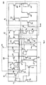
- the circuit for generating a current reference essentially comprises a pair of units G1, G2 (having identical circuit diagrams but destined to generate different references which are both substantially independent from fluctuations in the fabrication process and from fluctuations in the power supply voltage) and a circuit CL arranged to effect a linear combination of the outputs of the two units G1, G2 to achieve independence from temperature, as will be described farther on.
- each of the two units comprises: a pair of detectors S1, S2 (the term “detectors” shall hereafter be used to indicate the elements that determine the working point of the circuit, represented by the intersection point of the respective current-voltage characteristics) connected to a current mirror SP destined to inject a same current into the two detectors S1, S2; a differential amplifier AD, which constitutes the feedback circuit and is destined to generate a current signal to be provided to the mirror SP to maintain the units in the equilibrium point as the operating conditions (in particular, power supply voltage) vary; and a start-up circuit SU that injects into the detector S2, as long as the voltage across the detector itself is lower than a certain minimum value, such a current as to prevent the circuit from moving to the second equilibrium point represented by a nil value of current and voltage.
- the detector S1 is constituted by a single transistor T1 (in particular of the N type), as in the prior art, whereas the second detector S2 is constituted by a pair of transistors T2, T3, of the same type as T1, mutually connected in series. It is essential for the transconductance (or gain) characteristics of transistor T1 to be very different from those of the transistors T2, T3, so that an equilibrium point of the circuit differing from the point (0,0) of the current-voltage characteristics exists and is actually attainable. In particular, the transistor T1 has very low transconductance, whereas transistors T2, T3 have very high transconductance.
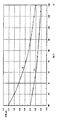
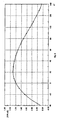
- FIG. 3 4 A possible qualitative behaviour of the characteristics of the two detectors is shown in Figures 3, 4, where C1, C2 are the characteristics of detectors S1 and S2, respectively. Due to the series arrangement of the transistors, it is evident that the pair of transistors T2, T3 has a threshold that is substantially double that of the transistor T1 and, given the different slope of the characteristics, an equilibrium point actually does exist and is represented by the intersection point of the curves C1, C2. As is well known to the person skilled in the art, in the manufacture as an integrated circuit, different characteristics can be obtained by means of a different width/length ratio of the transistors. Preferably, the width/length ratio of the transistor T1 is the reciprocal of that of the transistors T2, T3, and the gain of the transistor T1 is the inverse of that of T2 and T3.
- the reference I1 indicates the current corresponding to the equilibrium point.
- the transistor T1 and the pair of transistors T2, T3 are made very close together in the integrated circuit. Being the transistors of the same type, this guarantees a good independence from the characteristics of the technological process, for it is intuitively obvious that any fluctuation in the results of the technological process will influence the two detectors to the same extent.
- Analysis of the performance of circuits realised at different times has demonstrated that the effect of the fluctuations is in practice a parallel shift of the characteristics of the detectors, such as to leave substantially unchanged the current I1 relating to the equilibrium point, as it can be appreciated from a comparison between the Figures 3, 4, which respectively refer to a process that gives rise to a "slow” circuit and to a process that gives rise to a "fast” circuit.
- an advance in the technological manufacturing processes will have a similar influence on the two detectors.
- the differential amplifier AD is constituted by the set of transistors from T4 to T14 (where the transistors T4 to T8, T13, T14 are of the N type and the others of the P type), as is clear to the person skilled in the art.
- the transistors in AD are chosen so as to provide such a gain as to stabilise the working point with high precision, e.g. in the order of one millivolt.
- the voltage present across the two detectors S1 and S2 is applied to the gate of the transistors T4, T5.
- the current signal representative of the difference is taken at the node N1, to which the drain electrodes of the transistors T12 and T13 are connected, and is provided to the current mirror SP constituted by the transistors T15, T16, T17, of the P type.
- the transistor T14 also included in AD, only serves for stabilisation purposes.
- the transistor T20 constitutes the start-up circuit SU, whereas the transistors T19, T18 are biasing transistors of the circuit SU and of the differential amplifier AD.
- a generator like G1 guarantees a good insensitivity to the variations of the process of manufacturing the integrated circuit and of the power supply, as stated above, but it is not arranged to assure good independence from temperature.
- the transistor T1 will generally work in conditions of high saturation whereas the two transistors T2, T3, connected in series, work in a weak inversion zone. Consequently, the behaviour of the two detectors as temperature varies is different.
- the current-voltage characteristic of the detector S1 tends to become less steep as temperature grows, thus tending to lower the intersection point and hence the reference current, whereas the characteristic of the detector S2 presents a leftward shift that accentuates the lowering of the working point.
- the linear combination of the current references generated by both units G1, G2 (Fig. 1) is the characteristic of the invention that allows to achieve independence from temperature.
- the second unit G2 (which is made according to the same circuit diagram as G1 and hence has not been shown in detail), must employ detectors whose transistors have different values of the respective gains from those of the homologous transistors of G1 and such that the current I2 is different from I1 both in terms of value and in terms of behaviour as temperature varies.
- the transistors T1, T2 (or T3) of the generator G1 had a gain ratio of 1:400, whereas the corresponding transistors of the generator G2 had a gain ratio of 1:100; moreover, the decrease in 12 as temperature increases was greater than that of I1, as shown in Fig. 7.
- the linear combination circuit CL is constituted by the transistors T21 ... T25.
- the transistors T21, T22 constitute, respectively with the transistor T1 and the homologous transistor in G2, two current mirrors that supply the currents K1 ⁇ I1, K2 ⁇ I2.
- the transistors T23, T24, of the P type, constitute an additional current mirror with unit multiplication ratio which therefore supplies the current K2 ⁇ 12 anew.
- the drain electrodes of T21 and T24 are connected together and constitute a subtraction node N2 of the linear combination circuit.
- the transistor T25 which has its gate and drain electrodes connected to the node N2, constitutes the first stage of current mirrors that replicate the current generated by the circuit described in order to supply it to individual user devices.
Landscapes
- Engineering & Computer Science (AREA)
- Microelectronics & Electronic Packaging (AREA)
- Physics & Mathematics (AREA)
- Nonlinear Science (AREA)
- Electromagnetism (AREA)
- General Physics & Mathematics (AREA)
- Radar, Positioning & Navigation (AREA)
- Automation & Control Theory (AREA)
- Control Of Electrical Variables (AREA)
- Amplifiers (AREA)
Claims (8)
- CMOS-Schaltung zur Erzeugung einer Stromreferenz, mit wenigstens einer ersten Einheit (G1), die dazu bestimmt ist, einen ersten Referenzstrom (I1) zu erzeugen, und die folgenden Teilschaltungen umfaßt:dadurch gekennzeichnet, daßein erstes Element (S1) und ein zweites Element (S2) mit jeweiligen Strom-Spannungs-Charakteristiken eines solchen Verlaufs, daß sie einen Schnittpunkt aufweisen, dem der erste Referenzstrom (I1) entspricht, und von denen beide Elemente aus aktiven Komponenten aufgebaut sind und das erste Element (S1) einen ersten Transistor (T1) enthält, an dessen Ausgang der erste Referenzstrom (I1) vorliegt,eine Einrichtung (SP) zum Injizieren eines gleichen Stroms in die beiden Elemente (S1, S2),eine Starterschaltung (SU), die die Einheit dazu bringt, einen Betrieb in Übereinstimmung mit dem Schnittpunkt der Strom-Spannungs-Charakteristiken der beiden Elemente (S1, S2) zu haben, undeine Rückkopplungsschaltung zum Aufrechterhalten des Arbeitspunkts der Schaltung in Übereinstimmung mit jenem Schnittpunkt bei sich ändernden Betriebsbedingungen,der erste Transistor (T1) einer mit niedriger Verstärkung ist,das zweite Element (S2) einen zweiten Transistor (T2) und einen dritten Transistor (T3) umfaßt, die in Reihe geschaltet sind, von gleichem Dotierungstyp wie der erste Transistor (T1) sind und im Vergleich zu diesem ersten Transistor (T1) eine viel höhere Verstärkung aufweisen;die Injiziereinrichtung (SP) dazu ausgebildet ist, einen solchen Strom zu injizieren, daß der erste Transistor (T1) im Zustand einer starken Sättigung arbeitet und der zweite und der dritte Transistor (T2, T3) im Zustand einer schwachen Inversion arbeiten, unddie Rückkopplungsschaltung einen Differenzverstärker (AD) umfaßt, der an seinen Eingängen die Spannung empfängt, die am ersten Element (S1) beziehungsweise am zweiten Element (S2) anliegt, und an die Injiziereinrichtung (SP) ein Steuersignal so liefert, daß die Schaltung in diesem Arbeitspunkt verbleibt.
- Schaltung nach Anspruch 1, dadurch gekennzeichnet, daß sie weiterhin eine zweite Einheit (G2) zum Erzeugen eines Referenzstroms (I2) umfaßt, die den gleichen Aufbau wie die erste Einheit (G1) hat und ein erstes und ein zweites Element mit jeweiligen solchen Strom-Spannungs-Charakteristiken enthält, daß der Schnittpunkt einem Stromwert (I2) entspricht, der sich von dem der Charakteristiken des ersten und des zweiten Elements der ersten Einheit unterscheidet, und daß die beiden Einheiten mit einer Einrichtung (CL) für die lineare Kombination der jeweiligen Ströme verbunden sind.
- Schaltung nach Anspruch 2, dadurch gekennzeichnet, daß die erste Einheit (G1) und die zweite Einheit (G2) dazu ausgebildet sind, Ströme zu erzeugen, die ein unterschiedliches Temperaturverhalten zeigen.
- Schaltung nach einem der Ansprüche 2 bis 3, dadurch gekennzeichnet, daß in beiden Einheiten (G1, G2) der erste Transistor (T1) eine Verstärkung aufweist, die invers der Verstärkung des zweiten und des dritten Transistors (T2, T3) ist.
- Schaltung nach Anspruch 4, dadurch gekennzeichnet, daß das Verhältnis zwischen den Verstärkungen des ersten Transistors (T1) und des zweiten oder des dritten Transistors (T2, T3) der ersten Einheit (G1) in der Größenordnung von 1 : 400 ist.
- Schaltung nach Anspruch 4 oder 5, dadurch gekennzeichnet, daß das Verhältnis zwischen den Verstärkungen des ersten Transistors und des zweiten oder dritten Transistors der zweiten Einheit (G2) in der Größenordnung von 1 : 100 ist.
- Schaltung nach einem der Ansprüche 2 bis 6, dadurch gekennzeichnet, daß die zweite Einheit (G2) dazu ausgebildet ist, einen Strom zu erzeugen, dessen Variation innerhalb eines gegebenen Temperaturbereichs größer ist als die Variation des Stroms der ersten Einheit (G1) im selben Bereich.
- Schaltung nach einem der Ansprüche 2 bis 7, dadurch gekennzeichnet, daß die Einrichtung (CL) zu linearen Kombination die folgendermaßen geschalteten Transistoren umfaßt:einen vierten Transistor (T21) und einen fünften Transistor (T22), die mit dem ersten Transistor (T1) der ersten Einheit (G1) beziehungsweise mit dem ersten Transistor (T1) der zweiten Einheit (G2) so verbunden sind, daß sie mit diesen einen ersten und einen zweiten Stromspiegel bilden, die die von der ersten beziehungsweise von der zweiten Einheit gelieferten Ströme (I1, I2) mit jeweiligen Faktoren multiplizieren,einen sechsten Transistor (T23) und einen siebten Transistor (T24), die einen dritten Stromspiegel (T23, T24) bilden, der dazu geschaltet ist, das Vorzeichen des aus dem zweiten Spiegel kommenden Stroms zu invertieren, wobei der siebte Transistor (T24) und der vierte Transistor (T21) eine gemeinsame Elektrode haben, die einen Subtraktionsknotenpunkt (N2) für die vom ersten und vom dritten Spiegel gelieferten Ströme bildet,einen achten Transistor (T25), dessen Steuerelektrode und dessen Abflußelektrode mit dem Subtraktionsknotenpunkt (N2) verbunden sind und der die erste Stufe eines zusätzlichen Stromspiegels bildet, der dazu bestimmt ist, den von der Schaltung erzeugten Referenzstrom an Anwendungsvorrichtungen abzugeben.
Applications Claiming Priority (2)
| Application Number | Priority Date | Filing Date | Title |
|---|---|---|---|
| ITTO980831 | 1998-10-05 | ||
| IT1998TO000831A IT1304670B1 (it) | 1998-10-05 | 1998-10-05 | Circuito in tecnologia cmos per la generazione di un riferimento incorrente. |
Publications (3)
| Publication Number | Publication Date |
|---|---|
| EP0992871A2 EP0992871A2 (de) | 2000-04-12 |
| EP0992871A3 EP0992871A3 (de) | 2000-04-26 |
| EP0992871B1 true EP0992871B1 (de) | 2004-01-07 |
Family
ID=11417077
Family Applications (1)
| Application Number | Title | Priority Date | Filing Date |
|---|---|---|---|
| EP99119497A Expired - Lifetime EP0992871B1 (de) | 1998-10-05 | 1999-10-01 | CMOS-Schaltung zur Erzeugung einer Stromreferenz |
Country Status (6)
| Country | Link |
|---|---|
| US (1) | US6166587A (de) |
| EP (1) | EP0992871B1 (de) |
| JP (1) | JP3181898B2 (de) |
| CA (1) | CA2284956C (de) |
| DE (1) | DE69914037T2 (de) |
| IT (1) | IT1304670B1 (de) |
Families Citing this family (5)
| Publication number | Priority date | Publication date | Assignee | Title |
|---|---|---|---|---|
| US6346848B1 (en) * | 2000-06-29 | 2002-02-12 | International Business Machines Corporation | Apparatus and method for generating current linearly dependent on temperature |
| US6466081B1 (en) * | 2000-11-08 | 2002-10-15 | Applied Micro Circuits Corporation | Temperature stable CMOS device |
| US6304109B1 (en) * | 2000-12-05 | 2001-10-16 | Analog Devices, Inc. | High gain CMOS amplifier |
| GB0211564D0 (en) * | 2002-05-21 | 2002-06-26 | Tournaz Technology Ltd | Reference circuit |
| KR100668414B1 (ko) | 2004-12-10 | 2007-01-16 | 한국전자통신연구원 | 기준 전류 발생기 |
Family Cites Families (7)
| Publication number | Priority date | Publication date | Assignee | Title |
|---|---|---|---|---|
| FR2494519A1 (fr) * | 1980-11-14 | 1982-05-21 | Efcis | Generateur de courant integre en technologie cmos |
| US4645948A (en) * | 1984-10-01 | 1987-02-24 | At&T Bell Laboratories | Field effect transistor current source |
| US4684898A (en) * | 1985-05-15 | 1987-08-04 | Signetics Corporation | Temperature and process variation compensation for a delta demodulation decoder |
| US5157285A (en) * | 1991-08-30 | 1992-10-20 | Allen Michael J | Low noise, temperature-compensated, and process-compensated current and voltage control circuits |
| US5331295A (en) * | 1993-02-03 | 1994-07-19 | National Semiconductor Corporation | Voltage controlled oscillator with efficient process compensation |
| JP3157746B2 (ja) * | 1997-06-30 | 2001-04-16 | 日本電気アイシーマイコンシステム株式会社 | 定電流回路 |
| US5939933A (en) * | 1998-02-13 | 1999-08-17 | Adaptec, Inc. | Intentionally mismatched mirror process inverse current source |
-
1998
- 1998-10-05 IT IT1998TO000831A patent/IT1304670B1/it active
-
1999
- 1999-09-29 US US09/409,033 patent/US6166587A/en not_active Expired - Lifetime
- 1999-10-01 DE DE69914037T patent/DE69914037T2/de not_active Expired - Lifetime
- 1999-10-01 EP EP99119497A patent/EP0992871B1/de not_active Expired - Lifetime
- 1999-10-04 CA CA002284956A patent/CA2284956C/en not_active Expired - Fee Related
- 1999-10-04 JP JP28288799A patent/JP3181898B2/ja not_active Expired - Fee Related
Also Published As
| Publication number | Publication date |
|---|---|
| CA2284956A1 (en) | 2000-04-05 |
| EP0992871A3 (de) | 2000-04-26 |
| IT1304670B1 (it) | 2001-03-28 |
| JP2000122740A (ja) | 2000-04-28 |
| US6166587A (en) | 2000-12-26 |
| ITTO980831A1 (it) | 2000-04-05 |
| DE69914037T2 (de) | 2004-07-08 |
| DE69914037D1 (de) | 2004-02-12 |
| EP0992871A2 (de) | 2000-04-12 |
| JP3181898B2 (ja) | 2001-07-03 |
| CA2284956C (en) | 2003-08-12 |
Similar Documents
| Publication | Publication Date | Title |
|---|---|---|
| US4287439A (en) | MOS Bandgap reference | |
| US4264874A (en) | Low voltage CMOS amplifier | |
| KR0153545B1 (ko) | 기준 전위 발생 회로 | |
| US10061340B1 (en) | Bandgap reference voltage generator | |
| US4730168A (en) | CMOS output stage with large voltage swing and with stabilization of the quiescent current | |
| US5448158A (en) | PTAT current source | |
| US5568045A (en) | Reference voltage generator of a band-gap regulator type used in CMOS transistor circuit | |
| US5793254A (en) | Monolithic amplifier with stable, high resistance feedback element and method for fabricating the same | |
| US5612614A (en) | Current mirror and self-starting reference current generator | |
| US5614816A (en) | Low voltage reference circuit and method of operation | |
| KR100235809B1 (ko) | 차동증폭 및 출력오프셋회로와 이를 구비한 반도체집적회로 및 노이즈 제거방법 | |
| JP2000112550A (ja) | 超低電圧カスコ―ドカレントミラ― | |
| JPH07104877A (ja) | 禁止帯幅基準電圧源 | |
| US4524318A (en) | Band gap voltage reference circuit | |
| US5483196A (en) | Amplifier architecture and application thereof to a band-gap voltage generator | |
| US5436594A (en) | Fully differential transconductance amplifier with common-mode output voltage stabilization | |
| US4999521A (en) | CMOS analog multiplying circuit | |
| JPS5925243B2 (ja) | 定電流源 | |
| US6166587A (en) | CMOS circuit for generating a current reference, the circuit comprising a transistor in a weak inversion region | |
| JPH0583003B2 (de) | ||
| US5469111A (en) | Circuit for generating a process variation insensitive reference bias current | |
| US6014020A (en) | Reference voltage source with compensated temperature dependency and method for operating the same | |
| US5278518A (en) | Amplifying circuit with exponential gain control | |
| JP3354538B2 (ja) | Cmos集積回路におけるプロセス及び動作パラメータの変動を補償するための装置 | |
| US3480872A (en) | Direct-coupled differential input amplifier |
Legal Events
| Date | Code | Title | Description |
|---|---|---|---|
| PUAI | Public reference made under article 153(3) epc to a published international application that has entered the european phase |
Free format text: ORIGINAL CODE: 0009012 |
|
| PUAL | Search report despatched |
Free format text: ORIGINAL CODE: 0009013 |
|
| AK | Designated contracting states |
Kind code of ref document: A2 Designated state(s): DE FR GB IT NL SE |
|
| AX | Request for extension of the european patent |
Free format text: AL;LT;LV;MK;RO;SI |
|
| AK | Designated contracting states |
Kind code of ref document: A3 Designated state(s): AT BE CH CY DE DK ES FI FR GB GR IE IT LI LU MC NL PT SE |
|
| AX | Request for extension of the european patent |
Free format text: AL;LT;LV;MK;RO;SI |
|
| RIC1 | Information provided on ipc code assigned before grant |
Free format text: 7H 03L 7/089 A, 7G 05F 3/26 B |
|
| 17P | Request for examination filed |
Effective date: 20000509 |
|
| AKX | Designation fees paid |
Free format text: DE FR GB IT NL SE |
|
| RAP1 | Party data changed (applicant data changed or rights of an application transferred) |
Owner name: TELECOM ITALIA LAB S.P.A. |
|
| GRAH | Despatch of communication of intention to grant a patent |
Free format text: ORIGINAL CODE: EPIDOS IGRA |
|
| RAP1 | Party data changed (applicant data changed or rights of an application transferred) |
Owner name: TELECOM ITALIA S.P.A. |
|
| GRAS | Grant fee paid |
Free format text: ORIGINAL CODE: EPIDOSNIGR3 |
|
| GRAA | (expected) grant |
Free format text: ORIGINAL CODE: 0009210 |
|
| AK | Designated contracting states |
Kind code of ref document: B1 Designated state(s): DE FR GB IT NL SE |
|
| REG | Reference to a national code |
Ref country code: GB Ref legal event code: FG4D |
|
| REF | Corresponds to: |
Ref document number: 69914037 Country of ref document: DE Date of ref document: 20040212 Kind code of ref document: P |
|
| REG | Reference to a national code |
Ref country code: SE Ref legal event code: TRGR |
|
| ET | Fr: translation filed | ||
| PLBE | No opposition filed within time limit |
Free format text: ORIGINAL CODE: 0009261 |
|
| STAA | Information on the status of an ep patent application or granted ep patent |
Free format text: STATUS: NO OPPOSITION FILED WITHIN TIME LIMIT |
|
| 26N | No opposition filed |
Effective date: 20041008 |
|
| REG | Reference to a national code |
Ref country code: FR Ref legal event code: PLFP Year of fee payment: 17 |
|
| PGFP | Annual fee paid to national office [announced via postgrant information from national office to epo] |
Ref country code: IT Payment date: 20151026 Year of fee payment: 17 Ref country code: DE Payment date: 20151028 Year of fee payment: 17 Ref country code: GB Payment date: 20151027 Year of fee payment: 17 |
|
| PGFP | Annual fee paid to national office [announced via postgrant information from national office to epo] |
Ref country code: FR Payment date: 20151019 Year of fee payment: 17 Ref country code: SE Payment date: 20151028 Year of fee payment: 17 Ref country code: NL Payment date: 20151026 Year of fee payment: 17 |
|
| REG | Reference to a national code |
Ref country code: DE Ref legal event code: R119 Ref document number: 69914037 Country of ref document: DE |
|
| REG | Reference to a national code |
Ref country code: NL Ref legal event code: MM Effective date: 20161101 |
|
| GBPC | Gb: european patent ceased through non-payment of renewal fee |
Effective date: 20161001 |
|
| REG | Reference to a national code |
Ref country code: FR Ref legal event code: ST Effective date: 20170630 |
|
| PG25 | Lapsed in a contracting state [announced via postgrant information from national office to epo] |
Ref country code: GB Free format text: LAPSE BECAUSE OF NON-PAYMENT OF DUE FEES Effective date: 20161001 Ref country code: FR Free format text: LAPSE BECAUSE OF NON-PAYMENT OF DUE FEES Effective date: 20161102 Ref country code: DE Free format text: LAPSE BECAUSE OF NON-PAYMENT OF DUE FEES Effective date: 20170503 |
|
| PG25 | Lapsed in a contracting state [announced via postgrant information from national office to epo] |
Ref country code: NL Free format text: LAPSE BECAUSE OF NON-PAYMENT OF DUE FEES Effective date: 20161101 Ref country code: SE Free format text: LAPSE BECAUSE OF NON-PAYMENT OF DUE FEES Effective date: 20161002 |
|
| PG25 | Lapsed in a contracting state [announced via postgrant information from national office to epo] |
Ref country code: IT Free format text: LAPSE BECAUSE OF NON-PAYMENT OF DUE FEES Effective date: 20161001 |