EP0992914A2 - Dispositif de transfert de données entre des noeuds d'ordinateur - Google Patents
Dispositif de transfert de données entre des noeuds d'ordinateur Download PDFInfo
- Publication number
- EP0992914A2 EP0992914A2 EP99119683A EP99119683A EP0992914A2 EP 0992914 A2 EP0992914 A2 EP 0992914A2 EP 99119683 A EP99119683 A EP 99119683A EP 99119683 A EP99119683 A EP 99119683A EP 0992914 A2 EP0992914 A2 EP 0992914A2
- Authority
- EP
- European Patent Office
- Prior art keywords
- circuit
- receiving
- data
- bus
- node
- Prior art date
- Legal status (The legal status is an assumption and is not a legal conclusion. Google has not performed a legal analysis and makes no representation as to the accuracy of the status listed.)
- Granted
Links
Images

Classifications
-
- G—PHYSICS
- G06—COMPUTING OR CALCULATING; COUNTING
- G06F—ELECTRIC DIGITAL DATA PROCESSING
- G06F13/00—Interconnection of, or transfer of information or other signals between, memories, input/output devices or central processing units
- G06F13/38—Information transfer, e.g. on bus
- G06F13/42—Bus transfer protocol, e.g. handshake; Synchronisation
- G06F13/4265—Bus transfer protocol, e.g. handshake; Synchronisation on a point to point bus
-
- Y—GENERAL TAGGING OF NEW TECHNOLOGICAL DEVELOPMENTS; GENERAL TAGGING OF CROSS-SECTIONAL TECHNOLOGIES SPANNING OVER SEVERAL SECTIONS OF THE IPC; TECHNICAL SUBJECTS COVERED BY FORMER USPC CROSS-REFERENCE ART COLLECTIONS [XRACs] AND DIGESTS
- Y02—TECHNOLOGIES OR APPLICATIONS FOR MITIGATION OR ADAPTATION AGAINST CLIMATE CHANGE
- Y02D—CLIMATE CHANGE MITIGATION TECHNOLOGIES IN INFORMATION AND COMMUNICATION TECHNOLOGIES [ICT], I.E. INFORMATION AND COMMUNICATION TECHNOLOGIES AIMING AT THE REDUCTION OF THEIR OWN ENERGY USE
- Y02D10/00—Energy efficient computing, e.g. low power processors, power management or thermal management
Definitions
- the present invention relates to a data transferring device for communicating data between a plurality of nodes. More specifically, the present invention relates to a data transferring device capable of selectively using one of multiple data transfer rates between nodes.
- the IEEE 1394-1995 standard As an international standard for high-speed serial bus transfer methods, the IEEE 1394-1995 standard has been known in the art. In this IEEE 1394-1995 standard, although it is possible to couple a plurality of nodes of different data transfer capabilities to a single bus, the maximum data transfer capability between two nodes depends on the maximum data transfer capability of a node existing between these two nodes. More specifically, three different data transfer rates of 100, 200, and 400 megabits per second (Mbps) are supported, and it is possible to learn the data transfer rate of a connection destination by the process of bus initialization or by the application of a speed signal just before a packet transfer.
- Mbps megabits per second
- an object of the present invention is to provide a data transferring device capable of configuring an optimal circuit according to the data transfer capability of a connection destination for achieving the reduction of power consumption.
- the present invention discloses a first data transferring device which is constructed of at least two nodes of which first and second nodes are coupled together by a bus, wherein the first node includes a detecting circuit for detecting the maximum data transfer capability of a connected node, at least two receiving circuits for receiving data from the bus, and a controlling circuit for selecting, based on an output signal from the detecting circuit, one of the receiving circuits and for performing control so as to bring the other of the receiving circuits to a stop, and wherein the second node includes a transmitting circuit for transmitting data to the bus and a notifying circuit for notifying the first node of its own maximum data transfer capability via the transmitting circuit.
- the present invention discloses a second data transferring device which is constructed of at least two nodes of which first and second nodes are coupled together by a bus, wherein the first node includes a detecting circuit for detecting the maximum data transfer capability of a connected node, a receiving circuit for receiving data from the bus, a bias adjusting circuit for adjusting a bias for the receiving circuit, and a controlling circuit for controlling, based on an output signal from the detecting circuit, the bias adjusting circuit, and wherein the second node includes a transmitting circuit for transmitting data to the bus and a notifying circuit for notifying the first node of its own maximum data transfer capability via the transmitting circuit.
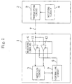
- the present data transferring device is constructed of at least two nodes (the number of nodes is two in the present embodiment). Connected between first and second nodes 1 and 2 is a bus 7 .
- the first node 1 includes a receiving unit 4 having at least two receiving circuits for receiving data from the bus 7 , a detecting circuit 3 for detecting the maximum data transfer capability of a node as a connection destination, and a controlling circuit 5 for selecting, based on an output signal from the detecting circuit 3 , one of the two receiving circuits and for controlling the receiving unit 4 so as to bring the other receiving circuit to a stop.
- Outputs of the receiving unit 4 are coupled to the detecting circuit 3 .
- An output signal from the detecting circuit 3 is coupled to the controlling circuit 5 .
- an output of the controlling circuit 5 is coupled to the receiving unit 4 by a controlling signal 6 .
- the receiving unit 4 is constructed of a receiving circuit 41 for high-speed data transfers (hereinafter called the high-speed receiving circuit) and a receiving circuit 42 for low-speed data transfers (hereinafter called the low-speed receiving circuit).
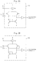
- Figures 2A and 2B are circuit diagrams showing details of these two receiving circuits 41 and 42 .
- the receiving circuits 41 and 42 each are implemented by a differential input amplifier having PMOS transistors as an input gate, wherein the value of a bias current lb1 which is applied to the high-speed receiving circuit 41 is set lower than that of a bias current lb2 which is applied to the low-speed receiving circuit 42.
- the second node 2 includes a transmitting circuit 9 for transmitting data to the bus 7 and a notifying circuit 8 for notifying, via the transmitting circuit 9 , the first node 1 of its own maximum data transfer capability.
- the detection circuit 3 is able to learn the data transfer capability of a connection destination according to a signal from the notifying circuit 8 .
- the detecting circuit 3 sends to the controlling circuit 5 such acquired knowledge in the form of a signal.
- the controlling signal 5 selects between the high-speed receiving circuit 41 and the low-speed receiving circuit 42 as follows. If the received signal indicates that the data transfer capability of a connection destination is high, the high-speed receiving circuit 41 is then selected, while the low-speed receiving circuit 42 is brought to a stop by the controlling signal 6 . On the other hand, if the received signal indicates that the data transfer capability of a connection destination is low, the low-speed receiving circuit 42 is then selected, while the high-speed receiving circuit 41 is brought to a stop by the controlling signal 6 .
- selection between the high-speed receiving circuit 41 and the low-speed receiving circuit 42 is made depending on the connection destination's data transfer capability, therefore making it possible to architect an optimal circuit configuration.
- bias current will become less than when the high-speed receiving circuit 41 is selected. This provides the effect of reducing unnecessary power consumption when the data transfer capability of a connection destination is lower than that of the first node 1 itself.
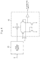
- the receiving unit 4 is constructed of a receiving circuit 44 which serves not only as a high-speed receiving circuit but also as a low-speed receiving circuit and a bias adjusting circuit 43 for adjusting a bias current for the receiving circuit 44, and an output signal of the bias adjusting circuit 43 is fed to the receiving circuit 44.
- Figure 4 shows in detail the structure of the receiving circuit 44.
- the bias adjusting circuit 43 adjusts a bias current for the receiving circuit 44. In other words, if the data transfer capability of a connection destination is high, it is set such that a bias current lb3 will flow in greater quantity. On the other hand, if the data transfer capability of a connection destination is low, it is set such that the bias current lb3 will flow in less quantity.
- the controlling circuit 5 controls, based on an output signal from the detecting circuit 3 , the bias adjusting circuit 43, whereby the bias current lb3 can be set to an appropriate value according to the connection destination's data transfer capability.
- the bias current lb3 can be set to an appropriate value according to the connection destination's data transfer capability.
Landscapes
- Engineering & Computer Science (AREA)
- Theoretical Computer Science (AREA)
- Physics & Mathematics (AREA)
- General Engineering & Computer Science (AREA)
- General Physics & Mathematics (AREA)
- Dc Digital Transmission (AREA)
- Communication Control (AREA)
- Small-Scale Networks (AREA)
- Logic Circuits (AREA)
- Information Transfer Systems (AREA)
Priority Applications (1)
| Application Number | Priority Date | Filing Date | Title |
|---|---|---|---|
| EP03014943A EP1355236B1 (fr) | 1998-10-07 | 1999-10-05 | Dispositif de transfert de donnees |
Applications Claiming Priority (2)
| Application Number | Priority Date | Filing Date | Title |
|---|---|---|---|
| JP10284907A JP2000112877A (ja) | 1998-10-07 | 1998-10-07 | データ転送装置 |
| JP28490798 | 1998-10-07 |
Related Child Applications (1)
| Application Number | Title | Priority Date | Filing Date |
|---|---|---|---|
| EP03014943A Division EP1355236B1 (fr) | 1998-10-07 | 1999-10-05 | Dispositif de transfert de donnees |
Publications (3)
| Publication Number | Publication Date |
|---|---|
| EP0992914A2 true EP0992914A2 (fr) | 2000-04-12 |
| EP0992914A3 EP0992914A3 (fr) | 2002-07-17 |
| EP0992914B1 EP0992914B1 (fr) | 2004-01-07 |
Family
ID=17684601
Family Applications (2)
| Application Number | Title | Priority Date | Filing Date |
|---|---|---|---|
| EP99119683A Expired - Lifetime EP0992914B1 (fr) | 1998-10-07 | 1999-10-05 | Dispositif de transfert de données entre des noeuds d'ordinateur |
| EP03014943A Expired - Lifetime EP1355236B1 (fr) | 1998-10-07 | 1999-10-05 | Dispositif de transfert de donnees |
Family Applications After (1)
| Application Number | Title | Priority Date | Filing Date |
|---|---|---|---|
| EP03014943A Expired - Lifetime EP1355236B1 (fr) | 1998-10-07 | 1999-10-05 | Dispositif de transfert de donnees |
Country Status (4)
| Country | Link |
|---|---|
| US (1) | US6633588B1 (fr) |
| EP (2) | EP0992914B1 (fr) |
| JP (1) | JP2000112877A (fr) |
| DE (2) | DE69914038T2 (fr) |
Families Citing this family (1)
| Publication number | Priority date | Publication date | Assignee | Title |
|---|---|---|---|---|
| JP4512599B2 (ja) * | 2005-09-26 | 2010-07-28 | パナソニック株式会社 | 単線双方向通信装置及びシステム |
Family Cites Families (21)
| Publication number | Priority date | Publication date | Assignee | Title |
|---|---|---|---|---|
| US3747074A (en) | 1972-03-17 | 1973-07-17 | Comteu | Method of and apparatus for baud rate detection |
| US5579486A (en) * | 1993-01-14 | 1996-11-26 | Apple Computer, Inc. | Communication node with a first bus configuration for arbitration and a second bus configuration for data transfer |
| US5509126A (en) * | 1993-03-16 | 1996-04-16 | Apple Computer, Inc. | Method and apparatus for a dynamic, multi-speed bus architecture having a scalable interface |
| US5559967A (en) | 1993-03-18 | 1996-09-24 | Apple Computer, Inc. | Method and apparatus for a dynamic, multi-speed bus architecture in which an exchange of speed messages occurs independent of the data signal transfers |
| US5384769A (en) * | 1993-03-19 | 1995-01-24 | Apple Computer, Inc. | Method and apparatus for a bus transceiver incorporating a high speed binary data transfer mode with a ternary control transfer mode having a full duplex, dominant logic transmission scheme |
| US5325355A (en) * | 1993-03-19 | 1994-06-28 | Apple Computer, Inc. | Method and apparatus for implementing a common mode level shift in a bus transceiver incorporating a high speed binary data transfer mode with a ternary control transfer mode |
| US5424657A (en) * | 1993-03-19 | 1995-06-13 | Apple Computer, Inc. | Method and apparatus for implementing a common mode level shift in a bus transceiver incorporating a high speed binary data transfer mode with a ternary control transfer mode |
| US5493657A (en) * | 1993-06-21 | 1996-02-20 | Apple Computer, Inc. | High speed dominant mode bus for differential signals |
| US5592510A (en) * | 1994-03-29 | 1997-01-07 | Apple Computer, Inc. | Common mode early voltage compensation subcircuit for current driver |
| US5485488A (en) | 1994-03-29 | 1996-01-16 | Apple Computer, Inc. | Circuit and method for twisted pair current source driver |
| US5504757A (en) * | 1994-09-27 | 1996-04-02 | International Business Machines Corporation | Method for selecting transmission speeds for transmitting data packets over a serial bus |
| US5828733A (en) | 1995-04-03 | 1998-10-27 | Advanced Micro Devices, Inc. | Method and arrangement for increasing data transmisssion rate over telephone cable |
| US5802057A (en) | 1995-12-01 | 1998-09-01 | Apple Computer, Inc. | Fly-by serial bus arbitration |
| JPH1023024A (ja) | 1996-07-03 | 1998-01-23 | Sony Corp | Atm交換装置およびその方法 |
| JPH1065758A (ja) | 1996-08-23 | 1998-03-06 | Sony Corp | データ伝送方法及び装置 |
| JPH1065718A (ja) * | 1996-08-23 | 1998-03-06 | Sony Corp | データ伝送方法及び装置 |
| US5913075A (en) * | 1997-03-25 | 1999-06-15 | International Business Machines Corporation | High speed communication between high cycle rate electronic devices using a low cycle rate bus |
| US5907553A (en) * | 1997-04-08 | 1999-05-25 | Level One Communications, Inc. | Power savings in multiple technology physical layer devices supporting autonegotiation |
| US5978869A (en) * | 1997-07-21 | 1999-11-02 | International Business Machines Corporation | Enhanced dual speed bus computer system |
| US5958033A (en) * | 1997-08-13 | 1999-09-28 | Hewlett Packard Company | On- the-fly partitionable computer bus for enhanced operation with varying bus clock frequencies |
| US6425041B1 (en) * | 1998-06-05 | 2002-07-23 | Micron Technology, Inc. | Time-multiplexed multi-speed bus |
-
1998
- 1998-10-07 JP JP10284907A patent/JP2000112877A/ja active Pending
-
1999
- 1999-10-01 US US09/410,764 patent/US6633588B1/en not_active Expired - Lifetime
- 1999-10-05 DE DE69914038T patent/DE69914038T2/de not_active Expired - Lifetime
- 1999-10-05 EP EP99119683A patent/EP0992914B1/fr not_active Expired - Lifetime
- 1999-10-05 DE DE69933060T patent/DE69933060T2/de not_active Expired - Lifetime
- 1999-10-05 EP EP03014943A patent/EP1355236B1/fr not_active Expired - Lifetime
Also Published As
| Publication number | Publication date |
|---|---|
| EP0992914A3 (fr) | 2002-07-17 |
| JP2000112877A (ja) | 2000-04-21 |
| DE69933060T2 (de) | 2006-12-21 |
| EP1355236A3 (fr) | 2005-08-10 |
| DE69914038T2 (de) | 2004-06-09 |
| US6633588B1 (en) | 2003-10-14 |
| EP0992914B1 (fr) | 2004-01-07 |
| DE69933060D1 (de) | 2006-10-12 |
| DE69914038D1 (de) | 2004-02-12 |
| EP1355236B1 (fr) | 2006-08-30 |
| EP1355236A2 (fr) | 2003-10-22 |
Similar Documents
| Publication | Publication Date | Title |
|---|---|---|
| EP1443723B1 (fr) | Procédé de communication pour une interface indépendante du media (MII) pour un élément à haute integration d'un réseau ethernet | |
| US5493657A (en) | High speed dominant mode bus for differential signals | |
| JP3943574B2 (ja) | 2進データ送信モードおよび3進制御送信モードを有するバス・トランシーバ | |
| US20040130347A1 (en) | Hypertransport/SPI-4 interface supporting configurable deskewing | |
| US8443125B2 (en) | Single pin read-write method and interface | |
| US7724689B2 (en) | Interface device and interface device control method | |
| US6567909B2 (en) | Parallel processor system | |
| US20040104829A1 (en) | Parallel to serial conversion device and method | |
| US5903508A (en) | Input buffer of memory device for reducing current consumption in standby mode | |
| EP1355236B1 (fr) | Dispositif de transfert de donnees | |
| CN100362751C (zh) | 具有模式转换电路的双模式移动终端 | |
| EP1361777B1 (fr) | Un protocole synchrone de communication pour des dispositives asynchrones | |
| US7924826B1 (en) | Method and apparatus for device pinout mapping | |
| US7529202B2 (en) | Communication data processing circuit | |
| WO1997009811A1 (fr) | Circuit de commande de sortie a sortie unique, a faible instabilite et faible consommation | |
| JPH09162916A (ja) | スイッチングハブ | |
| JP3995131B2 (ja) | データ出力回路 | |
| JP5902402B2 (ja) | データ出力調整装置、データ出力調整方法、rgmiiネットワークシステム、及び、rgmiiネットワーク通信路切替方法 | |
| JP2000286855A (ja) | 通信システム及び通信機器 | |
| US6297675B1 (en) | Semiconductor integrated circuit and semiconductor integrated circuit system having serially interconnectable data buses | |
| US6628656B1 (en) | Circuit, method and/or architecture for improving the performance of a serial communication link | |
| JP3334007B2 (ja) | 切換え式伝送装置 | |
| JP2924029B2 (ja) | 情報転送方式 | |
| JPH0870295A (ja) | 信号伝送方法 | |
| JPH09247069A (ja) | 衛星通信システム |
Legal Events
| Date | Code | Title | Description |
|---|---|---|---|
| PUAI | Public reference made under article 153(3) epc to a published international application that has entered the european phase |
Free format text: ORIGINAL CODE: 0009012 |
|
| AK | Designated contracting states |
Kind code of ref document: A2 Designated state(s): AT BE CH CY DE DK ES FI FR GB GR IE IT LI LU MC NL PT SE |
|
| AX | Request for extension of the european patent |
Free format text: AL;LT;LV;MK;RO;SI |
|
| RAP1 | Party data changed (applicant data changed or rights of an application transferred) |
Owner name: MATSUSHITA ELECTRIC INDUSTRIAL CO., LTD. |
|
| PUAL | Search report despatched |
Free format text: ORIGINAL CODE: 0009013 |
|
| AK | Designated contracting states |
Kind code of ref document: A3 Designated state(s): AT BE CH CY DE DK ES FI FR GB GR IE IT LI LU MC NL PT SE |
|
| AX | Request for extension of the european patent |
Free format text: AL;LT;LV;MK;RO;SI |
|
| 17P | Request for examination filed |
Effective date: 20021004 |
|
| 17Q | First examination report despatched |
Effective date: 20021128 |
|
| AKX | Designation fees paid |
Designated state(s): DE FR GB |
|
| GRAH | Despatch of communication of intention to grant a patent |
Free format text: ORIGINAL CODE: EPIDOS IGRA |
|
| GRAS | Grant fee paid |
Free format text: ORIGINAL CODE: EPIDOSNIGR3 |
|
| GRAA | (expected) grant |
Free format text: ORIGINAL CODE: 0009210 |
|
| AK | Designated contracting states |
Kind code of ref document: B1 Designated state(s): DE FR GB |
|
| REG | Reference to a national code |
Ref country code: GB Ref legal event code: FG4D |
|
| REG | Reference to a national code |
Ref country code: IE Ref legal event code: FG4D |
|
| REF | Corresponds to: |
Ref document number: 69914038 Country of ref document: DE Date of ref document: 20040212 Kind code of ref document: P |
|
| ET | Fr: translation filed | ||
| PLBE | No opposition filed within time limit |
Free format text: ORIGINAL CODE: 0009261 |
|
| STAA | Information on the status of an ep patent application or granted ep patent |
Free format text: STATUS: NO OPPOSITION FILED WITHIN TIME LIMIT |
|
| 26N | No opposition filed |
Effective date: 20041008 |
|
| REG | Reference to a national code |
Ref country code: IE Ref legal event code: MM4A |
|
| PGFP | Annual fee paid to national office [announced via postgrant information from national office to epo] |
Ref country code: GB Payment date: 20100929 Year of fee payment: 12 |
|
| PGFP | Annual fee paid to national office [announced via postgrant information from national office to epo] |
Ref country code: FR Payment date: 20101020 Year of fee payment: 12 |
|
| PGFP | Annual fee paid to national office [announced via postgrant information from national office to epo] |
Ref country code: DE Payment date: 20100929 Year of fee payment: 12 |
|
| GBPC | Gb: european patent ceased through non-payment of renewal fee |
Effective date: 20111005 |
|
| REG | Reference to a national code |
Ref country code: FR Ref legal event code: ST Effective date: 20120629 |
|
| PG25 | Lapsed in a contracting state [announced via postgrant information from national office to epo] |
Ref country code: DE Free format text: LAPSE BECAUSE OF NON-PAYMENT OF DUE FEES Effective date: 20120501 |
|
| REG | Reference to a national code |
Ref country code: DE Ref legal event code: R119 Ref document number: 69914038 Country of ref document: DE Effective date: 20120501 |
|
| PG25 | Lapsed in a contracting state [announced via postgrant information from national office to epo] |
Ref country code: FR Free format text: LAPSE BECAUSE OF NON-PAYMENT OF DUE FEES Effective date: 20111102 Ref country code: GB Free format text: LAPSE BECAUSE OF NON-PAYMENT OF DUE FEES Effective date: 20111005 |