EP0993019A2 - Verfahren zur Reduzierung von Artefakterscheinungen in der Raster-Elektronenmikroskopie - Google Patents
Verfahren zur Reduzierung von Artefakterscheinungen in der Raster-Elektronenmikroskopie Download PDFInfo
- Publication number
- EP0993019A2 EP0993019A2 EP99118816A EP99118816A EP0993019A2 EP 0993019 A2 EP0993019 A2 EP 0993019A2 EP 99118816 A EP99118816 A EP 99118816A EP 99118816 A EP99118816 A EP 99118816A EP 0993019 A2 EP0993019 A2 EP 0993019A2
- Authority
- EP
- European Patent Office
- Prior art keywords
- pixel
- sub
- scanning
- image
- scanning beam
- Prior art date
- Legal status (The legal status is an assumption and is not a legal conclusion. Google has not performed a legal analysis and makes no representation as to the accuracy of the status listed.)
- Granted
Links
Images



Classifications
-
- H—ELECTRICITY
- H01—ELECTRIC ELEMENTS
- H01J—ELECTRIC DISCHARGE TUBES OR DISCHARGE LAMPS
- H01J37/00—Discharge tubes with provision for introducing objects or material to be exposed to the discharge, e.g. for the purpose of examination or processing thereof
- H01J37/26—Electron or ion microscopes; Electron or ion diffraction tubes
- H01J37/28—Electron or ion microscopes; Electron or ion diffraction tubes with scanning beams
-
- H—ELECTRICITY
- H01—ELECTRIC ELEMENTS
- H01J—ELECTRIC DISCHARGE TUBES OR DISCHARGE LAMPS
- H01J37/00—Discharge tubes with provision for introducing objects or material to be exposed to the discharge, e.g. for the purpose of examination or processing thereof
- H01J37/02—Details
- H01J37/22—Optical, image processing or photographic arrangements associated with the tube
- H01J37/222—Image processing arrangements associated with the tube
Definitions
- the present invention relates to a method for improving the quality of images obtained from scanning beam microscopy. More particularly, the invention relates to a method for reducing aliasing effects in scanning beam microscopy.
- a particularly important relationship is that between the size of the beam spot used to scan the surface, and the resolution of the microscope: the smaller the beam spot size, the higher is the resolution. Since the resolution is one of the most important features of a microscope, all systems are designed to have smallest possible beam spot size. Usually a small beam spot size is maintained even with large field of view.
- Fig. 1A which is a scanning electron microscope (SEM) image of a photoresist on a silicon wafer.
- SEM scanning electron microscope
- Fig. 1B which is an image of the same object taken according to the invention, as more fully described below, is essentially free from aliasing effects. This is apparent from the equal light distribution along the fringes of the dark squares in the image. As a result, the squares appear undistorted.
- the sampling is carried out in a different way in the different axes.
- the pixel size is defined by determining a specific sampling time.
- the pixel size in this axis is defined by the sampling time interval, multiplied by the beam linear speed.
- the actual spot size is smeared during the sampling time.
- a proper match of the sampling bandwidth as known and easily carried out by the skilled person, usually compensates for proper sampling of the data.
- the pixel dimension is defined by the vertical distance that the beam travels from a given scanning line to the next one. When the pixel dimension in the vertical direction exceeds a proper ratio of the spot size in this direction, undersampling phenomena may occur (for object information that has high frequency components in the vertical direction).
- the first way involves generating an image with sufficient number of pixels at all fields of view, i.e., increasing the number of pixels in the vertical and horizontal direction. This method is discussed in detail in " New Generation Scanning Electron Microscope Technology Based On The Concept Of Active Image Processing ", [Esikahu Oho et al, Scanning Vol. 19 483-488, 1997].
- This method also called “active image processing", for removing the effects of aliasing errors, employs a procedure by which a large amount of data is acquired, and is then reduced by averaging into new pixel data. This procedure is efficient to remove aliasing errors, but presents other substantial drawbacks, inasmuch as when using this method one is required to generate larger and larger images the bigger the field of view is, which is a major disadvantage when further image processing is required.
- the second method involves increasing the spot size to match it to the sampling pixel size. This can be done symmetrically or asymmetrically, by increasing the spot size in one direction more than in the other. This can be done very simply by defocusing the beam or by more complicated electron optics means.
- the major drawback of this method is that it either reduces the actual depth of focus of the system (in the first case), or involves a complicated control over the beam shape electron optics (in the second case). Moreover, it requires increasing spot size in a non-symmetrical way in the two axes.
- the method of the present invention avoids expenses in terms of computer power and scanning ability and expenses in terms of beam shaping means associated with the various prior art methods, while at the same time, maintaining the focus and even reducing the signal-to noise ratio.
- the invention is primarily directed to a method for reducing aliasing effects in scanning beam microscopy, comprising generating a plurality of successive images of the same object, wherein each image is shifted in the vertical direction with respect to the preceding one by a sub-pixel distance, and then averaging all the images together. Since when operating according to the invention a larger amount of data is generated, a plurality of pixels is averaged to result in a single pixel.
- sub-pixel distance it is meant to indicate a distance that is a fraction of the vertical dimension of a pixel.
- the shift is calculated as a function of the Field of View and Number of Frames. In another preferred embodiment of the invention the process is carried out cyclically.
- the scanning of the object is carried out in an interlaced manner, whereby scanning is effected at alternate lines and not sequentially on a line-by-line manner.
- the whole object is sampled before the pixels are averaged.
- one line, or a small number of consecutive lines is scanned the required number of times, and is then averaged separately from the other lines.
- the invention further encompasses an apparatus for reducing aliasing effects in a scanning beam imaging system, comprising a host, a digital scanner, scan amplifier, attenuator, and beam deflection system, said host being suitable to provide the scanner with sub-pixel shift instructions that are translated by the scanner in Y movements of the scanning beam, thereby to generate an image shifted by a subpixel, and wherein the host averages at least two sub-pixel shifted images.
- the invention is directed to a scanner system suitable for use in the method of the invention, comprising a unit to generate subpixel shift instructions for a scan amplifier or beam deflector system.
- a common way to increase the signal to noise ratio (SNR) in beam scanning microscopes is to generate more than one image of the same object and to average all the generated images. In this process all the random noise is reduced while the real object information is not effected and thus the SNR is improved.
- Modern scanning microscope systems use a recursive average formula for continuous scan (sometime referred to as "gliding average"), or fixed number of frame average.
- the present invention provides a novel scanning method for frame averaging that reduces the aliasing effect, while improving the SNR of the generated image. This is achieved by generating a successive number of images of the same object, where each image after the first one, is shifted in the vertical direction by a sub-pixel distance, and then by averaging all the images so acquired together. It should be emphasized that this scanning mode does not reduce the resolution obtained in the standard raster scan mode.
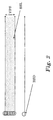
- Figure 2 depicts the general approach of the invention.
- VPS is the vertical pixel size
- SSL is the sub-pixel size
- BSD is the beam spot diameter.
- the vertical pixel is broken down to sub-pixels, each having a width smaller than the spot size.
- the image is generated by scanning a successive number of images of the object, while each image has a different vertical shift. All the images can then be averaged together.
- the vertical distance between two scanned lines must be smaller than the actual beam spot size, by a specific ratio. This is achieved, according to the present invention, by carrying out the sub-pixel shift of each averaged image, relative to the previous one. Since the resolution is limited in this case by the pixel size, any subpixel shift will not degrade the resolution. According to a preferred embodiment of the invention the required subpixel shift is computed separately for each field of view in order to optimize the image reconstruction of the object.
- the scan and display ordering can be selected from several options. The simplest method would be to scan the lines successively in order from top to bottom, and display the obtained lines in real time. This, however, causes a flicker phenomena, since the sample is sampled differently in each scan. Such a flicker may irritate the operator. Thus, one solution is to blank the display until all the images have been acquired and averaged.
- the scanning order can be set to be random or semi random. By semi-random is meant that constraints are imposed on the random generation (e.g., no three successive lines in a row). It is the inventor's experience that using a random sub-pixel vertical shift avoids the flicker phenomena even if the images are displayed in real time.
- This method applies when the number of frames to be averaged is known before the scanning operation starts. There are two parameters involved in this calculation.
- the number of subpixel shifts is equal to the following: maximum (integer(2 X pixelsize/spot diameter), number of frames) and the actual vertical distance of the subpixel shift is given by Vertical pixel size Number of subpixel shifts
- the subpixel shift is carried out in a cyclic manner. Once the accumulated vertical shift is equal to the vertical distance between the original scanned lines, the subpixel shift of the next image is set again to zero.
- Correcting the aliasing error with the above method during a continuous scan may induce a flicker in the screen due to the fact that the object is being sampled in a different way at each frame.
- the flicker it is required to create the subpixel vertical shifts in a random manner and not in a successive order.
- a photoresist on a silicon wafer was scanned using a GEMINI LEO, U.K. apparatus, equipped with a digital scanner.
- the digital scanner was an in-house developed scanner, but any suitable digital scanner can be used instead. This scanner was used in all cases.
- the image obtained without any anti-aliasing correction is shown in Fig. 1A, which exhibits marked aliasing errors. These are especially obvious at the fringes of the dark squares in the image, which are unequal in their intensity (Moire fringes). As a result, the squares appear contorted.
- Fig. 1B shows that the aliasing errors described above have been substantially corrected.
- FIG. 3A shows the operation of the system and its inputs
- Fig. 3B illustrates the steps after the image is detected at the detector.
- a host which is typically a PC or other computer, receives operating instructions, either directly from the operator, or in pre-programmed form. These instructions include, for example, the type of average employed, the number of frames desired, the image size in pixels, the FOV and scan rate. From this input the host generates appropriate values for the number of pixels, the number of lines, the pixel time and the sub-pixel shift.
- the generation method of these values will be apparent to the skilled person from the above description, and is therefore not discussed herein in detail, for the sake of brevity.
- the operating instructions generated by the host are fed to the digital scanner, which translates them in X and Y movements of the scanning beam (schematically shown in the figure), which are further handled by system elements such as the scan amplifier and the attenuator, which are known in the art and therefore not discussed herein in detail.
- the image is generated by the stream of secondary or back-scattered electrons, which are detected by a detector, as schematically shown in Fig. 3B. These are translated into images in a manner known per se , and then, through a video frame grabber, are fed to an image processor which averages the pixels and sends the resulting image to display means and/or to printing means, to generate images such as those shown in Fig. 1.
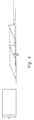
- Fig. 4 schematically illustrates the shift in the Y direction of the scanned signal with time. This results in progressive adjacent outputs, as shown in the figure.
- the line indicated as "VB” in the figure, is the well known Vertical Blank.
- rotated scan is meant that the scan axes do not coincide with the beam deflector axes, a scanning method known per s e. That is, generally the scan line in the x-direction is parallel to the virtual line connecting the x-scan deflectors, while the scan in the y-direction is parallel to the virtual line connecting the y-scan deflectors. In this way, the output of the scanner corresponds exactly to the axes defined by the physical deflectors. On the other hand, the scan in x-direction can be rotated, so that the axes of the image do not coincide with the actual axes of the deflectors.
Landscapes
- Chemical & Material Sciences (AREA)
- Analytical Chemistry (AREA)
- Engineering & Computer Science (AREA)
- Computer Vision & Pattern Recognition (AREA)
- Image Processing (AREA)
- Microscoopes, Condenser (AREA)
Applications Claiming Priority (2)
| Application Number | Priority Date | Filing Date | Title |
|---|---|---|---|
| US09/158,826 US6194718B1 (en) | 1998-09-23 | 1998-09-23 | Method for reducing aliasing effects in scanning beam microscopy |
| US158826 | 1998-09-23 |
Publications (3)
| Publication Number | Publication Date |
|---|---|
| EP0993019A2 true EP0993019A2 (de) | 2000-04-12 |
| EP0993019A3 EP0993019A3 (de) | 2001-03-21 |
| EP0993019B1 EP0993019B1 (de) | 2005-05-25 |
Family
ID=22569881
Family Applications (1)
| Application Number | Title | Priority Date | Filing Date |
|---|---|---|---|
| EP99118816A Expired - Lifetime EP0993019B1 (de) | 1998-09-23 | 1999-09-23 | Verfahren zur Reduzierung von Artefakterscheinungen in der Raster-Elektronenmikroskopie |
Country Status (3)
| Country | Link |
|---|---|
| US (1) | US6194718B1 (de) |
| EP (1) | EP0993019B1 (de) |
| DE (1) | DE69925430T2 (de) |
Cited By (8)
| Publication number | Priority date | Publication date | Assignee | Title |
|---|---|---|---|---|
| FR2820151A1 (fr) * | 2001-01-30 | 2002-08-02 | X Ion | Procede et systeme de balayage d'un faisceau d'ions sur un substrat, ainsi qu'application a la formation d'oxyde de grille ou de nanocristaux |
| US6633831B2 (en) | 2000-09-20 | 2003-10-14 | Kla Tencor Technologies | Methods and systems for determining a critical dimension and a thin film characteristic of a specimen |
| US6673637B2 (en) | 2000-09-20 | 2004-01-06 | Kla-Tencor Technologies | Methods and systems for determining a presence of macro defects and overlay of a specimen |
| US6694284B1 (en) | 2000-09-20 | 2004-02-17 | Kla-Tencor Technologies Corp. | Methods and systems for determining at least four properties of a specimen |
| US6782337B2 (en) | 2000-09-20 | 2004-08-24 | Kla-Tencor Technologies Corp. | Methods and systems for determining a critical dimension an a presence of defects on a specimen |
| US6812045B1 (en) | 2000-09-20 | 2004-11-02 | Kla-Tencor, Inc. | Methods and systems for determining a characteristic of a specimen prior to, during, or subsequent to ion implantation |
| US6891627B1 (en) | 2000-09-20 | 2005-05-10 | Kla-Tencor Technologies Corp. | Methods and systems for determining a critical dimension and overlay of a specimen |
| US7236847B2 (en) | 2002-01-16 | 2007-06-26 | Kla-Tencor Technologies Corp. | Systems and methods for closed loop defect reduction |
Families Citing this family (18)
| Publication number | Priority date | Publication date | Assignee | Title |
|---|---|---|---|---|
| US7349090B2 (en) | 2000-09-20 | 2008-03-25 | Kla-Tencor Technologies Corp. | Methods and systems for determining a property of a specimen prior to, during, or subsequent to lithography |
| US6919957B2 (en) | 2000-09-20 | 2005-07-19 | Kla-Tencor Technologies Corp. | Methods and systems for determining a critical dimension, a presence of defects, and a thin film characteristic of a specimen |
| US7130029B2 (en) | 2000-09-20 | 2006-10-31 | Kla-Tencor Technologies Corp. | Methods and systems for determining an adhesion characteristic and a thickness of a specimen |
| US7106425B1 (en) | 2000-09-20 | 2006-09-12 | Kla-Tencor Technologies Corp. | Methods and systems for determining a presence of defects and a thin film characteristic of a specimen |
| US6770867B2 (en) | 2001-06-29 | 2004-08-03 | Fei Company | Method and apparatus for scanned instrument calibration |
| WO2003005396A2 (en) * | 2001-01-26 | 2003-01-16 | Fei Company | Method and apparatus for scanned instrument calibration |
| US7227984B2 (en) | 2003-03-03 | 2007-06-05 | Kla-Tencor Technologies Corporation | Method and apparatus for identifying defects in a substrate surface by using dithering to reconstruct under-sampled images |
| DE102004034974A1 (de) * | 2004-07-16 | 2006-02-16 | Carl Zeiss Jena Gmbh | Verfahren zur bildlichen Erfassung von Objekten mittels eines Lichtrastermikroskopes mit punktförmiger Lichtquellenverteilung |
| DE102004034963A1 (de) * | 2004-07-16 | 2006-02-16 | Carl Zeiss Jena Gmbh | Verfahren zur bildlichen Erfassung von Objekten mittels eines Lichtrastermikroskopes |
| DE102004034951A1 (de) * | 2004-07-16 | 2006-02-02 | Carl Zeiss Jena Gmbh | Verfahren zur bildlichen Erfassung von Objekten mittels eines Lichtrastermikrokopes mit linienförmiger Abtastung |
| JP2006203463A (ja) * | 2005-01-19 | 2006-08-03 | Matsushita Electric Ind Co Ltd | 画像表示方法、画像撮像方法、及び画像合成方法 |
| WO2011119678A2 (en) | 2010-03-23 | 2011-09-29 | California Institute Of Technology | Super resolution optofluidic microscopes for 2d and 3d imaging |
| US9426429B2 (en) | 2010-10-26 | 2016-08-23 | California Institute Of Technology | Scanning projective lensless microscope system |
| US9569664B2 (en) * | 2010-10-26 | 2017-02-14 | California Institute Of Technology | Methods for rapid distinction between debris and growing cells |
| US9643184B2 (en) * | 2010-10-26 | 2017-05-09 | California Institute Of Technology | e-Petri dishes, devices, and systems having a light detector for sampling a sequence of sub-pixel shifted projection images |
| WO2012119094A2 (en) | 2011-03-03 | 2012-09-07 | California Institute Of Technology | Light guided pixel |
| JP6548542B2 (ja) * | 2015-09-29 | 2019-07-24 | 株式会社ホロン | Sem画像取得装置およびsem画像取得方法 |
| JP7077260B2 (ja) * | 2019-03-22 | 2022-05-30 | 株式会社日立ハイテク | 電子ビーム装置及び画像処理方法 |
Family Cites Families (9)
| Publication number | Priority date | Publication date | Assignee | Title |
|---|---|---|---|---|
| US3767926A (en) * | 1972-05-08 | 1973-10-23 | American Optical Corp | Field emission scanning microscope display |
| DE2635674C3 (de) * | 1976-08-07 | 1978-10-26 | Dr.-Ing. Rudolf Hell Gmbh, 2300 Kiel | Verfahren zur zeilenfreien Bildaufzeichnung |
| US4811409A (en) | 1985-09-12 | 1989-03-07 | Insystems, Inc. | Method and apparatus for detecting defect information in a holographic image pattern |
| US4907287A (en) * | 1985-10-16 | 1990-03-06 | Hitachi, Ltd. | Image correction system for scanning electron microscope |
| US5299308A (en) * | 1990-02-28 | 1994-03-29 | Ricoh Company, Ltd. | Graphic data processing apparatus for producing a tone for an edge pixel and reducing aliasing effects |
| JP3071229B2 (ja) * | 1990-04-09 | 2000-07-31 | 株式会社リコー | 図形処理装置 |
| US5717204A (en) * | 1992-05-27 | 1998-02-10 | Kla Instruments Corporation | Inspecting optical masks with electron beam microscopy |
| US6005682A (en) * | 1995-06-07 | 1999-12-21 | Xerox Corporation | Resolution enhancement by multiple scanning with a low-resolution, two-dimensional sensor array |
| US5925875A (en) * | 1996-04-26 | 1999-07-20 | Lockheed Martin Ir Imaging Systems | Apparatus and method for compensating for fixed pattern noise in planar arrays |
-
1998
- 1998-09-23 US US09/158,826 patent/US6194718B1/en not_active Expired - Lifetime
-
1999
- 1999-09-23 DE DE69925430T patent/DE69925430T2/de not_active Expired - Lifetime
- 1999-09-23 EP EP99118816A patent/EP0993019B1/de not_active Expired - Lifetime
Cited By (12)
| Publication number | Priority date | Publication date | Assignee | Title |
|---|---|---|---|---|
| US6633831B2 (en) | 2000-09-20 | 2003-10-14 | Kla Tencor Technologies | Methods and systems for determining a critical dimension and a thin film characteristic of a specimen |
| US6673637B2 (en) | 2000-09-20 | 2004-01-06 | Kla-Tencor Technologies | Methods and systems for determining a presence of macro defects and overlay of a specimen |
| US6694284B1 (en) | 2000-09-20 | 2004-02-17 | Kla-Tencor Technologies Corp. | Methods and systems for determining at least four properties of a specimen |
| US6782337B2 (en) | 2000-09-20 | 2004-08-24 | Kla-Tencor Technologies Corp. | Methods and systems for determining a critical dimension an a presence of defects on a specimen |
| US6806951B2 (en) | 2000-09-20 | 2004-10-19 | Kla-Tencor Technologies Corp. | Methods and systems for determining at least one characteristic of defects on at least two sides of a specimen |
| US6812045B1 (en) | 2000-09-20 | 2004-11-02 | Kla-Tencor, Inc. | Methods and systems for determining a characteristic of a specimen prior to, during, or subsequent to ion implantation |
| US6818459B2 (en) | 2000-09-20 | 2004-11-16 | Kla-Tencor Technologies Corp. | Methods and systems for determining a presence of macro defects and overlay of a specimen |
| US6829559B2 (en) | 2000-09-20 | 2004-12-07 | K.L.A.-Tencor Technologies | Methods and systems for determining a presence of macro and micro defects on a specimen |
| US6891627B1 (en) | 2000-09-20 | 2005-05-10 | Kla-Tencor Technologies Corp. | Methods and systems for determining a critical dimension and overlay of a specimen |
| US6891610B2 (en) | 2000-09-20 | 2005-05-10 | Kla-Tencor Technologies Corp. | Methods and systems for determining an implant characteristic and a presence of defects on a specimen |
| FR2820151A1 (fr) * | 2001-01-30 | 2002-08-02 | X Ion | Procede et systeme de balayage d'un faisceau d'ions sur un substrat, ainsi qu'application a la formation d'oxyde de grille ou de nanocristaux |
| US7236847B2 (en) | 2002-01-16 | 2007-06-26 | Kla-Tencor Technologies Corp. | Systems and methods for closed loop defect reduction |
Also Published As
| Publication number | Publication date |
|---|---|
| US6194718B1 (en) | 2001-02-27 |
| DE69925430D1 (de) | 2005-06-30 |
| DE69925430T2 (de) | 2006-02-02 |
| EP0993019A3 (de) | 2001-03-21 |
| EP0993019B1 (de) | 2005-05-25 |
Similar Documents
| Publication | Publication Date | Title |
|---|---|---|
| EP0993019B1 (de) | Verfahren zur Reduzierung von Artefakterscheinungen in der Raster-Elektronenmikroskopie | |
| CN115053320B (zh) | 多光束数字扫描以及图像获取 | |
| JP4426871B2 (ja) | Fib/sem複合装置の画像ノイズ除去 | |
| CN108027501B (zh) | 多束扫描电子显微镜系统中噪声减少的方法及系统 | |
| JP4512471B2 (ja) | 走査型電子顕微鏡及び半導体検査システム | |
| US7598492B1 (en) | Charged particle microscopy using super resolution | |
| US8125518B2 (en) | Scanning electron microscope | |
| US7982186B2 (en) | Method and apparatus for obtaining images by raster scanning charged particle beam over patterned substrate on a continuous mode stage | |
| US10614998B2 (en) | Charge reduction by digital image correlation | |
| JP7232326B2 (ja) | 粒子顕微鏡を用いる画像記録方法 | |
| JP3112503B2 (ja) | 荷電ビームを用いた画面処理方法及び荷電ビーム顕微鏡装置 | |
| TWI742524B (zh) | 電子束裝置及圖像處理方法 | |
| JPH11345585A (ja) | 電子ビームによる検査装置および検査方法 | |
| JP7576592B2 (ja) | 荷電粒子線装置および画像取得方法 | |
| Downing | Automatic focus correction for spot-scan imaging of tilted specimens | |
| TW202219499A (zh) | 圖像修正裝置、圖案檢查裝置及圖像修正方法 | |
| TWI867659B (zh) | 校正帶電粒子束掃描樣本時的影像誤差的方法、裝置和電腦程式 | |
| US20260100325A1 (en) | Dark correction for long term acquisition | |
| US20250166963A1 (en) | Method and System for Imaging a Sample | |
| EP4632787A1 (de) | Verfahren zur erzeugung einer serie von kippbildern einer probe in mehreren neigungswinkeln | |
| TW200425714A (en) | Method and apparatus for image formation from scan data, and control of a scanning apparatus for the same | |
| JP3790629B2 (ja) | 走査型荷電粒子ビーム装置及び走査型荷電粒子ビーム装置の動作方法 | |
| Oho et al. | An improved scanning method based on characteristics of the human visual system for scanning electron microscopy | |
| JPH0574402A (ja) | 走査電子顕微鏡 | |
| JP2021043127A (ja) | パターン検査装置およびパターン検査方法 |
Legal Events
| Date | Code | Title | Description |
|---|---|---|---|
| PUAI | Public reference made under article 153(3) epc to a published international application that has entered the european phase |
Free format text: ORIGINAL CODE: 0009012 |
|
| AK | Designated contracting states |
Kind code of ref document: A2 Designated state(s): DE FR GB IT NL |
|
| AX | Request for extension of the european patent |
Free format text: AL;LT;LV;MK;RO;SI |
|
| PUAL | Search report despatched |
Free format text: ORIGINAL CODE: 0009013 |
|
| AK | Designated contracting states |
Kind code of ref document: A3 Designated state(s): AT BE CH CY DE DK ES FI FR GB GR IE IT LI LU MC NL PT SE |
|
| AX | Request for extension of the european patent |
Free format text: AL;LT;LV;MK;RO;SI |
|
| 17P | Request for examination filed |
Effective date: 20010831 |
|
| AKX | Designation fees paid |
Free format text: DE FR GB IT NL |
|
| 17Q | First examination report despatched |
Effective date: 20020521 |
|
| GRAP | Despatch of communication of intention to grant a patent |
Free format text: ORIGINAL CODE: EPIDOSNIGR1 |
|
| GRAP | Despatch of communication of intention to grant a patent |
Free format text: ORIGINAL CODE: EPIDOSNIGR1 |
|
| GRAS | Grant fee paid |
Free format text: ORIGINAL CODE: EPIDOSNIGR3 |
|
| GRAA | (expected) grant |
Free format text: ORIGINAL CODE: 0009210 |
|
| AK | Designated contracting states |
Kind code of ref document: B1 Designated state(s): DE FR GB IT NL |
|
| PG25 | Lapsed in a contracting state [announced via postgrant information from national office to epo] |
Ref country code: NL Free format text: LAPSE BECAUSE OF FAILURE TO SUBMIT A TRANSLATION OF THE DESCRIPTION OR TO PAY THE FEE WITHIN THE PRESCRIBED TIME-LIMIT Effective date: 20050525 Ref country code: IT Free format text: LAPSE BECAUSE OF FAILURE TO SUBMIT A TRANSLATION OF THE DESCRIPTION OR TO PAY THE FEE WITHIN THE PRESCRIBED TIME-LIMIT;WARNING: LAPSES OF ITALIAN PATENTS WITH EFFECTIVE DATE BEFORE 2007 MAY HAVE OCCURRED AT ANY TIME BEFORE 2007. THE CORRECT EFFECTIVE DATE MAY BE DIFFERENT FROM THE ONE RECORDED. Effective date: 20050525 |
|
| REG | Reference to a national code |
Ref country code: GB Ref legal event code: FG4D |
|
| REF | Corresponds to: |
Ref document number: 69925430 Country of ref document: DE Date of ref document: 20050630 Kind code of ref document: P |
|
| PG25 | Lapsed in a contracting state [announced via postgrant information from national office to epo] |
Ref country code: GB Free format text: LAPSE BECAUSE OF NON-PAYMENT OF DUE FEES Effective date: 20050923 |
|
| NLV1 | Nl: lapsed or annulled due to failure to fulfill the requirements of art. 29p and 29m of the patents act | ||
| ET | Fr: translation filed | ||
| PLBE | No opposition filed within time limit |
Free format text: ORIGINAL CODE: 0009261 |
|
| STAA | Information on the status of an ep patent application or granted ep patent |
Free format text: STATUS: NO OPPOSITION FILED WITHIN TIME LIMIT |
|
| 26N | No opposition filed |
Effective date: 20060228 |
|
| GBPC | Gb: european patent ceased through non-payment of renewal fee |
Effective date: 20050923 |
|
| PGFP | Annual fee paid to national office [announced via postgrant information from national office to epo] |
Ref country code: FR Payment date: 20130826 Year of fee payment: 15 |
|
| PGFP | Annual fee paid to national office [announced via postgrant information from national office to epo] |
Ref country code: DE Payment date: 20130930 Year of fee payment: 15 |
|
| REG | Reference to a national code |
Ref country code: DE Ref legal event code: R119 Ref document number: 69925430 Country of ref document: DE |
|
| REG | Reference to a national code |
Ref country code: FR Ref legal event code: ST Effective date: 20150529 |
|
| PG25 | Lapsed in a contracting state [announced via postgrant information from national office to epo] |
Ref country code: DE Free format text: LAPSE BECAUSE OF NON-PAYMENT OF DUE FEES Effective date: 20150401 |
|
| PG25 | Lapsed in a contracting state [announced via postgrant information from national office to epo] |
Ref country code: FR Free format text: LAPSE BECAUSE OF NON-PAYMENT OF DUE FEES Effective date: 20140930 |