EP0993052A2 - Cellule solaire spatiale - Google Patents
Cellule solaire spatiale Download PDFInfo
- Publication number
- EP0993052A2 EP0993052A2 EP99118963A EP99118963A EP0993052A2 EP 0993052 A2 EP0993052 A2 EP 0993052A2 EP 99118963 A EP99118963 A EP 99118963A EP 99118963 A EP99118963 A EP 99118963A EP 0993052 A2 EP0993052 A2 EP 0993052A2
- Authority
- EP
- European Patent Office
- Prior art keywords
- solar cell
- back surface
- semiconductor substrate
- openings
- space solar
- Prior art date
- Legal status (The legal status is an assumption and is not a legal conclusion. Google has not performed a legal analysis and makes no representation as to the accuracy of the status listed.)
- Granted
Links
Images



Classifications
-
- H—ELECTRICITY
- H10—SEMICONDUCTOR DEVICES; ELECTRIC SOLID-STATE DEVICES NOT OTHERWISE PROVIDED FOR
- H10F—INORGANIC SEMICONDUCTOR DEVICES SENSITIVE TO INFRARED RADIATION, LIGHT, ELECTROMAGNETIC RADIATION OF SHORTER WAVELENGTH OR CORPUSCULAR RADIATION
- H10F77/00—Constructional details of devices covered by this subclass
- H10F77/20—Electrodes
- H10F77/206—Electrodes for devices having potential barriers
- H10F77/211—Electrodes for devices having potential barriers for photovoltaic cells
-
- H—ELECTRICITY
- H10—SEMICONDUCTOR DEVICES; ELECTRIC SOLID-STATE DEVICES NOT OTHERWISE PROVIDED FOR
- H10F—INORGANIC SEMICONDUCTOR DEVICES SENSITIVE TO INFRARED RADIATION, LIGHT, ELECTROMAGNETIC RADIATION OF SHORTER WAVELENGTH OR CORPUSCULAR RADIATION
- H10F10/00—Individual photovoltaic cells, e.g. solar cells
- H10F10/10—Individual photovoltaic cells, e.g. solar cells having potential barriers
- H10F10/14—Photovoltaic cells having only PN homojunction potential barriers
-
- H—ELECTRICITY
- H10—SEMICONDUCTOR DEVICES; ELECTRIC SOLID-STATE DEVICES NOT OTHERWISE PROVIDED FOR
- H10F—INORGANIC SEMICONDUCTOR DEVICES SENSITIVE TO INFRARED RADIATION, LIGHT, ELECTROMAGNETIC RADIATION OF SHORTER WAVELENGTH OR CORPUSCULAR RADIATION
- H10F77/00—Constructional details of devices covered by this subclass
- H10F77/40—Optical elements or arrangements
- H10F77/42—Optical elements or arrangements directly associated or integrated with photovoltaic cells, e.g. light-reflecting means or light-concentrating means
- H10F77/48—Back surface reflectors [BSR]
-
- Y—GENERAL TAGGING OF NEW TECHNOLOGICAL DEVELOPMENTS; GENERAL TAGGING OF CROSS-SECTIONAL TECHNOLOGIES SPANNING OVER SEVERAL SECTIONS OF THE IPC; TECHNICAL SUBJECTS COVERED BY FORMER USPC CROSS-REFERENCE ART COLLECTIONS [XRACs] AND DIGESTS
- Y02—TECHNOLOGIES OR APPLICATIONS FOR MITIGATION OR ADAPTATION AGAINST CLIMATE CHANGE
- Y02E—REDUCTION OF GREENHOUSE GAS [GHG] EMISSIONS, RELATED TO ENERGY GENERATION, TRANSMISSION OR DISTRIBUTION
- Y02E10/00—Energy generation through renewable energy sources
- Y02E10/50—Photovoltaic [PV] energy
- Y02E10/52—PV systems with concentrators
-
- Y—GENERAL TAGGING OF NEW TECHNOLOGICAL DEVELOPMENTS; GENERAL TAGGING OF CROSS-SECTIONAL TECHNOLOGIES SPANNING OVER SEVERAL SECTIONS OF THE IPC; TECHNICAL SUBJECTS COVERED BY FORMER USPC CROSS-REFERENCE ART COLLECTIONS [XRACs] AND DIGESTS
- Y02—TECHNOLOGIES OR APPLICATIONS FOR MITIGATION OR ADAPTATION AGAINST CLIMATE CHANGE
- Y02E—REDUCTION OF GREENHOUSE GAS [GHG] EMISSIONS, RELATED TO ENERGY GENERATION, TRANSMISSION OR DISTRIBUTION
- Y02E10/00—Energy generation through renewable energy sources
- Y02E10/50—Photovoltaic [PV] energy
- Y02E10/547—Monocrystalline silicon PV cells
-
- Y—GENERAL TAGGING OF NEW TECHNOLOGICAL DEVELOPMENTS; GENERAL TAGGING OF CROSS-SECTIONAL TECHNOLOGIES SPANNING OVER SEVERAL SECTIONS OF THE IPC; TECHNICAL SUBJECTS COVERED BY FORMER USPC CROSS-REFERENCE ART COLLECTIONS [XRACs] AND DIGESTS
- Y10—TECHNICAL SUBJECTS COVERED BY FORMER USPC
- Y10S—TECHNICAL SUBJECTS COVERED BY FORMER USPC CROSS-REFERENCE ART COLLECTIONS [XRACs] AND DIGESTS
- Y10S136/00—Batteries: thermoelectric and photoelectric
- Y10S136/291—Applications
- Y10S136/292—Space - satellite
Definitions
- the present invention relates to a space solar cell, and more particularly to a space solar cell (solar cell for space application) such as a space silicon solar cell which has good electrical output power characteristics and is suitably used under the environment of outer space.
- a space solar cell solar cell for space application
- space silicon solar cell which has good electrical output power characteristics and is suitably used under the environment of outer space.
- a silicon solar cell is widely used as a solar cell that converts light energy to electric energy.
- Such a silicon solar cell is used also under the environment of outer space such as in an artificial satellite.
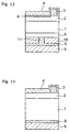
- Fig. 14 shows an example of a conventional silicon solar cell.
- This is referred to as BSR (back surface reflector) structure, where an N + -type diffusion layer 2 is formed on a light receiving surface located in a front surface of a 200 ⁇ m thick P-type silicon substrate 1 by thermal diffusion of an N-type impurity ions for taking in the carriers generated by the light energy, and a light-receiving surface electrode 3 is formed in a comb-teeth shape on the N + -type diffusion layer 2 for taking out the generated electricity. Further, the N + -type diffusion layer 2 and the light-receiving surface electrode 3 are covered with an anti-reflection film 4 for reducing a surface reflection of incident light.
- BSR back surface reflector
- a BSR electrode 5 is formed on the back surface of the silicon substrate 1 for improving the amount of generated carriers by increasing an optical path length by reflecting a long-wavelength light that escapes away from the back surface of the solar cell.
- a back surface electrode 6 is formed over an entire surface of the BSR electrode 5 for taking out the generated electricity. In the solar cell of this structure, a conversion efficiency is increased by allowing the light reaching the back surface of the silicon substrate 1 to be reflected by the BSR electrode 5 to take out an energy of the carries generated around the back surface effectively as an electric power.
- a solar cell with further increased conversion efficiency is shown in Fig. 15 and is referred to as an NRS/BSF (non-reflective surface/back surface field) structure, where a light-receiving surface of a 100 ⁇ m thick P-type silicon substrate 1 is formed into a non-reflection configuration 7 with numerous small inverted-pyramid recesses to reduce the surface reflection of solar light by multiple reflection.
- NRS structure non-reflective surface/back surface field
- an N + -type diffusion layer 2 is formed on a light receiving surface side of the P-type silicon substrate 1
- a front surface oxide film 8 is formed as a front surface dielectric layer on the N + -type diffusion layer 2.
- a light-receiving surface electrode 3 having a comb-teeth shape is connected to the N + -type diffusion layer 2 via openings formed in the oxide film 8. Further, the oxide film 8 and the light-receiving surface electrode 3 are covered with an anti-reflection film 4 for reducing the surface reflection of incident light.
- a P + -type diffusion layer 9 is formed on a back surface side of the silicon substrate 1 for allowing the carries generated in the silicon substrate 1 to move towards the N + -type diffusion layer (BSF structure).
- a back surface oxide film 10 is formed as a back surface dielectric layer on the P + -type diffusion layer 9.
- the BSR electrode 5 and the back surface electrode 6 are electrically connected to the P + -type diffusion layer 9 via a plurality of openings 11 formed in the oxide film 10.
- An internal electric field is formed by the P + -type diffusion layer 9, and the carriers generated near the back surface of the silicon substrate 1 are accelerated by this electric field, whereby recombination of the carriers is prevented and the energy of the carriers can be taken out effectively as an electric power.
- the photosensitivity to a long-wavelength light increases to improve the conversion efficiency.
- the solar cell utilizing a silicon substrate has a high conversion efficiency and is inexpensive, so that there has been a great demand for this type of a solar cell.
- a further improvement of output power is required in recent years and an improvement of an electric output power has been demanded. Therefore, an improvement of the output power must be achieved also in the solar cell having the above-mentioned structure.
- a back surface dielectric layer may be formed on a back surface of a silicon substrate to reduce the recombination, at the back surface, of carriers generated by the light energy, whereby the electric output power can be improved.
- a solar cell is disclosed, for example, in Japanese Unexamined Patent Publications No. HEI 04(1992)-274374 and No. HEI 06(1994)-169096.
- the back surface dielectric layer is already formed on the back surface of the silicon substrate.
- "Conference Record” 21th IEEE, Photovoltaic Specialists Conference, Florida, May 1990, pp. 333-335 proposes a technique in which the substrate includes a plurality of locally-formed P + layers and a silicon oxide film is used as the back dielectric layer.
- Japanese Unexamined Patent Publication No. HEI 04(1992)-15963 discloses a solar cell in which a special arrangement of diffusion layers is provided to increase the conversion efficiency.
- the present invention has been made in view of these circumstances, and the purpose thereof is to provide a space solar cell that can be suitably used under the environment of outer space by defining an aperture ratio in the back surface dielectric layer, thereby to improve the electric output power characteristics.
- the inventors of the present invention have found out that the loss in the electric power due to series resistance can be reduced and the electric output power characteristics can be improved by defining an aperture ratio (area ratio) to be within the range from 0.25 to 30%, the aperture ratio being a ratio of the area occupied by a plurality of openings formed in the back surface dielectric layer for establishing an electrical connection between the semiconductor substrate and the back surface electrode, relative to the area of the back surface of the semiconductor substrate. This finding has lead to the present invention.
- the present invention provides a space solar cell comprising a back surface electrode formed on a back surface opposite to a light receiving surface of a semiconductor substrate, and a dielectric layer formed between the back surface electrode and the semiconductor substrate, wherein a plurality of openings are formed in the dielectric layer for establishing an electrical connection between the back surface electrode and the semiconductor substrate, and a ratio of an area occupied by the openings relative to an area of the back surface is within a range from 0.25% to 30%.
- a dielectric layer is disposed between a back surface of a semiconductor substrate and a back surface electrode, and a plurality of openings are formed at an appropriate ratio in the dielectric layer.
- the area ratio of these openings maybe within the range from 0.25 to 30%, preferably within the range from 10 to 15%, more preferably a value of 12.25%. This reduces the series resistance and improves the electric output power characteristics.
- the reason why the area ratio occupied by the openings relative to the back surface of the semiconductor substrate is restricted to be within the range of 0.25 to 30% is as follows. If the ratio of the openings is larger than 30%, there will be a smaller effect produced by the dielectric layer for preventing recombination of carriers generated near the back surface of the semiconductor substrate; and moreover, since the solar light absorptivity ( ⁇ s) increases, the operating temperature will increase and the output power at the time of actual operation will decrease. On the other hand, if the ratio is smaller than 0.25%, the series resistance will increase and the electrical output power will decrease.
- the openings are preferably disposed with equal spacing.
- the openings preferably have a rectangular shape, more preferably a square shape.
- the openings may have a square shape with a side of about 70 ⁇ m and may be distributed at a pitch of about 200 ⁇ m.
- the openings may have a square shape with a side of about 30 ⁇ m and may be distributed at a pitch of about 300 ⁇ m.
- the openings are not limited to square-shaped dots, and may be circular or polygonal dots.
- the openings need not be arranged regularly, and may have a random configuration as long as the aperture ratio is within the defined range of 0.25 to 30%.
- the semiconductor substrate may be an N + -P-P + junction type semiconductor substrate including an N + -type diffusion layer formed on a light receiving side of a P-type silicon substrate and a P + -type diffusion layer formed on a back surface side of the P-type silicon substrate, or may be a P + -N-N + junction type semiconductor substrate including a P + -type diffusion layer formed on a light receiving side of an N-type silicon substrate and an N + -type diffusion layer formed on a back surface side of the N-type silicon substrate.
- the semiconductor substrate may be an N + -P junction type semiconductor substrate including an N + -type diffusion layer formed on a light-receiving side of a P-type silicon substrate, or may be a P + -N junction type semiconductor substrate including a P + -type diffusion layer formed on a light-receiving side of an N-type silicon substrate.
- the semiconductor substrate according to the present invention may have a non-reflection configuration (textures) in which the light-receiving surface is formed to have an uneven shape.
- textures non-reflection configuration
- the space solar cell according to the present invention may have any of a BSR structure, a BSFR (back surface field & reflector) structure, and an NRS/BSF structure.
- the dielectric layer may be an oxide film.
- the dielectric layer is not limited to an oxide film alone, and may be a nitride film. If the oxide film is to be used, the oxide film may be an SiO 2 film.
- the back surface electrode may include, for example, a three-layered metal laminate of Ti-Pd-Ag.
- the semiconductor substrate is preferably a silicon substrate in view of the photoelectric conversion efficiency and the production costs.
- the semiconductor substrate preferably has a thickness within the range from 50 to 250 ⁇ m in view of the initial electric output power characteristics and the electric output power characteristics after irradiation.
- the semiconductor substrate preferably has a resistivity within the range from 1 to 14 ⁇ cm in view of the initial electric output power characteristics and the electric output power characteristics after irradiation.
- Fig. 1 shows a solar cell having a BSR structure including a back surface dielectric layer (film) according to an embodiment of the present invention.
- the fundamental structure of this solar cell is an N + -P junction type, which is the same as that of the conventional solar cell shown in Fig. 14, wherein like numerals represent like elements in Fig. 14.
- a silicon substrate 1 having a thickness of 50 ⁇ m to 250 ⁇ m and a resistivity of 1 ⁇ cm to 14 ⁇ cm is used as the semiconductor substrate.
- a P-type single crystal silicon substrate 1 having a size of 36 x 69 mm, a thickness of 150 ⁇ m, and a resistivity of 2 ⁇ cm is used as the semiconductor substrate.
- a BSR electrode 5 made of a metal layer such as Al or Au and a back surface electrode 6 made of a metal layer such as Ti-Pd-Ag are laminated on a back surface of the silicon substrate 1.
- An oxide film 10 made of, for example, SiO 2 and acting as a back surface dielectric layer is formed between the BSR electrode 5 and the silicon substrate 1.
- a plurality of openings 11 which act as contact holes for establishing an electrical connection of the silicon substrate 1 with the BSR electrode 5 and the back surface electrode 6.
- the oxide film 10 is formed by thermal oxidation or the CVD method.
- the openings 11 are formed in the oxide film 10, for example, by using a photoetching technique.
- the area ratio of the openings 11 (aperture ratio) relative to the area of the back surface of the silicon substrate 1 is set to be within the range of 0.25% to 30%.
- the openings 11 are formed to have a square shape with a 70 ⁇ m side and are regularly arranged to be distributed at a pitch of 200 ⁇ m.
- the structure of the solar cell is an N + -P-P + junction type which is the same as the one shown in Fig. 15.
- a P-type single crystal silicon substrate 1 having a size of 36 mm x 69 mm, a thickness of 100 ⁇ m, and a resistivity of 2 ⁇ cm is used as the silicon substrate.
- a plurality of openings 11 are formed, for example, by using a photoetching technique in an oxide film 10 serving as a back surface dielectric layer.
- openings 11 are also used as contact holes for obtaining an electrical connection of a BSR electrode 5 being a metal layer made of Al and a back surface electrode 6 being a metal layer made of Ti-Pd-Ag formed on the oxide film 10, with a P + -type diffusion layer 9 on the back surface side of the silicon substrate 1.
- the openings 11 are formed to have a square shape with a 30 ⁇ m side and are regularly arranged to be distributed at a pitch of 300 ⁇ m.
- Figs. 4 and 8 show the change of the Pmax (maximum output power) relative to the aperture ratio in the oxide film 10 in the solar cells having the respective structures.
- Figs. 5 and 9 show the change of the solar light absorptivities ⁇ s relative to the aperture ratio in the oxide film 10 in the solar cells having the respective structures.
- Figs. 6 and 10 show the change of the operating temperatures Top relative to the aperture ratio in the oxide film 10 in the solar cells having the respective structures.
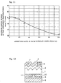
- Figs. 7 and 11 show the change of the maximum output power Pmax Top at the operating temperatures Top relative to the aperture ratio in the oxide film 10 in the solar cells having the respective structures.
- T op [ ⁇ s x S / ( ⁇ HF + ⁇ HB ) x ⁇ ] 1/4
- the improvement in the Pmax is considerable if the aperture ratio in the oxide film 10 is 0.25% or more and 30% or less.
- the reason why the Pmax decreases when the aperture ratio in the oxide film 10 is 0.25% or less is that, since the aperture ratio is small, the path for taking out the generated electricity is long to generate a series resistance that causes the FF to decrease. Also, the reason why the effect of improving the Pmax is small when the aperture ratio in the oxide film 10 is 30% or more is that the contact area between the silicon substrate 1 and the oxide film 10 for preventing the recombination of the carriers generated in the silicon substrate 1 is small and the Voc improvement obtained as a prevention effect is small.
- the solar light absorptivity ⁇ s increases and, as will be apparent from Figs. 6 and 19, the operating temperature also increases. Therefore, as shown in Figs. 7 and 11, if the aperture ratio in the oxide film 10 is 0.25% or more and 30% or less, the solar light absorptivity ⁇ s and the operating temperature do not increase so much, so that the improvement in the Pmax Top at the operating temperature is considerable.
- the electric output power characteristics tend to increase. Since the operating temperature is correlated with the solar light absorptivity of the solar cell, the solar light absorptivity can be decreased and the operating temperature can be lowered by forming a back surface dielectric layer on the back surface of the silicon substrate, whereby the effect of improvement in the electric output power characteristics increases to make the solar cell suitable for use under the environment of outer space that produces a limited heat-dissipating effect.
- the present invention is not limited to the above-mentioned embodiments and numerous changes and modifications can of course be made to the above-mentioned embodiments within the scope of the present invention.
- a P-type silicon substrate is used in this embodiment, an N-type silicon substrate can be used as well. If the N-type silicon substrate is used, the diffusion layer on the front surface side of the silicon substrate will be P-type and the diffusion layer on the back surface side of the silicon substrate will be N-type. In other words, a P + -N-N + junction type or P + -N junction type solar cell is provided.
- the semiconductor substrate constituting the P-N junction is not limited to a single crystal silicon substrate alone, so that polycrystal silicon or other materials can be used as well.
- the solar cell may have a structure in which a non-reflection configuration (textures) is formed on the light-receiving surface of the solar cell (in Fig. 12, a BSR structure is shown).
- the solar cell may have a structure in which the light-receiving surface is generally flat (in Fig. 13, a BSFR structure having a front surface oxide film is shown).
- the BSR electrode on the back surface may be omitted to allow the back surface electrode to be in direct contact with the dielectric layer.
- the back surface dielectric layer is not limited to an oxide film alone, and may be a nitride film.
- the openings in the back surface dielectric film need not be square-shaped dots, and may be circular or polygonal dots. Further, instead of regular arrangement, the openings may be randomly arranged as long as the aperture ratio is within the defined range of 0.25 to 30%.
- the electrode material is not limited to the above-mentioned metal alone.
- the aperture ratio of the back surface dielectric layer has been explained.
- explanation will be given on the thickness of the semiconductor substrate and the resistivity of the semiconductor substrate in the case where the aperture ratio in the back surface dielectric film is set to be 12.25% in order to adapt the solar cell of the present invention particularly for use under the environment of outer space.
- a solar cell to be used under the environment of outer space suffers from a large amount of irradiation in the outer space, so that the hardness against the radioactive rays is important.
- the relationship between the thickness of the semiconductor substrate and the radiation hardness was examined under a condition with the electron beam radiation amount of 1x10 15 e/cm 2 , which corresponds to 10 years in a geostationary orbit under the environment of outer space, using a solar cell having an NRS/BSF structure and a back surface dielectric layer aperture ratio of 12.25%.
- the semiconductor substrate of a solar cell for use under the environment of outer space preferably has a thickness of 50 to 250 ⁇ m in view of the endurance against the radioactive rays under the environment of outer space.
- the relationship between the resistivity of the semiconductor substrate and the radiation hardness was examined under a condition of 1 MeV electron 1 x 10 15 e/cm 2 irradiation, which corresponds to 10 years in a geostationary orbit under the environment of outer space, using a solar cell having a BSFR structure with the semiconductor substrate having a thickness of 100 ⁇ m and a back surface dielectric layer aperture ratio of 12.25%.
- the resistivity of the semiconductor substrate is preferably 1 to 14 ⁇ cm in order to use the solar cell under the environment of outer space.
- Resistivity of semiconductor substrate Initial electric Property (Pmax) Electric Property (Pmax) after irradiation of 1 MeV electrons with 1 x 10 15 e/cm 2 2 ⁇ cm 80.0 (mW) 53.6 (mW) 10 ⁇ cm 79.5 (mW) 55.7 (mW) 150 ⁇ cm 76.1 (mW) 54.8 (mW)
- the thickness of the semiconductor substrate is preferably as small as possible in view of the endurance against radioactive rays and the reduction of weight, because a thinner substrate leads to reduction of weight of an artificial satellite.
- the resistivity of the semiconductor substrate is preferably lower in view of the initial electrical output power characteristics but is preferably around 10 ⁇ cm in view of the endurance against irradiation. Therefore, it is necessary to select a semiconductor substrate having a resistivity that can ensure a predetermined minimum electrical output power at the last life stage of the artificial satellite, considering the amount of exposure of the artificial satellite to irradiation.
- a plurality of openings for establishing an electrical connection between the back surface electrode and the semiconductor substrate are formed in the dielectric layer which is provided on the back surface of the semiconductor substrate for improvement of the electrical output power characteristics.
- the openings are regularly arranged to be distributed with an equal spacing, the effect of providing the dielectric layer will be great to prevent recombination of the carriers, whereby the output power will increase and the conversion efficiency will be improved.
- the solar light absorptivity can be reduced, the operating temperature decreases and the maximum output power at the operating temperature is further improved. Therefore, a solar cell suitable for use under the environment of outer space can be provided.
- a space solar cell having a high output power and an excellent radiation hardness can be obtained by setting the thickness of the semiconductor substrate to be within the range of 50 to 250 ⁇ m and setting the resistivity of the semiconductor substrate to be within the range of 1 to 14 ⁇ cm.
Landscapes
- Photovoltaic Devices (AREA)
Applications Claiming Priority (2)
| Application Number | Priority Date | Filing Date | Title |
|---|---|---|---|
| JP27267898 | 1998-09-28 | ||
| JP27267898 | 1998-09-28 |
Publications (3)
| Publication Number | Publication Date |
|---|---|
| EP0993052A2 true EP0993052A2 (fr) | 2000-04-12 |
| EP0993052A3 EP0993052A3 (fr) | 2000-05-31 |
| EP0993052B1 EP0993052B1 (fr) | 2009-01-14 |
Family
ID=17517276
Family Applications (1)
| Application Number | Title | Priority Date | Filing Date |
|---|---|---|---|
| EP99118963A Expired - Lifetime EP0993052B1 (fr) | 1998-09-28 | 1999-09-27 | Cellule solaire spatiale |
Country Status (3)
| Country | Link |
|---|---|
| US (2) | US6229084B1 (fr) |
| EP (1) | EP0993052B1 (fr) |
| DE (1) | DE69940291D1 (fr) |
Families Citing this family (39)
| Publication number | Priority date | Publication date | Assignee | Title |
|---|---|---|---|---|
| US7907319B2 (en) | 1995-11-06 | 2011-03-15 | Qualcomm Mems Technologies, Inc. | Method and device for modulating light with optical compensation |
| WO1999052006A2 (fr) | 1998-04-08 | 1999-10-14 | Etalon, Inc. | Modulation interferometrique de rayonnement |
| US8928967B2 (en) | 1998-04-08 | 2015-01-06 | Qualcomm Mems Technologies, Inc. | Method and device for modulating light |
| EP0993052B1 (fr) * | 1998-09-28 | 2009-01-14 | Sharp Kabushiki Kaisha | Cellule solaire spatiale |
| WO2003007049A1 (fr) | 1999-10-05 | 2003-01-23 | Iridigm Display Corporation | Mems et structures photoniques |
| TW501286B (en) * | 2001-06-07 | 2002-09-01 | Ind Tech Res Inst | Polysilicon thin film solar cell substrate |
| US6660928B1 (en) | 2002-04-02 | 2003-12-09 | Essential Research, Inc. | Multi-junction photovoltaic cell |
| US7288825B2 (en) * | 2002-12-18 | 2007-10-30 | Noble Peak Vision Corp. | Low-noise semiconductor photodetectors |
| US7455787B2 (en) * | 2003-08-01 | 2008-11-25 | Sunpower Corporation | Etching of solar cell materials |
| US20050067667A1 (en) * | 2003-09-26 | 2005-03-31 | Goushcha Alexander O. | Fast silicon photodiodes with high back surface reflectance in a wavelength range close to the bandgap |
| US20050139253A1 (en) * | 2003-12-31 | 2005-06-30 | Korman Charles S. | Solar cell assembly for use in an outer space environment or a non-earth environment |
| US20050139256A1 (en) * | 2003-12-31 | 2005-06-30 | Korman Charles S. | Solar cell assembly for use in an outer space environment or a non-earth environment |
| US20050139255A1 (en) * | 2003-12-31 | 2005-06-30 | Korman Charles S. | Solar cell assembly for use in an outer space environment or a non-earth environment |
| US7916980B2 (en) | 2006-01-13 | 2011-03-29 | Qualcomm Mems Technologies, Inc. | Interconnect structure for MEMS device |
| US7915517B2 (en) * | 2006-08-16 | 2011-03-29 | Lau Po K | Bifacial photovoltaic devices |
| US20090078316A1 (en) * | 2007-09-24 | 2009-03-26 | Qualcomm Incorporated | Interferometric photovoltaic cell |
| US8129613B2 (en) * | 2008-02-05 | 2012-03-06 | Twin Creeks Technologies, Inc. | Photovoltaic cell comprising a thin lamina having low base resistivity and method of making |
| US8481845B2 (en) * | 2008-02-05 | 2013-07-09 | Gtat Corporation | Method to form a photovoltaic cell comprising a thin lamina |
| US8563352B2 (en) * | 2008-02-05 | 2013-10-22 | Gtat Corporation | Creation and translation of low-relief texture for a photovoltaic cell |
| EP2351097A2 (fr) * | 2008-10-23 | 2011-08-03 | Alta Devices, Inc. | Dispositif photovoltaïque |
| TW201031006A (en) * | 2008-10-23 | 2010-08-16 | Alta Devices Inc | Photovoltaic device with increased light trapping |
| US20120104460A1 (en) | 2010-11-03 | 2012-05-03 | Alta Devices, Inc. | Optoelectronic devices including heterojunction |
| WO2010048543A2 (fr) * | 2008-10-23 | 2010-04-29 | Alta Devices, Inc. | Couche mince d'absorbeur d'un dispositif photovoltaïque |
| CN102272516A (zh) | 2009-01-13 | 2011-12-07 | 高通Mems科技公司 | 大面积光面板及屏幕 |
| US8207443B2 (en) * | 2009-01-27 | 2012-06-26 | Applied Materials, Inc. | Point contacts for polysilicon emitter solar cell |
| WO2010104890A2 (fr) * | 2009-03-09 | 2010-09-16 | The University Of North Carolina At Charlotte | Amélioration du rendement des cellules solaires par gestion de la lumière |
| JP2010283339A (ja) * | 2009-05-02 | 2010-12-16 | Semiconductor Energy Lab Co Ltd | 光電変換装置及びその作製方法 |
| US20100326510A1 (en) * | 2009-06-27 | 2010-12-30 | Twin Creeks Technologies, Inc. | Thin semiconductor lamina adhered to a flexible substrate |
| US9691921B2 (en) | 2009-10-14 | 2017-06-27 | Alta Devices, Inc. | Textured metallic back reflector |
| US9768329B1 (en) | 2009-10-23 | 2017-09-19 | Alta Devices, Inc. | Multi-junction optoelectronic device |
| US9502594B2 (en) | 2012-01-19 | 2016-11-22 | Alta Devices, Inc. | Thin-film semiconductor optoelectronic device with textured front and/or back surface prepared from template layer and etching |
| US20150380576A1 (en) | 2010-10-13 | 2015-12-31 | Alta Devices, Inc. | Optoelectronic device with dielectric layer and method of manufacture |
| US11271128B2 (en) | 2009-10-23 | 2022-03-08 | Utica Leaseco, Llc | Multi-junction optoelectronic device |
| US20170141256A1 (en) | 2009-10-23 | 2017-05-18 | Alta Devices, Inc. | Multi-junction optoelectronic device with group iv semiconductor as a bottom junction |
| US8349626B2 (en) * | 2010-03-23 | 2013-01-08 | Gtat Corporation | Creation of low-relief texture for a photovoltaic cell |
| US11038080B2 (en) | 2012-01-19 | 2021-06-15 | Utica Leaseco, Llc | Thin-film semiconductor optoelectronic device with textured front and/or back surface prepared from etching |
| US9362443B2 (en) | 2013-03-13 | 2016-06-07 | Wafertech, Llc | Solar cell with absorber layer with three dimensional projections for energy harvesting, and method for forming the same |
| US9530908B2 (en) * | 2014-11-13 | 2016-12-27 | International Business Machines Corporation | Hybrid vapor phase-solution phase growth techniques for improved CZT(S,Se) photovoltaic device performance |
| GR20150100472A (el) * | 2015-10-30 | 2017-07-03 | Πανεπιστημιο Πατρων | Δισκια πολυκρυσταλλικου πυριτιου με διαμορφωμενες μικροδομες στις επιφανειες τους για την βελτιωση της ηλιακης απορροφησης |
Family Cites Families (10)
| Publication number | Priority date | Publication date | Assignee | Title |
|---|---|---|---|---|
| US3462311A (en) * | 1966-05-20 | 1969-08-19 | Globe Union Inc | Semiconductor device having improved resistance to radiation damage |
| US4355196A (en) | 1981-03-11 | 1982-10-19 | The United States Of America As Represented By The Administrator Of The National Aeronautics And Space Administration | Solar cell having improved back surface reflector |
| US5057163A (en) * | 1988-05-04 | 1991-10-15 | Astropower, Inc. | Deposited-silicon film solar cell |
| JPH07105519B2 (ja) * | 1989-10-03 | 1995-11-13 | シャープ株式会社 | 太陽電池セル |
| JPH0427434A (ja) | 1990-05-23 | 1992-01-30 | Mitsubishi Heavy Ind Ltd | メタノール改質用触媒 |
| JPH04274374A (ja) | 1991-02-28 | 1992-09-30 | Mitsubishi Electric Corp | 太陽電池及びその製造方法 |
| JP3203076B2 (ja) * | 1992-11-30 | 2001-08-27 | シャープ株式会社 | 宇宙用シリコン太陽電池 |
| JP3107287B2 (ja) * | 1996-03-25 | 2000-11-06 | 株式会社日立製作所 | 太陽電池 |
| JP3120762B2 (ja) | 1997-11-12 | 2000-12-25 | 日本電気株式会社 | 増幅器 |
| EP0993052B1 (fr) * | 1998-09-28 | 2009-01-14 | Sharp Kabushiki Kaisha | Cellule solaire spatiale |
-
1999
- 1999-09-27 EP EP99118963A patent/EP0993052B1/fr not_active Expired - Lifetime
- 1999-09-27 US US09/406,680 patent/US6229084B1/en not_active Expired - Lifetime
- 1999-09-27 DE DE69940291T patent/DE69940291D1/de not_active Expired - Lifetime
-
2001
- 2001-02-21 US US09/783,517 patent/US6403877B2/en not_active Expired - Lifetime
Also Published As
| Publication number | Publication date |
|---|---|
| EP0993052B1 (fr) | 2009-01-14 |
| US6403877B2 (en) | 2002-06-11 |
| US20010011553A1 (en) | 2001-08-09 |
| DE69940291D1 (de) | 2009-03-05 |
| EP0993052A3 (fr) | 2000-05-31 |
| US6229084B1 (en) | 2001-05-08 |
Similar Documents
| Publication | Publication Date | Title |
|---|---|---|
| US6403877B2 (en) | Space solar cell | |
| US4409422A (en) | High intensity solar cell | |
| US4332973A (en) | High intensity solar cell | |
| US4110122A (en) | High-intensity, solid-state-solar cell device | |
| US7208674B2 (en) | Solar cell having photovoltaic cells inclined at acute angle to each other | |
| US20090288702A1 (en) | Solar Cell and Solar Cell Module Using the Same | |
| US4516314A (en) | Method of making a high intensity solar cell | |
| US6617508B2 (en) | Solar cell having a front-mounted bypass diode | |
| EP1724840B1 (fr) | Cellule photoelectrique | |
| US6515217B1 (en) | Solar cell having a three-dimensional array of photovoltaic cells enclosed within an enclosure having reflective surfaces | |
| US4283589A (en) | High-intensity, solid-state solar cell | |
| GB2034973A (en) | Solar cell with multi-layer insulation | |
| CN101689571B (zh) | 太阳电池单元 | |
| US20050000566A1 (en) | Germanium solar cell and method for the production thereof | |
| US6162987A (en) | Monolithic interconnected module with a tunnel junction for enhanced electrical and optical performance | |
| US20160359447A1 (en) | Photovoltaic module | |
| JP2008243830A (ja) | シリコン薄膜,集積化された太陽電池,モジュール,及びその製造方法 | |
| KR20160138491A (ko) | 고전압 태양광 모듈 | |
| KR101868566B1 (ko) | 태양 전지 | |
| Fernández et al. | Back‐surface optimization of germanium TPV cells | |
| US4128732A (en) | Solar cell | |
| US4151005A (en) | Radiation hardened semiconductor photovoltaic generator | |
| Schwartz | Review of silicon solar cells for high concentrations | |
| US20160005910A1 (en) | Vertical multi-junction photovoltaic cell with reverse current limiting element | |
| JP3203076B2 (ja) | 宇宙用シリコン太陽電池 |
Legal Events
| Date | Code | Title | Description |
|---|---|---|---|
| PUAI | Public reference made under article 153(3) epc to a published international application that has entered the european phase |
Free format text: ORIGINAL CODE: 0009012 |
|
| AK | Designated contracting states |
Kind code of ref document: A2 Designated state(s): DE FR |
|
| AX | Request for extension of the european patent |
Free format text: AL;LT;LV;MK;RO;SI |
|
| PUAL | Search report despatched |
Free format text: ORIGINAL CODE: 0009013 |
|
| AK | Designated contracting states |
Kind code of ref document: A3 Designated state(s): AT BE CH CY DE DK ES FI FR GB GR IE IT LI LU MC NL PT SE |
|
| AX | Request for extension of the european patent |
Free format text: AL;LT;LV;MK;RO;SI |
|
| RIC1 | Information provided on ipc code assigned before grant |
Free format text: 7H 01L 31/068 A, 7H 01L 31/0224 B, 7H 01L 31/0236 B, 7H 01L 31/052 B |
|
| 17P | Request for examination filed |
Effective date: 20001010 |
|
| AKX | Designation fees paid |
Free format text: DE FR |
|
| 17Q | First examination report despatched |
Effective date: 20060213 |
|
| 17Q | First examination report despatched |
Effective date: 20060213 |
|
| GRAP | Despatch of communication of intention to grant a patent |
Free format text: ORIGINAL CODE: EPIDOSNIGR1 |
|
| GRAC | Information related to communication of intention to grant a patent modified |
Free format text: ORIGINAL CODE: EPIDOSCIGR1 |
|
| GRAS | Grant fee paid |
Free format text: ORIGINAL CODE: EPIDOSNIGR3 |
|
| GRAA | (expected) grant |
Free format text: ORIGINAL CODE: 0009210 |
|
| AK | Designated contracting states |
Kind code of ref document: B1 Designated state(s): DE FR |
|
| REF | Corresponds to: |
Ref document number: 69940291 Country of ref document: DE Date of ref document: 20090305 Kind code of ref document: P |
|
| PLBE | No opposition filed within time limit |
Free format text: ORIGINAL CODE: 0009261 |
|
| STAA | Information on the status of an ep patent application or granted ep patent |
Free format text: STATUS: NO OPPOSITION FILED WITHIN TIME LIMIT |
|
| 26N | No opposition filed |
Effective date: 20091015 |
|
| PGFP | Annual fee paid to national office [announced via postgrant information from national office to epo] |
Ref country code: DE Payment date: 20120919 Year of fee payment: 14 Ref country code: FR Payment date: 20120926 Year of fee payment: 14 |
|
| REG | Reference to a national code |
Ref country code: DE Ref legal event code: R119 Ref document number: 69940291 Country of ref document: DE Effective date: 20140401 |
|
| REG | Reference to a national code |
Ref country code: FR Ref legal event code: ST Effective date: 20140530 |
|
| PG25 | Lapsed in a contracting state [announced via postgrant information from national office to epo] |
Ref country code: FR Free format text: LAPSE BECAUSE OF NON-PAYMENT OF DUE FEES Effective date: 20130930 Ref country code: DE Free format text: LAPSE BECAUSE OF NON-PAYMENT OF DUE FEES Effective date: 20140401 |