EP0994973B1 - Vorrichtung und verfahren zur keimbildung und abscheidung von diamant mittels heissdraht-dc-plasma - Google Patents
Vorrichtung und verfahren zur keimbildung und abscheidung von diamant mittels heissdraht-dc-plasma Download PDFInfo
- Publication number
- EP0994973B1 EP0994973B1 EP98931851A EP98931851A EP0994973B1 EP 0994973 B1 EP0994973 B1 EP 0994973B1 EP 98931851 A EP98931851 A EP 98931851A EP 98931851 A EP98931851 A EP 98931851A EP 0994973 B1 EP0994973 B1 EP 0994973B1
- Authority
- EP
- European Patent Office
- Prior art keywords
- substrate
- filament
- filament array
- electrode
- grid electrode
- Prior art date
- Legal status (The legal status is an assumption and is not a legal conclusion. Google has not performed a legal analysis and makes no representation as to the accuracy of the status listed.)
- Expired - Lifetime
Links
- 239000010432 diamond Substances 0.000 title claims abstract description 117
- 229910003460 diamond Inorganic materials 0.000 title claims abstract description 117
- 238000000034 method Methods 0.000 title claims abstract description 55
- 230000008021 deposition Effects 0.000 title claims abstract description 27
- 238000010899 nucleation Methods 0.000 title abstract description 49
- 230000006911 nucleation Effects 0.000 title abstract description 45
- 239000000758 substrate Substances 0.000 claims abstract description 202
- 239000007789 gas Substances 0.000 claims abstract description 31
- 239000000376 reactant Substances 0.000 claims abstract description 17
- 238000003491 array Methods 0.000 claims abstract description 14
- 239000001257 hydrogen Substances 0.000 claims abstract description 14
- 229910052739 hydrogen Inorganic materials 0.000 claims abstract description 14
- UFHFLCQGNIYNRP-UHFFFAOYSA-N Hydrogen Chemical compound [H][H] UFHFLCQGNIYNRP-UHFFFAOYSA-N 0.000 claims abstract description 12
- 239000000203 mixture Substances 0.000 claims description 17
- 238000010438 heat treatment Methods 0.000 claims description 15
- 238000000605 extraction Methods 0.000 claims description 13
- 229930195733 hydrocarbon Natural products 0.000 claims description 8
- 150000002430 hydrocarbons Chemical class 0.000 claims description 8
- OKTJSMMVPCPJKN-UHFFFAOYSA-N Carbon Chemical compound [C] OKTJSMMVPCPJKN-UHFFFAOYSA-N 0.000 claims description 7
- 229910052799 carbon Inorganic materials 0.000 claims description 7
- 238000007740 vapor deposition Methods 0.000 claims description 6
- 238000001816 cooling Methods 0.000 claims description 5
- IJGRMHOSHXDMSA-UHFFFAOYSA-N Atomic nitrogen Chemical compound N#N IJGRMHOSHXDMSA-UHFFFAOYSA-N 0.000 claims description 4
- 229910052751 metal Inorganic materials 0.000 claims description 4
- 239000002184 metal Substances 0.000 claims description 4
- QVGXLLKOCUKJST-UHFFFAOYSA-N atomic oxygen Chemical compound [O] QVGXLLKOCUKJST-UHFFFAOYSA-N 0.000 claims description 2
- 238000005513 bias potential Methods 0.000 claims description 2
- 229910052736 halogen Inorganic materials 0.000 claims description 2
- 150000002367 halogens Chemical class 0.000 claims description 2
- 229910052757 nitrogen Inorganic materials 0.000 claims description 2
- 239000001301 oxygen Substances 0.000 claims description 2
- 229910052760 oxygen Inorganic materials 0.000 claims description 2
- 230000002194 synthesizing effect Effects 0.000 claims description 2
- 239000011261 inert gas Substances 0.000 claims 1
- 150000002500 ions Chemical class 0.000 abstract description 23
- 230000008569 process Effects 0.000 abstract description 15
- 239000002243 precursor Substances 0.000 abstract description 9
- 238000006748 scratching Methods 0.000 abstract description 4
- 230000002393 scratching effect Effects 0.000 abstract description 4
- 239000013078 crystal Substances 0.000 abstract description 3
- 210000002381 plasma Anatomy 0.000 description 56
- 239000010408 film Substances 0.000 description 22
- 238000000151 deposition Methods 0.000 description 17
- 238000004050 hot filament vapor deposition Methods 0.000 description 15
- VNWKTOKETHGBQD-UHFFFAOYSA-N methane Chemical compound C VNWKTOKETHGBQD-UHFFFAOYSA-N 0.000 description 15
- 238000005229 chemical vapour deposition Methods 0.000 description 11
- 238000000576 coating method Methods 0.000 description 9
- XUIMIQQOPSSXEZ-UHFFFAOYSA-N Silicon Chemical compound [Si] XUIMIQQOPSSXEZ-UHFFFAOYSA-N 0.000 description 8
- 238000013459 approach Methods 0.000 description 7
- 230000007935 neutral effect Effects 0.000 description 7
- 229910052710 silicon Inorganic materials 0.000 description 7
- 239000010703 silicon Substances 0.000 description 7
- 230000015572 biosynthetic process Effects 0.000 description 6
- 238000010586 diagram Methods 0.000 description 6
- 239000002245 particle Substances 0.000 description 6
- 238000005516 engineering process Methods 0.000 description 5
- 238000005268 plasma chemical vapour deposition Methods 0.000 description 5
- 238000012423 maintenance Methods 0.000 description 4
- 238000004544 sputter deposition Methods 0.000 description 4
- 238000006243 chemical reaction Methods 0.000 description 3
- 239000011248 coating agent Substances 0.000 description 3
- 238000013461 design Methods 0.000 description 3
- 238000009792 diffusion process Methods 0.000 description 3
- 239000012530 fluid Substances 0.000 description 3
- 238000004519 manufacturing process Methods 0.000 description 3
- 239000010453 quartz Substances 0.000 description 3
- 238000000926 separation method Methods 0.000 description 3
- VYPSYNLAJGMNEJ-UHFFFAOYSA-N silicon dioxide Inorganic materials O=[Si]=O VYPSYNLAJGMNEJ-UHFFFAOYSA-N 0.000 description 3
- 239000004215 Carbon black (E152) Substances 0.000 description 2
- YZCKVEUIGOORGS-UHFFFAOYSA-N Hydrogen atom Chemical compound [H] YZCKVEUIGOORGS-UHFFFAOYSA-N 0.000 description 2
- 238000001069 Raman spectroscopy Methods 0.000 description 2
- 238000004833 X-ray photoelectron spectroscopy Methods 0.000 description 2
- 230000009471 action Effects 0.000 description 2
- 230000008901 benefit Effects 0.000 description 2
- 230000001427 coherent effect Effects 0.000 description 2
- 230000008878 coupling Effects 0.000 description 2
- 238000010168 coupling process Methods 0.000 description 2
- 238000005859 coupling reaction Methods 0.000 description 2
- 150000002431 hydrogen Chemical class 0.000 description 2
- 239000012535 impurity Substances 0.000 description 2
- 230000001939 inductive effect Effects 0.000 description 2
- 238000012986 modification Methods 0.000 description 2
- 230000004048 modification Effects 0.000 description 2
- 238000012544 monitoring process Methods 0.000 description 2
- 238000000879 optical micrograph Methods 0.000 description 2
- 238000012545 processing Methods 0.000 description 2
- 239000003870 refractory metal Substances 0.000 description 2
- 238000000638 solvent extraction Methods 0.000 description 2
- 238000000992 sputter etching Methods 0.000 description 2
- 229910052715 tantalum Inorganic materials 0.000 description 2
- 229910052721 tungsten Inorganic materials 0.000 description 2
- 238000005524 ceramic coating Methods 0.000 description 1
- 230000007547 defect Effects 0.000 description 1
- 230000001627 detrimental effect Effects 0.000 description 1
- 238000011161 development Methods 0.000 description 1
- 230000005684 electric field Effects 0.000 description 1
- 230000008030 elimination Effects 0.000 description 1
- 238000003379 elimination reaction Methods 0.000 description 1
- 230000002708 enhancing effect Effects 0.000 description 1
- 238000001534 heteroepitaxy Methods 0.000 description 1
- 238000003780 insertion Methods 0.000 description 1
- 230000037431 insertion Effects 0.000 description 1
- 238000010849 ion bombardment Methods 0.000 description 1
- 239000000463 material Substances 0.000 description 1
- 230000008018 melting Effects 0.000 description 1
- 238000002844 melting Methods 0.000 description 1
- 230000003287 optical effect Effects 0.000 description 1
- 238000004321 preservation Methods 0.000 description 1
- 238000005086 pumping Methods 0.000 description 1
- 230000006798 recombination Effects 0.000 description 1
- 238000005215 recombination Methods 0.000 description 1
- 238000012552 review Methods 0.000 description 1
- GUVRBAGPIYLISA-UHFFFAOYSA-N tantalum atom Chemical compound [Ta] GUVRBAGPIYLISA-UHFFFAOYSA-N 0.000 description 1
- 239000010409 thin film Substances 0.000 description 1
- WFKWXMTUELFFGS-UHFFFAOYSA-N tungsten Chemical compound [W] WFKWXMTUELFFGS-UHFFFAOYSA-N 0.000 description 1
- 239000010937 tungsten Substances 0.000 description 1
- UONOETXJSWQNOL-UHFFFAOYSA-N tungsten carbide Chemical compound [W+]#[C-] UONOETXJSWQNOL-UHFFFAOYSA-N 0.000 description 1
Images


Classifications
-
- C—CHEMISTRY; METALLURGY
- C23—COATING METALLIC MATERIAL; COATING MATERIAL WITH METALLIC MATERIAL; CHEMICAL SURFACE TREATMENT; DIFFUSION TREATMENT OF METALLIC MATERIAL; COATING BY VACUUM EVAPORATION, BY SPUTTERING, BY ION IMPLANTATION OR BY CHEMICAL VAPOUR DEPOSITION, IN GENERAL; INHIBITING CORROSION OF METALLIC MATERIAL OR INCRUSTATION IN GENERAL
- C23C—COATING METALLIC MATERIAL; COATING MATERIAL WITH METALLIC MATERIAL; SURFACE TREATMENT OF METALLIC MATERIAL BY DIFFUSION INTO THE SURFACE, BY CHEMICAL CONVERSION OR SUBSTITUTION; COATING BY VACUUM EVAPORATION, BY SPUTTERING, BY ION IMPLANTATION OR BY CHEMICAL VAPOUR DEPOSITION, IN GENERAL
- C23C16/00—Chemical coating by decomposition of gaseous compounds, without leaving reaction products of surface material in the coating, i.e. chemical vapour deposition [CVD] processes
- C23C16/22—Chemical coating by decomposition of gaseous compounds, without leaving reaction products of surface material in the coating, i.e. chemical vapour deposition [CVD] processes characterised by the deposition of inorganic material, other than metallic material
- C23C16/26—Deposition of carbon only
- C23C16/27—Diamond only
- C23C16/272—Diamond only using DC, AC or RF discharges
-
- C—CHEMISTRY; METALLURGY
- C23—COATING METALLIC MATERIAL; COATING MATERIAL WITH METALLIC MATERIAL; CHEMICAL SURFACE TREATMENT; DIFFUSION TREATMENT OF METALLIC MATERIAL; COATING BY VACUUM EVAPORATION, BY SPUTTERING, BY ION IMPLANTATION OR BY CHEMICAL VAPOUR DEPOSITION, IN GENERAL; INHIBITING CORROSION OF METALLIC MATERIAL OR INCRUSTATION IN GENERAL
- C23C—COATING METALLIC MATERIAL; COATING MATERIAL WITH METALLIC MATERIAL; SURFACE TREATMENT OF METALLIC MATERIAL BY DIFFUSION INTO THE SURFACE, BY CHEMICAL CONVERSION OR SUBSTITUTION; COATING BY VACUUM EVAPORATION, BY SPUTTERING, BY ION IMPLANTATION OR BY CHEMICAL VAPOUR DEPOSITION, IN GENERAL
- C23C16/00—Chemical coating by decomposition of gaseous compounds, without leaving reaction products of surface material in the coating, i.e. chemical vapour deposition [CVD] processes
- C23C16/22—Chemical coating by decomposition of gaseous compounds, without leaving reaction products of surface material in the coating, i.e. chemical vapour deposition [CVD] processes characterised by the deposition of inorganic material, other than metallic material
- C23C16/26—Deposition of carbon only
- C23C16/27—Diamond only
- C23C16/277—Diamond only using other elements in the gas phase besides carbon and hydrogen; using other elements besides carbon, hydrogen and oxygen in case of use of combustion torches; using other elements besides carbon, hydrogen and inert gas in case of use of plasma jets
-
- C—CHEMISTRY; METALLURGY
- C23—COATING METALLIC MATERIAL; COATING MATERIAL WITH METALLIC MATERIAL; CHEMICAL SURFACE TREATMENT; DIFFUSION TREATMENT OF METALLIC MATERIAL; COATING BY VACUUM EVAPORATION, BY SPUTTERING, BY ION IMPLANTATION OR BY CHEMICAL VAPOUR DEPOSITION, IN GENERAL; INHIBITING CORROSION OF METALLIC MATERIAL OR INCRUSTATION IN GENERAL
- C23C—COATING METALLIC MATERIAL; COATING MATERIAL WITH METALLIC MATERIAL; SURFACE TREATMENT OF METALLIC MATERIAL BY DIFFUSION INTO THE SURFACE, BY CHEMICAL CONVERSION OR SUBSTITUTION; COATING BY VACUUM EVAPORATION, BY SPUTTERING, BY ION IMPLANTATION OR BY CHEMICAL VAPOUR DEPOSITION, IN GENERAL
- C23C16/00—Chemical coating by decomposition of gaseous compounds, without leaving reaction products of surface material in the coating, i.e. chemical vapour deposition [CVD] processes
- C23C16/02—Pretreatment of the material to be coated
-
- C—CHEMISTRY; METALLURGY
- C23—COATING METALLIC MATERIAL; COATING MATERIAL WITH METALLIC MATERIAL; CHEMICAL SURFACE TREATMENT; DIFFUSION TREATMENT OF METALLIC MATERIAL; COATING BY VACUUM EVAPORATION, BY SPUTTERING, BY ION IMPLANTATION OR BY CHEMICAL VAPOUR DEPOSITION, IN GENERAL; INHIBITING CORROSION OF METALLIC MATERIAL OR INCRUSTATION IN GENERAL
- C23C—COATING METALLIC MATERIAL; COATING MATERIAL WITH METALLIC MATERIAL; SURFACE TREATMENT OF METALLIC MATERIAL BY DIFFUSION INTO THE SURFACE, BY CHEMICAL CONVERSION OR SUBSTITUTION; COATING BY VACUUM EVAPORATION, BY SPUTTERING, BY ION IMPLANTATION OR BY CHEMICAL VAPOUR DEPOSITION, IN GENERAL
- C23C16/00—Chemical coating by decomposition of gaseous compounds, without leaving reaction products of surface material in the coating, i.e. chemical vapour deposition [CVD] processes
- C23C16/22—Chemical coating by decomposition of gaseous compounds, without leaving reaction products of surface material in the coating, i.e. chemical vapour deposition [CVD] processes characterised by the deposition of inorganic material, other than metallic material
- C23C16/26—Deposition of carbon only
- C23C16/27—Diamond only
- C23C16/271—Diamond only using hot filaments
-
- C—CHEMISTRY; METALLURGY
- C23—COATING METALLIC MATERIAL; COATING MATERIAL WITH METALLIC MATERIAL; CHEMICAL SURFACE TREATMENT; DIFFUSION TREATMENT OF METALLIC MATERIAL; COATING BY VACUUM EVAPORATION, BY SPUTTERING, BY ION IMPLANTATION OR BY CHEMICAL VAPOUR DEPOSITION, IN GENERAL; INHIBITING CORROSION OF METALLIC MATERIAL OR INCRUSTATION IN GENERAL
- C23C—COATING METALLIC MATERIAL; COATING MATERIAL WITH METALLIC MATERIAL; SURFACE TREATMENT OF METALLIC MATERIAL BY DIFFUSION INTO THE SURFACE, BY CHEMICAL CONVERSION OR SUBSTITUTION; COATING BY VACUUM EVAPORATION, BY SPUTTERING, BY ION IMPLANTATION OR BY CHEMICAL VAPOUR DEPOSITION, IN GENERAL
- C23C16/00—Chemical coating by decomposition of gaseous compounds, without leaving reaction products of surface material in the coating, i.e. chemical vapour deposition [CVD] processes
- C23C16/44—Chemical coating by decomposition of gaseous compounds, without leaving reaction products of surface material in the coating, i.e. chemical vapour deposition [CVD] processes characterised by the method of coating
- C23C16/48—Chemical coating by decomposition of gaseous compounds, without leaving reaction products of surface material in the coating, i.e. chemical vapour deposition [CVD] processes characterised by the method of coating by irradiation, e.g. photolysis, radiolysis, particle radiation
- C23C16/481—Chemical coating by decomposition of gaseous compounds, without leaving reaction products of surface material in the coating, i.e. chemical vapour deposition [CVD] processes characterised by the method of coating by irradiation, e.g. photolysis, radiolysis, particle radiation by radiant heating of the substrate
-
- C—CHEMISTRY; METALLURGY
- C23—COATING METALLIC MATERIAL; COATING MATERIAL WITH METALLIC MATERIAL; CHEMICAL SURFACE TREATMENT; DIFFUSION TREATMENT OF METALLIC MATERIAL; COATING BY VACUUM EVAPORATION, BY SPUTTERING, BY ION IMPLANTATION OR BY CHEMICAL VAPOUR DEPOSITION, IN GENERAL; INHIBITING CORROSION OF METALLIC MATERIAL OR INCRUSTATION IN GENERAL
- C23C—COATING METALLIC MATERIAL; COATING MATERIAL WITH METALLIC MATERIAL; SURFACE TREATMENT OF METALLIC MATERIAL BY DIFFUSION INTO THE SURFACE, BY CHEMICAL CONVERSION OR SUBSTITUTION; COATING BY VACUUM EVAPORATION, BY SPUTTERING, BY ION IMPLANTATION OR BY CHEMICAL VAPOUR DEPOSITION, IN GENERAL
- C23C16/00—Chemical coating by decomposition of gaseous compounds, without leaving reaction products of surface material in the coating, i.e. chemical vapour deposition [CVD] processes
- C23C16/44—Chemical coating by decomposition of gaseous compounds, without leaving reaction products of surface material in the coating, i.e. chemical vapour deposition [CVD] processes characterised by the method of coating
- C23C16/50—Chemical coating by decomposition of gaseous compounds, without leaving reaction products of surface material in the coating, i.e. chemical vapour deposition [CVD] processes characterised by the method of coating using electric discharges
- C23C16/503—Chemical coating by decomposition of gaseous compounds, without leaving reaction products of surface material in the coating, i.e. chemical vapour deposition [CVD] processes characterised by the method of coating using electric discharges using DC or AC discharges
-
- C—CHEMISTRY; METALLURGY
- C30—CRYSTAL GROWTH
- C30B—SINGLE-CRYSTAL GROWTH; UNIDIRECTIONAL SOLIDIFICATION OF EUTECTIC MATERIAL OR UNIDIRECTIONAL DEMIXING OF EUTECTOID MATERIAL; REFINING BY ZONE-MELTING OF MATERIAL; PRODUCTION OF A HOMOGENEOUS POLYCRYSTALLINE MATERIAL WITH DEFINED STRUCTURE; SINGLE CRYSTALS OR HOMOGENEOUS POLYCRYSTALLINE MATERIAL WITH DEFINED STRUCTURE; AFTER-TREATMENT OF SINGLE CRYSTALS OR A HOMOGENEOUS POLYCRYSTALLINE MATERIAL WITH DEFINED STRUCTURE; APPARATUS THEREFOR
- C30B25/00—Single-crystal growth by chemical reaction of reactive gases, e.g. chemical vapour-deposition growth
- C30B25/02—Epitaxial-layer growth
-
- C—CHEMISTRY; METALLURGY
- C30—CRYSTAL GROWTH
- C30B—SINGLE-CRYSTAL GROWTH; UNIDIRECTIONAL SOLIDIFICATION OF EUTECTIC MATERIAL OR UNIDIRECTIONAL DEMIXING OF EUTECTOID MATERIAL; REFINING BY ZONE-MELTING OF MATERIAL; PRODUCTION OF A HOMOGENEOUS POLYCRYSTALLINE MATERIAL WITH DEFINED STRUCTURE; SINGLE CRYSTALS OR HOMOGENEOUS POLYCRYSTALLINE MATERIAL WITH DEFINED STRUCTURE; AFTER-TREATMENT OF SINGLE CRYSTALS OR A HOMOGENEOUS POLYCRYSTALLINE MATERIAL WITH DEFINED STRUCTURE; APPARATUS THEREFOR
- C30B29/00—Single crystals or homogeneous polycrystalline material with defined structure characterised by the material or by their shape
- C30B29/02—Elements
- C30B29/04—Diamond
-
- H—ELECTRICITY
- H01—ELECTRIC ELEMENTS
- H01J—ELECTRIC DISCHARGE TUBES OR DISCHARGE LAMPS
- H01J37/00—Discharge tubes with provision for introducing objects or material to be exposed to the discharge, e.g. for the purpose of examination or processing thereof
- H01J37/32—Gas-filled discharge tubes
- H01J37/32009—Arrangements for generation of plasma specially adapted for examination or treatment of objects, e.g. plasma sources
- H01J37/32018—Glow discharge
- H01J37/32027—DC powered
-
- Y—GENERAL TAGGING OF NEW TECHNOLOGICAL DEVELOPMENTS; GENERAL TAGGING OF CROSS-SECTIONAL TECHNOLOGIES SPANNING OVER SEVERAL SECTIONS OF THE IPC; TECHNICAL SUBJECTS COVERED BY FORMER USPC CROSS-REFERENCE ART COLLECTIONS [XRACs] AND DIGESTS
- Y10—TECHNICAL SUBJECTS COVERED BY FORMER USPC
- Y10T—TECHNICAL SUBJECTS COVERED BY FORMER US CLASSIFICATION
- Y10T428/00—Stock material or miscellaneous articles
- Y10T428/30—Self-sustaining carbon mass or layer with impregnant or other layer
Definitions
- the present invention relates to the field of chemical vapor deposition (CVD) of diamond films, and more particularly, to a method and apparatus for nucleation and growth of diamond films by hot filament DC plasma CVD.
- CVD chemical vapor deposition
- Hot filament chemical vapor deposition has been extensively used by researchers to deposit polycrystalline diamond on a variety of substrates.
- the technique and reactor designs typically used for HFCVD of diamond are described in detail in an article entitled “Growth Of Diamond Particles From Methane-Hydrogen Gas” published in J. Materials Science 17, 3106(1982) by Matusumoto et al. Since this disclosure, numerous researchers have attempted to improve the HFCVD technique. This development can be found in the review article by C.E. Spear entitled “Diamond-ceramic coating of the future” published in J. Am. Ceram. Soc. 72(2), 171(1989).
- the reactor generally comprises a resistively heated filament and a heated or cooled substrate stage which are housed in a reactor chamber with pumping and pressure monitoring facilities.
- the filament is made from a high melting-point refractory metal that is used to dissociate hydrogen and other molecules in a feed gas which normally contains a mixture of hydrogen and hydrocarbon. Atomic hydrogen and other dissociated products subsequently react with the feed gas to generate precursors responsible for diamond formation. The precursors then diffuse to and condense on the substrate for the formation of polycrystalline diamond.
- the separation between the filament and the substrate is normally in the range 0.5 to 5cm. With this small distance, a sufficient amount of growth precursors diffuses to the substrate prior to their recombination into more stable molecules.
- the diamond growth rate using HFCVD does not normally exceed 5um/hr and is typically about 1 ⁇ m/hr (see e.g., International PCT Patent Publication WO 91/14798, by Garg, et al., entitled "An Improved Hot Filament Chemical Vapor Deposition Reactor"), which is not high enough for economically viable thick film production.
- Stoner et al. see e.g., World Patent # 93/13242, entitled “Nucleation Enhancement For Chemical Vapor Deposition Of Diamond”
- Jiang et al. see e.g., "Epitaxial Diamond Thin Films On (001) Silicon Substrates", Applied Physics Letters 62(26), 3438-3440(1993) have independently disclosed diamond nucleation enhancement by negatively biasing the substrate against the CVD plasma during MWCVD of diamond films on silicon.
- both of these groups showed that the preservation of the crystallinity of the silicon substrate surface as a result of the elimination of any scratching/diamond-seeding pretreatment, together with the nucleation enhancement, allows the heteroepitaxial formation of diamond (100) nuclei on Si (100).
- the substrate was biased at -100 to -300 V relative to the microwave plasma with a typical recipe for MWCVD of diamond using CH 4 /H 2 .
- the negative bias of the substrate required for nucleation enhancement was claimed to be not less than 250 volts.
- the nucleation of diamond and heteroepitaxial nucleation of diamond with a modified HFCVD-DC plasma method and apparatus, which require much less equipment investment than the MWCVD approach, is one advantage of the present invention discussed hereinafter.
- ions are extracted towards the filaments, i.e., further away from the substrate. Through gas phase collision, this extraction will also move the reactants generated near the filament away, instead of towards, the substrate.
- Ikegaya et al. reported a growth rate of 2 ⁇ m/hr on a tungsten carbide substrate using 1% methane in hydrogen, a power density of 40W/cm 2 between the hot filament and grid and 20W/cm 2 between the grid and substrate with a hot filament temperature of about 2000°C and a substrate temperature of 980-1010°C and a pressure of 90 torr.
- a growth rate of 12.5 ⁇ m/hr was also reported for a gas mixture of 2% (CH 3 ) 2 CN in H 2 with a power density of 60 W/cm 2 between the filament and grid, and a power density of 40 W/cm 2 between the grid and substrate.
- Ikegaya et al. noted that a DC plasma power density higher than 200 W/cm 2 between the grid and substrate led to sputter-etching of the substrate. Ikegaya et al. reported that this problem arises because the negative bias on the substrate against the grid attracts ions to the substrate.
- a high DC plasma power density results in a high bombardment energy and high current density, and the induced energetic particle bombardment causes detrimental sputter-etching.
- a logical approach for eliminating the sputtering problem is to connect the substrate to the grid or simply to discard the grid.
- a DC plasma can still be maintained by biasing the filament negatively against the substrate.
- A. Ikegaya and N. Fujimori showed such a configuration in a JP 176762 and a PCT Patent Publication WO92/01828.
- a drawback to both of these designs is that they do not allow for any ion extraction towards the substrate during nucleation and growth.
- the present invention discloses a method and apparatus to nucleate diamond in a high density on substrates without any scratching or diamond-seeding requirement, and to efficiently grow diamond coatings at high growth rates.
- the design of the method and apparatus takes into account the limitations of the aforementioned hot filament DC plasma devices and processes.
- the present invention provides a method of growing a diamond film by hot filament discharge comprising positioning a substrate having a deposition surface on a substrate holder in a vapor deposition chamber, providing a grid electrode spaced from the substrate deposition surface and providing a filament array electrode interposed between the grid electrode and the substrate deposition surface.
- the method includes flowing a gas mixture comprising hydrogen and gas containing carbon into the vapor deposition chamber and resistively heating the filament array electrode to a temperature in a range of from 1800°C to 2600°C with the substrate being heated to a temperature in the range from 600°C to 1100°C.
- the method includes nucleating the substrate by biasing the filament array electrode at a positive voltage with respect to the substrate holder, and biasing the grid electrode at a voltage positive with respect to the filament array electrode. Thereafter the grid electrode is biased at a voltage positive with respect to the voltage on the filament array electrode to grow a diamond film on the deposition surface.
- the substrate may be biased at ground potential and the filament array electrode biased to a potential in a range from 20 to 300 Volts with respect to the substrate holder.
- the grid electrode is biased to a voltage in a range from 20 to 300 Volts with respect to the filament array electrode.
- the substrate holder and filament array electrode may be biased at ground potential and the grid electrode biased at a voltage in a range from about 20 to 300 Volts with respect to the filament array electrode.
- the substrate holder may be biased at ground potential and the filament array electrode biased at a negative voltage with respect to the substrate holder wherein the negative voltage being in a rang from -20 to -300 Volts with respect to the substrate holder.
- a hot filament DC discharge plasma apparatus for synthesizing a diamond film, comprising:
- a hot filament is placed between a grid electrode and the substrate.
- the plane of the grid is parallel to the plane of filament.
- the grid can be either parallel wires, or rods, or mesh, or plate with holes.
- the grid can be either cooled or heated.
- the direction of the elements of the grid (wires or rods) can be either perpendicular or parallel, or at any angle to the direction of filament.
- the distance between the hot filament and substrate is preferably less than 2 cm, and the distance between hot filament and grid is preferably less than 5 cm. When the distance between the hot filament and grid is set equal to zero, the hot filament and grid are in the same plane.
- the growth substrate holder is preferably biased at ground potential.
- the power density for resistively heating the filaments is about 20 - 500 W/cm 2 .
- the filaments are biased positively at 20-300 Volts relative to the substrate holder and the grid electrode is biased positively in the range of 20-300 Volts relative to the filament array.
- a DC plasma can be maintained between the grid and filaments. Ions in the plasma are extracted towards the substrate for particle bombardment assisted nucleation. The nucleation process typically takes less than ten minutes.
- a plasma is maintained between the filaments and grid with the thermionic emission from the hot filament cathode to enhance the plasma density.
- the unique substrate-hot filament-grid configuration of the present invention allows the maintenance of the substrate at a potential even more negative than the hot filament cathode such that effective ion extraction towards the substrate can be induced for the enhanced diamond nucleation.
- the substrate holder may be biased at ground potential.
- the filament array is either not biased at all or biased negatively relative to the substrate holder.
- the negative biasing voltage on the filament array is normally -20 to -300 Volts.
- the grid is biased positively at 20-300 Volts relative to the filament array.
- the typical plasma energy density is about 1 - 300 W/cm 2 .
- a DC plasma can also be maintained between the filament array and substrate.
- a high DC power input in this operation mode may lead to the raise of the substrate surface temperature outside the diamond growth window, which is a limitation common to other prior arts of hot filament DC plasma techniques. Accordingly, under the normal operation in the present invention, the plasma power input between the grid and filaments is higher than that between the filaments and substrate.
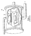
- FIG. 1 A schematic representation of a typical HFCVD reactor used in prior art diamond growth processes is shown in Figure 1.
- the reactor 10 comprises a chamber 12 enclosing a resistively heated filament 14 and a heated or cooled substrate holder 16 on which a substrate 17 is placed. Pumps and pressuring monitoring equipment is included (not shown).
- the reactant gas mixture is fed into the chamber through a gas diffuser unit 18.
- the filament 14 is made from a high melting-point refractory metal, such as tungsten or tantalum, and is heated to between 1800 - 2300°C to dissociate hydrogen and other molecules in the reactant gas mixture which normally contains a mixture of hydrogen and hydrocarbon. Atomic hydrogen and other dissociated products subsequently react with the reactant gas mixture to generate precursors responsible for diamond formation.
- the precursors then diffuse to and condense on substrate 17 for the formation of polycrystalline diamond.
- the separation between the filament and the substrate is normally in the range of 0.5 to 5 cm.
- the temperature of the substrate is generally maintained in the range of 700 to 1000°C.
- the deposition rate and reaction efficiency are determined by a combination of the rate of reactant generation near the filaments, the rate of reactant diffusion to the substrate, and the probability of diamond formation on the substrate.
- Figure 2 illustrates several modifications of the conventional HFCVD by coupling the process with direct current (DC) plasma CVD as proposed by A. Ikegaya and T. Masaaki in JP 173366 (1986), JP 75282 (1987), and European Patent 0254312 A1.
- a hot filament 20 is used as a thermionic electron emitter and a grid electrode 22 is inserted between the hot filament 20 and the substrate 24.
- the filament 20 and the substrate 24 are both negatively biased against the grid electrode 22 using power supplies 26 in order to form a DC plasma between the filament 20 and grid 22, and the grid 22 and substrate 24.
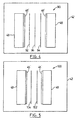
- FIG. 3 is a schematic diagram of an apparatus 40 for implementing the method of nucleating and growing diamond in accordance with the present invention.
- the reactant gas mixture is introduced into a deposition chamber 42 through a gas shower unit 44.
- the substrate 46 on which the diamond film is being deposited is placed on a substrate holder 48 which may be heated or cooled by a heat exchange fluid running through conduits 50.
- the substrate holder 48 is equipped with a thermocouple 52 for sensing the temperature of the substrate holder and may be connected to a substrate temperature controller 54 that controls the temperature of the heat exchange fluid.
- a filament array 58 is mounted on conducting rods 60 and is spaced above substrate holder 48.
- a grid electrode 64 is mounted on conducting rods 66 and is spaced above filament array 58 so that a sequential grid-filament-substrate assembly is provided.
- the filament array 58 is preferably spaced less than 2 cm from the top of substrate 46.
- the grid electrode 64 is preferably spaced less than 5 cm from filament array 58.
- Grid electrode 64 is shown as a wire grid in Figure 3 but may also be constructed from a wire mesh, metal rods or a perforated metal plate able to withstand the operating temperatures.
- Filament array 58 is comprised of a plurality of conductive metal filaments with a high melting point such as Ta and W. Filament array 58 can withstand resistive heating to temperatures above 2000°C, the preferred temperature range for dissociating hydrogen in the reactant gas. Grid electrode 64 and filament array 58 are shown as being substantially parallel in chamber 42 but it will be appreciated that these components do not need to be parallel to each other.
- DC power supplies 72 and 74 are used to provide the DC bias requirements during substrate nucleation and diamond coating growth. More specifically, power supply 74 is used to maintain the bias requirements between the filament array 58 and substrate 46 and power supply 72 provides the bias requirements between the grid electrode 64 and filament array 58. It will be understood that the substrate on which the diamond film is being deposited is typically electrically conductive so the substrate will be biased to the same potential as the substrate holder.
- the filament array 58 is maintained in the temperature range of 1800-2600°C using a power supply 78 which is preferably an AC power supply.
- the power density is about 20-500 W/cm 2 .
- the plasma power density during growth is about 1-300W/cm 2 .
- the grid electrode 64 may be either heated or cooled during deposition of the diamond film.
- the grid electrode 64 may be heated resistively and/or by plasma energy.
- Grid 64 may comprise hollow rods and may be cooled by running a heat exchange fluid through the centre of the electrode rods.
- the temperature of filament array 58 and grid electrode 64 is monitored by an optical pyrometer (not shown) which is located outside the deposition chamber 42 and focussed onto filament array 58 through a window 70 in the vacuum chamber.
- the gas flow and pressure are controlled by conventional flow meters and controllers, vacuum pumps and gauges (not shown).
- the reactant gas mixture comprises hydrogen, at least one carbon source including hydrocarbons, hydrocarbons containing oxygen and/or nitrogen, hydrocarbons containing halogens, carbon vapor, CO, CO 2 , and optionally other gases such as O 2 , F 2 , and H 2 O.
- the reactant gas pressure is set in the range between 10 to 500 Torr.
- the power density is about 20-500 W/cm 2 .
- the plasma power density during growth is about 1-300W/cm 2 .
- the growth substrate 46 is maintained at ground potential for both the step of nucleation and diamond growth.
- the power density for resistively heating the filament array 58 is about 20-500 W/cm 2 .
- the filament array 58 is biased positively with respect to the substrate, preferably in the range of 20-300 Volts positive with respect to the substrate. It will be understood that maintaining the substrate at ground potential is preferred but it could be maintained at potentials in the vicinity of ground so long as the filament array 58 is at a more positive potential than the substrate holder.
- the grid electrode 64 is biased positively with respect to the filament array, preferably in the range of 20-300 Volts with respect to the filament array 58 so that during nucleation the grid electrode 64 is maintained at a voltage more positive than the filament array. Therefore, during diamond nucleation, a plasma is maintained between the filament electrode 58 and grid 64 and thermionic emission from the heated filament array 58 enhances the plasma density. Ions in the DC plasma are extracted towards the substrate 46 for particle bombardment assisted nucleation.
- the nucleation process according to the method disclosed herein advantageously takes less than ten minutes.
- the unique configuration of the present invention allows the maintenance of the substrate 46 at potentials more negative than the heated filament array 58 thereby resulting in ion extraction towards the substrate 46 to achieve enhanced diamond nucleation.
- the filament array 58 is either electrically connected to the substrate holder 48, or alternatively it may be biased negative with respect to the substrate holder 48, preferably in the range of -20 to -300 Volts.
- Grid electrode 64 is biased positive with respect to the filament array 58, and preferably in the range 20-300 Volts with respect to the filament array 58 whether or not the filament array is held at ground.
- the typical plasma energy density is about 1-300 W/cm 2 .
- the large cathode voltage drop near the filament array 58 will extract some ions from the plasma towards the filaments. Due to the small mean free path for collision at the processing pressure (about 0.01 mm at 50 Torr and 1500K), such an ion extraction in the direction towards the substrate 46 will result in the partitioning of the ion energy into kinetic energy for neutrals in the collision cascades. In turn, these accelerated neutrals will have a net average velocity towards the substrate 46 and an average energy higher than the average thermal energy in the system thereby resulting in an enhanced reaction probability. However, the average energy will be much less than a few electron volts, which is not sufficient for inducing any significant sputtering action on the substrate 46. The motion of neutrals towards the substrate 46 enhances the arrival rate of the growth precursors beyond that induced by simple diffusion, thereby enhancing the diamond growth rate.
- a DC plasma can also be maintained between the filament array 58 and substrate 46.
- a high DC power input in this operation mode may lead to an increase in temperature of the substrate surface outside the diamond growth window, which is a limitation common to other prior art hot filament DC plasma growth techniques. Accordingly, under the normal operation in the present invention, the plasma power input between the grid electrode 64 and filament array 58 is higher than that between the filament array and substrate 46.
- Figure 4 shows a substrate-hot filament-grid-hot filament-substrate configuration at 90 for depositing diamond coatings onto two substrates 46' affixed to the opposed substrate holders 48.
- the array 90 may be assembled in vacuum chamber 42 vertically as shown or alternatively the entire assembly may be rotated 90° to a horizontal position within the chamber.
- the two hot filament arrays 92 and 94 may be heated either by independent DC or AC power supplies, or by a shared DC or AC power supply (not shown).
- Each of the two filament arrays 92 and 94 are provided with a DC power supply for biasing the arrays with respect to ground (not shown).
- a grid electrode 96 is located between filament arrays 92 and 94 and is biased using a DC power supply (not shown) and is biased at a positive potential relative to the filament arrays 92 and 94, preferably in range from 20-300 Volts.
- the filament arrays 92 and 94 are biased at a positive potential relative to the associated substrates 46' adjacent thereto.
- the filament arrays 92 and 94 are either not biased at all or biased negatively with respect the associated substrates 46', similar to the process described above with respect to the apparatus of Figure 3.
- the operation range is the same as those discussed in relation to Figure 3.
- Figure 5 shows another configuration 100 for growing diamond coatings according to the present invention.
- Two filament arrays 102 and 104 are resistively heated by independent AC or DC power supplies (not shown). Both groups of hot filament arrays 102 and 104 serve the function of grid electrodes so that in operation the two filament arrays are biased appropriately to maintain the plasma discharge between the two filament arrays using either an AC or DC power supply, preferably an AC power supply (not shown).
- Diamond nucleation even on mirror-smooth quartz was achieved by biasing filament array 58 at 89 Volts and heated to a temperature of about 2160°C and biasing grid 64 at 200 Volts using the apparatus of Figure 3.
- the reactant gas mixture was a mixture of methane/H 2 and respective flow rates were 6.5 standard cubic centimetres per minute (sccm) for methane and 300 sccm for hydrogen at a total pressure of 30 Torr.
- the nucleation process was maintained for about 10 minutes.
- the bias on filament array 58 was then switched off and the bias on grid electrode 64 was adjusted to 120 Volts for diamond growth. A coherent and uniform well faceted diamond film was obtained. Under the same growth conditions but without the nucleation step, only patches of diamond with non-uniform thickness were formed on mirror-smooth quartz. Subsequent runs showed that the nucleation time could be in the range of 2-5 minutes.
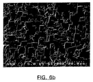
- Diamond oriented crystals were grown on silicon (100) by precleaning the silicon with an HF solution, and nucleating with a filament temperature of about 2200°C, a grid bias of 219 Volts, and a filament bias of 130 Volts using the method and apparatus of Figure 3.
- the reactant gas mixture was a mixture of methane/H 2 and respective flow rates were 6 sccm for methane and 300 sccm for hydrogen at a total pressure of 50 Torr.
- the nucleation time was about 10 minutes.
- the filament array was then biased to zero volts for diamond growth.
- the grid bias was changed to 112 Volts in this process.
- Figure 6a clearly shows diamond (100) cubic crystals with its (100) face aligned with the Si (100), and the diamond direction [110] aligned with that of Si [110].
- diamond was grown with a high nucleation density, a coherent film with diamond (100)//Si(100), and diamond [110]//Si[110] was formed, as that shown in Figure 6b.
- a diamond coating was grown for 160 hours to 2.5 mm in thickness and 2" in diameter using the apparatus of Figure 3.
- the pressure for diamond growth was 30 Torr and bias voltage on the grid electrode was 45 Volts relative to the filament array.
- the filament power density was about 170 W/cm 2 and the plasma power density was 40W/cm 2 .
- the growth rate was 16 ⁇ m/hr. Both Raman and X-ray photoelectron spectroscopy showed pure diamond and no impurities in the sample (data not shown).
- a diamond coating was grown for 44 hours to 0.93 mm in thickness and 2" in diameter on a substrate using the apparatus of Figure 3.
- the pressure for diamond growth was 30 Torr and bias voltage on the grid electrode was 50 Volts relative to the filament array.
- the growth rate was 21 ⁇ m/hr.
- Both Raman and X-ray photoelectron spectroscopy showed pure diamond and no impurities in the sample (data not shown).
- the filament power density was about 170W/cm 2 and the plasma power density was about 50W/cm 2 .
- the present method is advantageous over the diamond film growth process disclosed in EP0254560 because in the latter an ion extraction assisted diamond nucleation step cannot be performed due to the fact that the hot filaments are effective electron emitters, and thus most effectively used as a cathode in a DC plasma configuration.
- the substrate can only be used effectively as an anode, and ions in the plasma are attracted to the cathode instead of anode.
- the present method is advantageous over the diamond film growth process disclosed in EP0254312 because the grid electrode in EP0254312 is located between the filaments and substrate, and is always biased positively to the filaments to maintain a DC plasma.
- the ion extraction from the plasma between the grid and filaments towards the cathode hot filaments will induce a net flow of neutrals in the ion-neutral collision cascades away from the substrate.
- many growth reactants generated on and near the hot filaments, and those generated in the plasma are not advantageously utilized and therefore wasted.
- the substrate is biased negatively to the grid, some ions from the plasma can be extracted towards the substrate, these ions are extracted from the anode (the grid) of the DC plasma between the filaments and the grid. Hence, the extraction is not efficient, as compared to the technology disclosed in the present application.
- the typical distance between the filament and the top of the substrate being coated in a hot filament CVD system is about 0.5-1 cm. Hence, the insertion of a grid into this space for uniform deposition is technically difficult. Any increase of the filament-substrate separation will decrease the efficiency of hot filament diamond CVD.
- the diamond growth process described in WO92/01828 teaches a filament rack of resistively heated filaments located between two growth substrates such that a DC discharge can be ignited between the filaments and substrates.
- a DC discharge can be ignited between the filaments and substrates.
- Such an arrangement is very similar to the technology described in EP254560.
- the main difference between this approach and the technology disclosed herein is the lack of flexibility in this approach and its inability to process ion extraction and particle bombardment induced diamond nucleation and growth.
- the DC plasma current is directly drawn from the substrate.
- the problem is that the maximum power density is limited by the substrate temperature which cannot be higher than the diamond growth temperature range.
- the DC plasma can be maintained outside the filament-substrate region such that the total energy density directly deposited on the substrate surface will not be exceedingly high and yet activated reactants can still be yielded and transported to the substrate.
- the new diamond growth process disclosed herein provides an enhanced nucleation density and growth rate due to the addition of DC plasmas to the hot filament CVD of diamond with electrode configuration (substrate-hot filament-grid) which allows efficient ion extraction and growth precursor transportation towards the substrate during diamond nucleation and growth respectively as compared to the filament-grid-substrate configuration, and substrate-filament-substrate configuration.
- the present method provides considerable flexibility in maintaining the DC plasma away from the substrate surface for the minimization of excessive substrate heating.
Landscapes
- Chemical & Material Sciences (AREA)
- Engineering & Computer Science (AREA)
- Materials Engineering (AREA)
- Metallurgy (AREA)
- Organic Chemistry (AREA)
- Chemical Kinetics & Catalysis (AREA)
- General Chemical & Material Sciences (AREA)
- Mechanical Engineering (AREA)
- Plasma & Fusion (AREA)
- Physics & Mathematics (AREA)
- Inorganic Chemistry (AREA)
- Crystallography & Structural Chemistry (AREA)
- Analytical Chemistry (AREA)
- Combustion & Propulsion (AREA)
- Health & Medical Sciences (AREA)
- Toxicology (AREA)
- Crystals, And After-Treatments Of Crystals (AREA)
- Chemical Vapour Deposition (AREA)
Claims (17)
- Verfahren zum Aufwachsen eines Diamantfilms durch Heizfadenentladung, umfassend:a) Positionieren eines Substrats, das eine Aufdampfoberfläche aufweist, auf einer Substrathalterung in einer Aufdampfkammer; Bereitstellen einer Gitterelektrode, die mit Zwischenraum von der Substrataufdampfoberfläche angeordnet ist; Bereitstellen einer Heizfadenfeldelektrode, die zwischen der Gitterelektrode und der Substrataufdampfoberfläche zwischengeschaltet ist;b) Strömen eines Gasgemisches, das aus Wasserstoff und kohlenstoffhaltigem Gas besteht, in die Aufdampfkammer und Widerstandsheizen der Heizfadenfeldelektrode auf eine Temperatur im Bereich von 1.800 °C bis 2.600 °C, wobei das Substrat auf eine Temperatur im Bereich von 600 °C bis 1.100 °C erhitzt wird;c) Keimbildung des Substrats durch Vorspannung der Heizfadenfeldelektrode bei einer positiven Spannung bezüglich der Substrathalterung und Vorspannung der Gitterelektrode bei einer Spannung, die bezüglich der Spannung an der Heizfadenfeldelektrode positiv ist; danachd) Vorspannung der Gitterelektrode bei einer Spannung, die bezüglich der Spannung an der Heizfadenfeldelektrode positiv ist, um einen Diamantfilm auf der Aufdampfoberfläche aufzudampfen.
- Verfahren nach Anspruch 1, wobei das Substrat während der Keimbildung des Substrats bei Erdpotential vorgespannt wird und die Heizfadenfeldelektrode auf ein Potential im Bereich von 20 bis 300 Volt bezüglich Erde vorgespannt wird, und die Gitterelektrode auf eine Spannung im Bereich von 20 bis 300 Volt bezüglich der Heizfadenfeldelektrode vorgespannt wird.
- Verfahren nach Anspruch 2, wobei während des Schrittes des Aufwachsens des Diamantfilms nach dem Schritt der Keimbildung die Substrathalterung und die Heizfadenfeldelektrode bei Erdpotential vorgespannt werden und die Gitterelektrode bei einer Spannung im Bereich von 20 bis 300 Volt bezüglich der Heizfadenfeldelektrode vorgespannt wird.
- Verfahren nach Anspruch 2, wobei während des Schrittes des Aufwachsens des Diamantfilms nach dem Schritt der Keimbildung die Substrathalterung bei Erdpotential vorgespannt wird und die Heizfadenfeldelektrode bei einer negativen Spannung bezüglich der Substrathalterung vorgespannt wird, wobei die negative Spannung in einem Bereich von -20 bis -300 Volt bezüglich der Substrathalterung liegt.
- Verfahren nach Anspruch 1, wobei das kohlenstoffhaltige Gas aus der Gruppe ausgewählt wird, die aus Kohlenwasserstoffen, sauerstoff- und/oder stickstoffhaltigen Kohlenwasserstoffen, halogenhaltigen Kohlenwasserstoffen, Kohlenstoffdampf, CO und CO2 besteht.
- Verfahren nach Anspruch 5, wobei das Gasgemisch ferner eines von O2, F2 und H2O und ein Inertgas und jede Kombination davon enthält.
- Verfahren nach Anspruch 5, wobei das Gasgemisch bei einem Druck im Bereich von 10 bis 500 Torr gehalten wird.
- Verfahren nach Anspruch 1, wobei die Heizfadenfeldelektrode unter Verwendung einer Stromversorgung widerstandsbeheizt wird, die aus einer Gruppe ausgewählt ist, die aus Wechselstrom- und Gleichstromstromversorgungen besteht.
- Plasmavorrichtung mit Heizfaden-Gleichstromentladung für das Synthetisieren eines Diamantfilms, umfassend:a) eine Aufdampfkammer (42), die einen Gaseintritt für das Strömen der Reaktionsgase in die Aufdampfkammer (42) aufweist;b) eine erste und eine zweite mit Zwischenraum angeordnete leitende Substrathalterung (48), wobei jede geeignet ist, ein Substrat (46') zu tragen, das eine Oberfläche, auf welcher der Diamantfilm synthetisiert werden soll, und Mittel für das Heizen und das Kühlen der ersten und der zweiten Substrathalterung (48) aufweist;c) eine Gitterelektrode (96), die zwischen der ersten und der zweiten Substrathalterung (48) angeordnet ist;d) eine erste Heizfadenfeldelektrode (92), die zwischen der ersten Substrathalterung (48) und der Gitterelektrode (96) zwischengeschaltet ist, und eine zweite Heizfadenfeldelektrode (94), die zwischen der zweiten Substrathalterung (48) und der Gitterelektrode (96) zwischengeschaltet ist, und Mittel für das Widerstandsheizen der ersten und der zweiten Heizfadenfeldelektrode (92, 94); unde) Mittel für das Vorspannen der Gitterelektrode (96) und der ersten und der zweiten Heizfadenfeldelektrode (92, 94) und der ersten und der zweiten Substrathalterung (48), um ein Plasma mit Heizfaden-Gleichstromentladung zu erzeugen, einschließlich Mittel für das Einstellen des Vorspannungspotentials an der Gitterelektrode (96) und der ersten und der zweiten Heizfadenfeldelektrode (92, 94) bezüglich einander und der ersten und der zweiten Substrathalterung (48).
- Vorrichtung nach Anspruch 9, wobei die Substrate auf der ersten und der zweiten Substrathalterung angeordnet sind, wobei die erste Heizfadenfeldelektrode mit Zwischenraum von der Oberfläche des ersten Substrats angeordnet ist, auf welchem der Diamantfilm in einem Abstand von kleiner oder gleich 2 cm synthetisiert wird, wobei die erste Heizfadenfeldelektrode mit Zwischenraum von der Gitterelektrode in einem Abstand kleiner oder gleich 5 cm angeordnet wird, und wobei die zweite Heizfadenfeldelektrode mit Zwischenraum von der Oberfläche des zweiten Substrats angeordnet ist, auf welchem der Diamantfilm in einem Abstand kleiner oder gleich 2 cm synthetisiert wird, wobei die zweite Heizfadenfeldelektrode mit Zwischenraum von der Gitterelektrode in einem Abstand kleiner oder gleich 5 cm angeordnet wird.
- Vorrichtung nach Anspruch 9, wobei die Mittel für das Widerstandsheizen der ersten und der zweiten Heizfadenfeldelektrode aus der Gruppe ausgewählt sind, die aus Wechselstrom- und Gleichstromstromversorgungen besteht.
- Vorrichtung nach Anspruch 9, wobei die Mittel für das Heizen und das Kühlen der ersten und der zweiten Substrathalterung ein Thermoelement enthalten, das an jeder Substrathalterung angebracht und an einen Temperaturregler angeschlossen ist.
- Vorrichtung nach Anspruch 9, wobei die Gitterelektrode aus der Gruppe ausgewählt ist, die aus mit Zwischenraum angeordneten Stäben, Drahtfeldern, Drahtgeflecht und einer Metallplatte mit mehreren Bohrungen darin besteht.
- Vorrichtung nach Anspruch 13, die ferner Heiz- und Kühlmittel für das Heizen und das Kühlen der Gitterelektrode enthält.
- Verfahren zum Aufwachsen eines Diamantfilms durch Heizfadenentladung, umfassend:a) Positionieren der Substrate (46'), wobei jedes eine Aufdampfoberfläche auf der ersten und der zweiten mit Zwischenraum angeordneten Substrathalterung (48) in einer Aufdampfkammer (42) aufweist, Bereitstellen einer Gitterelektrode (96), die zwischen der ersten und der zweiten Substrathalterung (48) angeordnet ist, und einer ersten Heizfadenfeldelektrode (92), die zwischen der ersten Substrathalterung (48) und der Gitterelektrode (96) zwischengeschaltet ist, und einer zweiten Heizfadenfeldelektrode (94), die zwischen der zweiten Substrathalterung (48) und der Gitterelektrode (96) zwischengeschaltet ist;b) Strömen eines Gasgemisches, das aus Wasserstoff und kohlenstoffhaltigem Gas besteht, in die Aufdampfkammer (42) und Widerstandsheizen der ersten und der zweiten Heizfadenfeldelektrode (92, 94) auf eine Temperatur im Bereich von 1.800 °C bis 2.600 °C, wobei die Substrate (46') auf eine Temperatur im Bereich von 600 °C bis 1.100 °C erhitzt werden;c) Keimbildung der Substrate (46') auf der ersten und der zweiten Substrathalterung (48) durch Vorspannung der ersten Heizfadenfeldelektrode (92) bei einer positiven Spannung bezüglich der ersten Substrathalterung (48), um ein Plasma bereitzustellen, das einen effektiven Potentialabfall zwischen der Gitterelektrode (96) und dem ersten Substrat (46') für die effiziente Ionenextraktion im Plasma zu den Substraten (46') auf der zweiten Substrathalterung (48) aufweist; danachd) Vorspannung der Gitterelektrode (96) bei einer Spannung, die bezüglich der Spannung an der ersten und der zweiten Heizfadenfeldelektrode (92, 94) positiv ist, um einen Diamantfilm auf den Aufdampfoberflächen der Substrate (46') auf der ersten und der zweiten Substrathalterung (48) aufzudampfen.
- Verfahren nach Anspruch 15, wobei die Substrate auf Substrathalterungen angeordnet sind, wobei die erste Heizfadenfeldelektrode mit Zwischenraum von der Aufdampfoberfläche der Substrate auf der ersten Substrathalterung in einem Abstand kleiner oder gleich 2 cm angeordnet ist, wobei die erste Heizfadenfeldelektrode mit Zwischenraum von der Gitterelektrode in einem Abstand kleiner oder gleich 5 cm angeordnet wird, und wobei die zweite Heizfadenfeldelektrode mit Zwischenraum von der Aufdampfoberfläche der Substrate auf der zweiten Substrathalterung in einem Abstand kleiner oder gleich 2 cm angeordnet ist, wobei die zweite Heizfadenfeldelektrode mit Zwischenraum von der Gitterelektrode in einem Abstand kleiner oder gleich 5 cm angeordnet wird.
- Verfahren nach Anspruch 15, wobei die erste und die zweite Heizfadenfeldelektrode unter Verwendung einer Stromversorgung widerstandsbeheizt sind, die aus einer Gruppe ausgewählt ist, die aus Wechselstrom- und Gleichstromstromversorgungen besteht.
Applications Claiming Priority (3)
| Application Number | Priority Date | Filing Date | Title |
|---|---|---|---|
| US08/888,830 US6161499A (en) | 1997-07-07 | 1997-07-07 | Apparatus and method for nucleation and deposition of diamond using hot-filament DC plasma |
| US888830 | 1997-07-07 | ||
| PCT/CA1998/000645 WO1999002753A1 (en) | 1997-07-07 | 1998-07-07 | Apparatus and method for nucleation and deposition of diamond using hot-filament dc plasma |
Publications (2)
| Publication Number | Publication Date |
|---|---|
| EP0994973A1 EP0994973A1 (de) | 2000-04-26 |
| EP0994973B1 true EP0994973B1 (de) | 2003-06-04 |
Family
ID=25393993
Family Applications (1)
| Application Number | Title | Priority Date | Filing Date |
|---|---|---|---|
| EP98931851A Expired - Lifetime EP0994973B1 (de) | 1997-07-07 | 1998-07-07 | Vorrichtung und verfahren zur keimbildung und abscheidung von diamant mittels heissdraht-dc-plasma |
Country Status (10)
| Country | Link |
|---|---|
| US (2) | US6161499A (de) |
| EP (1) | EP0994973B1 (de) |
| JP (1) | JP2002506786A (de) |
| KR (1) | KR20010021551A (de) |
| CN (1) | CN1125890C (de) |
| AU (1) | AU8201798A (de) |
| BR (1) | BR9810576A (de) |
| CA (1) | CA2294715C (de) |
| DE (1) | DE69815348T2 (de) |
| WO (1) | WO1999002753A1 (de) |
Families Citing this family (59)
| Publication number | Priority date | Publication date | Assignee | Title |
|---|---|---|---|---|
| TW455912B (en) | 1999-01-22 | 2001-09-21 | Sony Corp | Method and apparatus for film deposition |
| DE19911746A1 (de) * | 1999-03-16 | 2000-09-21 | Basf Ag | Diamantelektroden |
| US6692574B1 (en) * | 1999-08-30 | 2004-02-17 | Si Diamond Technology, Inc. | Gas dispersion apparatus for use in a hot filament chemical vapor deposition chamber |
| US6582780B1 (en) * | 1999-08-30 | 2003-06-24 | Si Diamond Technology, Inc. | Substrate support for use in a hot filament chemical vapor deposition chamber |
| US6432206B1 (en) * | 1999-08-30 | 2002-08-13 | Si Diamond Technology, Inc. | Heating element for use in a hot filament chemical vapor deposition chamber |
| RU2194329C2 (ru) * | 2000-02-25 | 2002-12-10 | ООО "Высокие технологии" | Способ получения адресуемого автоэмиссионного катода и дисплейной структуры на его основе |
| KR100458779B1 (ko) * | 2000-03-27 | 2004-12-03 | 미츠비시 쥬고교 가부시키가이샤 | 금속막의 제작방법 및 그 제작장치 |
| US6638839B2 (en) * | 2001-07-26 | 2003-10-28 | The University Of Toledo | Hot-filament chemical vapor deposition chamber and process with multiple gas inlets |
| KR20030028296A (ko) * | 2001-09-28 | 2003-04-08 | 학교법인 한양학원 | 플라즈마 화학기상증착 장치 및 이를 이용한 탄소나노튜브제조방법 |
| JP3840147B2 (ja) * | 2002-06-21 | 2006-11-01 | キヤノン株式会社 | 成膜装置、成膜方法およびそれを用いた電子放出素子、電子源、画像形成装置の製造方法 |
| KR100466406B1 (ko) * | 2002-07-08 | 2005-01-13 | 한국과학기술연구원 | 미세, 정밀, 건식 가공이 가능한 다이아몬드 막이 증착된절삭공구 및 이의 제조방법 |
| EP1429224A1 (de) * | 2002-12-10 | 2004-06-16 | Texas Instruments Incorporated | Firmware Laufzeit Authentisierung |
| AT412653B (de) * | 2003-06-26 | 2005-05-25 | Physikalisches Buero Steinmuel | Verfahren zur anbringung eines identifizierungsmerkmals |
| AT500171B8 (de) * | 2003-09-10 | 2007-02-15 | Physikalisches Buero Steinmuel | Verfahren zur herstellung eines diamantbeschichteten bauteils |
| WO2005031781A1 (ja) * | 2003-09-30 | 2005-04-07 | Sumitomo Electric Industries, Ltd. | ダイヤモンド電子放出素子の製造方法ならびに電子放出素子 |
| JP4691377B2 (ja) * | 2005-03-28 | 2011-06-01 | 株式会社アルバック | 薄膜形成方法 |
| JP4736564B2 (ja) | 2005-06-23 | 2011-07-27 | 東京エレクトロン株式会社 | 載置台装置の取付構造及び処理装置 |
| CN1925696B (zh) * | 2005-09-01 | 2010-10-13 | 中国砂轮企业股份有限公司 | 钻石振动膜 |
| US7521341B2 (en) * | 2005-11-09 | 2009-04-21 | Industrial Technology Research Institute | Method of direct deposition of polycrystalline silicon |
| PT1962873E (pt) * | 2005-12-14 | 2013-08-29 | Oxthera Inc | Composições farmacêuticas compreendendo bactérias redutoras de oxalato |
| ES2362897T3 (es) * | 2005-12-16 | 2011-07-14 | Oxthera, Inc. | Composiciones y métodos para reducción del oxalato. |
| ITMI20070056A1 (it) * | 2007-01-17 | 2008-07-18 | Consiglio Nazionale Ricerche | Substrato semiconduttore adatto alla realizzazione di dispositivi elettronici e-o optoelettronici e relativo processo di fabbricazione |
| US20080241413A1 (en) * | 2007-03-26 | 2008-10-02 | Ravi Kramadhati V | Plasma tool for forming porous diamond films for semiconductor applications |
| KR100924287B1 (ko) * | 2007-05-10 | 2009-10-30 | 한국과학기술연구원 | 양광주가 존재하지 않는 직류 전원 플라스마 증착 장치와,양광주를 배제한 상태에서의 물질 증착 방법 및 이에 의해제조된 다이아몬드 박막 |
| US8251876B2 (en) | 2008-04-22 | 2012-08-28 | Hill-Rom Services, Inc. | Breathing exercise apparatus |
| US20110070370A1 (en) * | 2008-05-28 | 2011-03-24 | Aixtron Ag | Thermal gradient enhanced chemical vapour deposition (tge-cvd) |
| JP2012504873A (ja) * | 2008-10-03 | 2012-02-23 | ビーコ プロセス イクイップメント, インコーポレイテッド | 気相エピタキシーシステム |
| WO2011106624A1 (en) * | 2010-02-26 | 2011-09-01 | Alliance For Sustainable Energy, Llc | Hot wire chemical vapor deposition (hwcvd) with carbide filaments |
| US20110244128A1 (en) * | 2010-03-31 | 2011-10-06 | Tokyo Electron Limited | Flow plate utilization in filament assisted chemical vapor deposition |
| BE1019439A3 (fr) * | 2010-07-30 | 2012-07-03 | Diarotech | Procede pour synthetiser par depot chimique en phase vapeur une matiere solide, en particulier du diamant, ainsi qu'un dispositif pour l'application du procede. |
| US8895115B2 (en) * | 2010-11-09 | 2014-11-25 | Southwest Research Institute | Method for producing an ionized vapor deposition coating |
| WO2012161561A1 (en) | 2011-05-24 | 2012-11-29 | Mimos Berhad | Method and apparatus for depositing nanomaterials |
| CN102251231A (zh) * | 2011-07-29 | 2011-11-23 | 广州市德百顺电气科技有限公司 | 一种纳米金刚石薄膜的制备方法 |
| CN102290260B (zh) * | 2011-07-29 | 2014-02-26 | 广州市德百顺电气科技有限公司 | 一种电触头及其制备方法 |
| EP2820173B1 (de) * | 2012-02-29 | 2022-08-24 | RFHIC Corporation | Substrat für galliumnitrid-auf-diamant wafer abscheidung |
| US9180271B2 (en) | 2012-03-05 | 2015-11-10 | Hill-Rom Services Pte. Ltd. | Respiratory therapy device having standard and oscillatory PEP with nebulizer |
| CN102719804B (zh) * | 2012-07-02 | 2014-12-10 | 兰州大学 | 气体内循环型热丝cvd金刚石膜生长装置 |
| KR101252669B1 (ko) * | 2012-07-02 | 2013-04-09 | 한국과학기술연구원 | 다이아몬드 고속성장방법 및 장치 |
| JP5842761B2 (ja) * | 2012-08-07 | 2016-01-13 | 信越化学工業株式会社 | ダイヤモンドの製造方法及び直流プラズマcvd装置 |
| CN103215561B (zh) * | 2013-04-24 | 2015-11-18 | 中国科学院物理研究所 | 一种等离子体沉积及刻蚀系统 |
| DE102013112855A1 (de) | 2013-11-21 | 2015-05-21 | Aixtron Se | Vorrichtung und Verfahren zum Fertigen von aus Kohlenstoff bestehenden Nanostrukturen |
| CN105506575A (zh) * | 2015-12-08 | 2016-04-20 | 中国电子科技集团公司第十二研究所 | 一种低温纳米/超纳米金刚石薄膜的制造设备和方法 |
| AT519217B1 (de) * | 2016-10-04 | 2018-08-15 | Carboncompetence Gmbh | Vorrichtung und Verfahren zum Aufbringen einer Kohlenstoffschicht |
| CN106756890B (zh) * | 2016-11-24 | 2019-07-23 | 郑州航空工业管理学院 | 一种化学气相沉积用的反应装置 |
| US20180308667A1 (en) * | 2017-04-24 | 2018-10-25 | Kenneth S. Collins | Plasma reactor with groups of electrodes |
| TWI800505B (zh) * | 2017-04-24 | 2023-05-01 | 美商應用材料股份有限公司 | 對電漿反應器的電極施加功率 |
| US11424104B2 (en) * | 2017-04-24 | 2022-08-23 | Applied Materials, Inc. | Plasma reactor with electrode filaments extending from ceiling |
| US10510515B2 (en) | 2017-06-22 | 2019-12-17 | Applied Materials, Inc. | Processing tool with electrically switched electrode assembly |
| US11355321B2 (en) * | 2017-06-22 | 2022-06-07 | Applied Materials, Inc. | Plasma reactor with electrode assembly for moving substrate |
| TWI794240B (zh) * | 2017-06-22 | 2023-03-01 | 美商應用材料股份有限公司 | 用於電漿處理的處理工具及電漿反應器 |
| WO2019003151A1 (en) * | 2017-06-28 | 2019-01-03 | Icdat Ltd. | SYSTEM AND METHOD FOR CHEMICAL VAPOR DEPOSITION OF SYNTHETIC DIAMONDS |
| KR101966794B1 (ko) * | 2017-07-12 | 2019-08-27 | (주)선재하이테크 | 전자 집속 개선용 엑스선관 |
| EP3669014B1 (de) * | 2017-08-18 | 2024-08-07 | Gühring KG | Verfahren zum beschichten temperaturempfindlicher substrate mit polykristallinem diamant |
| CN108396308B (zh) * | 2018-05-03 | 2023-06-09 | 广东鼎泰高科精工科技有限公司 | 一种具有多个热丝装置的cvd金刚石涂层设备 |
| JP7061049B2 (ja) * | 2018-09-10 | 2022-04-27 | 株式会社神戸製鋼所 | 熱フィラメントcvd装置 |
| CN110306151A (zh) * | 2019-07-22 | 2019-10-08 | 上海妙壳新材料科技有限公司 | 一种高速钢自润滑涂层前处理设备及其使用方法 |
| AU2021225841A1 (en) * | 2020-02-24 | 2022-09-15 | Advanced Diamond Holdings, Llc | Plasma shaping for diamond growth |
| CN113026001B8 (zh) * | 2021-05-26 | 2021-09-14 | 上海征世科技股份有限公司 | 一种介稳态控制制备金刚石的方法 |
| CN115466939A (zh) * | 2022-10-10 | 2022-12-13 | 中国科学院上海微系统与信息技术研究所 | 一种光调制化学气相沉积装置以及利用其调制薄膜生长温度的方法 |
Family Cites Families (17)
| Publication number | Priority date | Publication date | Assignee | Title |
|---|---|---|---|---|
| JPS6065796A (ja) | 1983-09-20 | 1985-04-15 | Nippon Telegr & Teleph Corp <Ntt> | 硬質カ−ボン膜及びその製造方法 |
| US4900628A (en) * | 1986-07-23 | 1990-02-13 | Sumitomo Electric Industries, Ltd. | Gaseous phase synthesized diamond and method for synthesizing same |
| JPH0649635B2 (ja) | 1986-07-23 | 1994-06-29 | 住友電気工業株式会社 | ダイヤモンドの合成方法 |
| US4859490A (en) * | 1986-07-23 | 1989-08-22 | Sumitomo Electric Industries, Ltd. | Method for synthesizing diamond |
| JP2501589B2 (ja) | 1986-07-23 | 1996-05-29 | 住友電気工業株式会社 | 気相合成ダイヤモンドおよびその合成方法 |
| US5185179A (en) * | 1988-10-11 | 1993-02-09 | Semiconductor Energy Laboratory Co., Ltd. | Plasma processing method and products thereof |
| JPH0780718B2 (ja) * | 1989-08-04 | 1995-08-30 | トヨタ自動車株式会社 | ダイヤモンドの合成方法および合成装置 |
| JPH03103397A (ja) | 1989-09-18 | 1991-04-30 | Sumitomo Electric Ind Ltd | 高強度ダイヤモンド |
| EP0521078B1 (de) * | 1990-03-20 | 1996-05-22 | Diamonex, Incorporated | Verbesserte glühfilament-cvd-anlage |
| US5314570A (en) * | 1990-07-18 | 1994-05-24 | Sumitomo Electric Industries Ltd. | Process and apparatus for the production of diamond |
| US5058527A (en) * | 1990-07-24 | 1991-10-22 | Ricoh Company, Ltd. | Thin film forming apparatus |
| US5145712A (en) * | 1991-02-08 | 1992-09-08 | Center For Innovative Technology | Chemical deposition of diamond |
| JP3103397B2 (ja) | 1991-08-27 | 2000-10-30 | キョーラク株式会社 | プログラムの不法使用防止システム |
| US5397428A (en) * | 1991-12-20 | 1995-03-14 | The University Of North Carolina At Chapel Hill | Nucleation enhancement for chemical vapor deposition of diamond |
| JPH05270982A (ja) | 1992-03-27 | 1993-10-19 | Idemitsu Petrochem Co Ltd | ダイヤモンド膜の製造方法 |
| US5698328A (en) | 1994-04-06 | 1997-12-16 | The Regents Of The University Of California | Diamond thin film electron emitter |
| JP3861346B2 (ja) * | 1996-12-04 | 2006-12-20 | 住友電気工業株式会社 | ダイヤモンド合成方法 |
-
1997
- 1997-07-07 US US08/888,830 patent/US6161499A/en not_active Expired - Fee Related
-
1998
- 1998-07-07 DE DE69815348T patent/DE69815348T2/de not_active Expired - Fee Related
- 1998-07-07 WO PCT/CA1998/000645 patent/WO1999002753A1/en not_active Ceased
- 1998-07-07 CN CN98806931A patent/CN1125890C/zh not_active Expired - Fee Related
- 1998-07-07 KR KR1020007000109A patent/KR20010021551A/ko not_active Abandoned
- 1998-07-07 AU AU82017/98A patent/AU8201798A/en not_active Abandoned
- 1998-07-07 JP JP2000502242A patent/JP2002506786A/ja active Pending
- 1998-07-07 CA CA002294715A patent/CA2294715C/en not_active Expired - Fee Related
- 1998-07-07 BR BR9810576-0A patent/BR9810576A/pt not_active Application Discontinuation
- 1998-07-07 EP EP98931851A patent/EP0994973B1/de not_active Expired - Lifetime
-
2000
- 2000-03-21 US US09/532,061 patent/US6200652B1/en not_active Expired - Fee Related
Also Published As
| Publication number | Publication date |
|---|---|
| JP2002506786A (ja) | 2002-03-05 |
| KR20010021551A (ko) | 2001-03-15 |
| EP0994973A1 (de) | 2000-04-26 |
| AU8201798A (en) | 1999-02-08 |
| US6200652B1 (en) | 2001-03-13 |
| CA2294715C (en) | 2007-05-22 |
| DE69815348T2 (de) | 2004-05-13 |
| CA2294715A1 (en) | 1999-01-21 |
| DE69815348D1 (de) | 2003-07-10 |
| US6161499A (en) | 2000-12-19 |
| WO1999002753A1 (en) | 1999-01-21 |
| BR9810576A (pt) | 2000-09-19 |
| CN1125890C (zh) | 2003-10-29 |
| CN1261927A (zh) | 2000-08-02 |
Similar Documents
| Publication | Publication Date | Title |
|---|---|---|
| EP0994973B1 (de) | Vorrichtung und verfahren zur keimbildung und abscheidung von diamant mittels heissdraht-dc-plasma | |
| US5368897A (en) | Method for arc discharge plasma vapor deposition of diamond | |
| US6110542A (en) | Method for forming a film | |
| US4740263A (en) | Process for preparing thin film and p-type diamond semiconductor | |
| US4434188A (en) | Method for synthesizing diamond | |
| US5039548A (en) | Plasma chemical vapor reaction method employing cyclotron resonance | |
| US4973494A (en) | Microwave enhanced CVD method for depositing a boron nitride and carbon | |
| US4830702A (en) | Hollow cathode plasma assisted apparatus and method of diamond synthesis | |
| EP0693573B1 (de) | Erzeugung eines Diamantfilmes | |
| US4898748A (en) | Method for enhancing chemical reactivity in thermal plasma processes | |
| US5993919A (en) | Method of synthesizing diamond | |
| EP0556615B1 (de) | Verfahren zur Herstellung von synthetischen Diamanten | |
| CN87107779A (zh) | 徽波增强式化学汽相淀积法及设备 | |
| US6677001B1 (en) | Microwave enhanced CVD method and apparatus | |
| MXPA00000295A (en) | Apparatus and method for nucleation and deposition of diamond using hot-filament dc plasma | |
| RU2788258C1 (ru) | Газоструйный способ осаждения алмазных пленок с активацией в плазме свч разряда | |
| Bachmann et al. | High rate versus low rate diamond CVD methods | |
| Bachmann et al. | Diamond forming discharges | |
| Olson et al. | Sequential Growth of High Quality Diamond Films from Hydrocarbon and Hydrogen Gases | |
| JPH0477709B2 (de) | ||
| KR20200065605A (ko) | 다음극 직류전원 플라즈마 cvd 다이아몬드 성장 장치 | |
| Beera | Synthesis and characterization of diamond and diamond-like carbon films for multichip modules | |
| JPH02157191A (ja) | 粒状ダイヤモンドの製造方法 | |
| JPH07166359A (ja) | プラズマ処理方法 | |
| JPH08203693A (ja) | 薄膜形成装置 |
Legal Events
| Date | Code | Title | Description |
|---|---|---|---|
| PUAI | Public reference made under article 153(3) epc to a published international application that has entered the european phase |
Free format text: ORIGINAL CODE: 0009012 |
|
| 17P | Request for examination filed |
Effective date: 20000204 |
|
| AK | Designated contracting states |
Kind code of ref document: A1 Designated state(s): BE DE ES FR GB IE IT SE |
|
| 17Q | First examination report despatched |
Effective date: 20000801 |
|
| GRAH | Despatch of communication of intention to grant a patent |
Free format text: ORIGINAL CODE: EPIDOS IGRA |
|
| GRAH | Despatch of communication of intention to grant a patent |
Free format text: ORIGINAL CODE: EPIDOS IGRA |
|
| GRAA | (expected) grant |
Free format text: ORIGINAL CODE: 0009210 |
|
| AK | Designated contracting states |
Designated state(s): BE DE ES FR GB IE IT SE |
|
| PG25 | Lapsed in a contracting state [announced via postgrant information from national office to epo] |
Ref country code: IT Free format text: LAPSE BECAUSE OF FAILURE TO SUBMIT A TRANSLATION OF THE DESCRIPTION OR TO PAY THE FEE WITHIN THE PRESCRIBED TIME-LIMIT;WARNING: LAPSES OF ITALIAN PATENTS WITH EFFECTIVE DATE BEFORE 2007 MAY HAVE OCCURRED AT ANY TIME BEFORE 2007. THE CORRECT EFFECTIVE DATE MAY BE DIFFERENT FROM THE ONE RECORDED. Effective date: 20030604 Ref country code: FR Free format text: LAPSE BECAUSE OF FAILURE TO SUBMIT A TRANSLATION OF THE DESCRIPTION OR TO PAY THE FEE WITHIN THE PRESCRIBED TIME-LIMIT Effective date: 20030604 Ref country code: BE Free format text: LAPSE BECAUSE OF FAILURE TO SUBMIT A TRANSLATION OF THE DESCRIPTION OR TO PAY THE FEE WITHIN THE PRESCRIBED TIME-LIMIT Effective date: 20030604 |
|
| REG | Reference to a national code |
Ref country code: GB Ref legal event code: FG4D |
|
| REG | Reference to a national code |
Ref country code: IE Ref legal event code: FG4D |
|
| REF | Corresponds to: |
Ref document number: 69815348 Country of ref document: DE Date of ref document: 20030710 Kind code of ref document: P |
|
| PG25 | Lapsed in a contracting state [announced via postgrant information from national office to epo] |
Ref country code: SE Free format text: LAPSE BECAUSE OF FAILURE TO SUBMIT A TRANSLATION OF THE DESCRIPTION OR TO PAY THE FEE WITHIN THE PRESCRIBED TIME-LIMIT Effective date: 20030904 |
|
| PG25 | Lapsed in a contracting state [announced via postgrant information from national office to epo] |
Ref country code: ES Free format text: LAPSE BECAUSE OF FAILURE TO SUBMIT A TRANSLATION OF THE DESCRIPTION OR TO PAY THE FEE WITHIN THE PRESCRIBED TIME-LIMIT Effective date: 20030915 |
|
| PLBE | No opposition filed within time limit |
Free format text: ORIGINAL CODE: 0009261 |
|
| STAA | Information on the status of an ep patent application or granted ep patent |
Free format text: STATUS: NO OPPOSITION FILED WITHIN TIME LIMIT |
|
| 26N | No opposition filed |
Effective date: 20040305 |
|
| EN | Fr: translation not filed | ||
| PGFP | Annual fee paid to national office [announced via postgrant information from national office to epo] |
Ref country code: DE Payment date: 20070719 Year of fee payment: 10 |
|
| PGFP | Annual fee paid to national office [announced via postgrant information from national office to epo] |
Ref country code: IE Payment date: 20070720 Year of fee payment: 10 |
|
| PGFP | Annual fee paid to national office [announced via postgrant information from national office to epo] |
Ref country code: GB Payment date: 20070720 Year of fee payment: 10 |
|
| GBPC | Gb: european patent ceased through non-payment of renewal fee |
Effective date: 20080707 |
|
| REG | Reference to a national code |
Ref country code: IE Ref legal event code: MM4A |
|
| PG25 | Lapsed in a contracting state [announced via postgrant information from national office to epo] |
Ref country code: DE Free format text: LAPSE BECAUSE OF NON-PAYMENT OF DUE FEES Effective date: 20090203 |
|
| PG25 | Lapsed in a contracting state [announced via postgrant information from national office to epo] |
Ref country code: GB Free format text: LAPSE BECAUSE OF NON-PAYMENT OF DUE FEES Effective date: 20080707 |
|
| PG25 | Lapsed in a contracting state [announced via postgrant information from national office to epo] |
Ref country code: IE Free format text: LAPSE BECAUSE OF NON-PAYMENT OF DUE FEES Effective date: 20080707 |