EP0996175A2 - Piezoelektrische/elektrostriktive Anordnung - Google Patents
Piezoelektrische/elektrostriktive Anordnung Download PDFInfo
- Publication number
- EP0996175A2 EP0996175A2 EP99307027A EP99307027A EP0996175A2 EP 0996175 A2 EP0996175 A2 EP 0996175A2 EP 99307027 A EP99307027 A EP 99307027A EP 99307027 A EP99307027 A EP 99307027A EP 0996175 A2 EP0996175 A2 EP 0996175A2
- Authority
- EP
- European Patent Office
- Prior art keywords
- piezoelectric
- connection plate
- fixing plate
- diaphragms
- electrostrictive device
- Prior art date
- Legal status (The legal status is an assumption and is not a legal conclusion. Google has not performed a legal analysis and makes no representation as to the accuracy of the status listed.)
- Withdrawn
Links
Images






Classifications
-
- G—PHYSICS
- G01—MEASURING; TESTING
- G01P—MEASURING LINEAR OR ANGULAR SPEED, ACCELERATION, DECELERATION, OR SHOCK; INDICATING PRESENCE, ABSENCE, OR DIRECTION, OF MOVEMENT
- G01P15/00—Measuring acceleration; Measuring deceleration; Measuring shock, i.e. sudden change of acceleration
- G01P15/02—Measuring acceleration; Measuring deceleration; Measuring shock, i.e. sudden change of acceleration by making use of inertia forces using solid seismic masses
- G01P15/08—Measuring acceleration; Measuring deceleration; Measuring shock, i.e. sudden change of acceleration by making use of inertia forces using solid seismic masses with conversion into electric or magnetic values
- G01P15/09—Measuring acceleration; Measuring deceleration; Measuring shock, i.e. sudden change of acceleration by making use of inertia forces using solid seismic masses with conversion into electric or magnetic values by piezoelectric pick-up
- G01P15/0922—Measuring acceleration; Measuring deceleration; Measuring shock, i.e. sudden change of acceleration by making use of inertia forces using solid seismic masses with conversion into electric or magnetic values by piezoelectric pick-up of the bending or flexing mode type
-
- B—PERFORMING OPERATIONS; TRANSPORTING
- B06—GENERATING OR TRANSMITTING MECHANICAL VIBRATIONS IN GENERAL
- B06B—METHODS OR APPARATUS FOR GENERATING OR TRANSMITTING MECHANICAL VIBRATIONS OF INFRASONIC, SONIC, OR ULTRASONIC FREQUENCY, e.g. FOR PERFORMING MECHANICAL WORK IN GENERAL
- B06B1/00—Methods or apparatus for generating mechanical vibrations of infrasonic, sonic, or ultrasonic frequency
- B06B1/02—Methods or apparatus for generating mechanical vibrations of infrasonic, sonic, or ultrasonic frequency making use of electrical energy
- B06B1/06—Methods or apparatus for generating mechanical vibrations of infrasonic, sonic, or ultrasonic frequency making use of electrical energy operating with piezoelectric effect or with electrostriction
-
- B—PERFORMING OPERATIONS; TRANSPORTING
- B06—GENERATING OR TRANSMITTING MECHANICAL VIBRATIONS IN GENERAL
- B06B—METHODS OR APPARATUS FOR GENERATING OR TRANSMITTING MECHANICAL VIBRATIONS OF INFRASONIC, SONIC, OR ULTRASONIC FREQUENCY, e.g. FOR PERFORMING MECHANICAL WORK IN GENERAL
- B06B1/00—Methods or apparatus for generating mechanical vibrations of infrasonic, sonic, or ultrasonic frequency
- B06B1/02—Methods or apparatus for generating mechanical vibrations of infrasonic, sonic, or ultrasonic frequency making use of electrical energy
- B06B1/06—Methods or apparatus for generating mechanical vibrations of infrasonic, sonic, or ultrasonic frequency making use of electrical energy operating with piezoelectric effect or with electrostriction
- B06B1/0644—Methods or apparatus for generating mechanical vibrations of infrasonic, sonic, or ultrasonic frequency making use of electrical energy operating with piezoelectric effect or with electrostriction using a single piezoelectric element
- B06B1/0648—Methods or apparatus for generating mechanical vibrations of infrasonic, sonic, or ultrasonic frequency making use of electrical energy operating with piezoelectric effect or with electrostriction using a single piezoelectric element of rectangular shape
-
- B—PERFORMING OPERATIONS; TRANSPORTING
- B06—GENERATING OR TRANSMITTING MECHANICAL VIBRATIONS IN GENERAL
- B06B—METHODS OR APPARATUS FOR GENERATING OR TRANSMITTING MECHANICAL VIBRATIONS OF INFRASONIC, SONIC, OR ULTRASONIC FREQUENCY, e.g. FOR PERFORMING MECHANICAL WORK IN GENERAL
- B06B1/00—Methods or apparatus for generating mechanical vibrations of infrasonic, sonic, or ultrasonic frequency
- B06B1/02—Methods or apparatus for generating mechanical vibrations of infrasonic, sonic, or ultrasonic frequency making use of electrical energy
- B06B1/06—Methods or apparatus for generating mechanical vibrations of infrasonic, sonic, or ultrasonic frequency making use of electrical energy operating with piezoelectric effect or with electrostriction
- B06B1/0688—Methods or apparatus for generating mechanical vibrations of infrasonic, sonic, or ultrasonic frequency making use of electrical energy operating with piezoelectric effect or with electrostriction with foil-type piezoelectric elements, e.g. PVDF
- B06B1/0692—Methods or apparatus for generating mechanical vibrations of infrasonic, sonic, or ultrasonic frequency making use of electrical energy operating with piezoelectric effect or with electrostriction with foil-type piezoelectric elements, e.g. PVDF with a continuous electrode on one side and a plurality of electrodes on the other side
-
- G—PHYSICS
- G01—MEASURING; TESTING
- G01G—WEIGHING
- G01G3/00—Weighing apparatus characterised by the use of elastically-deformable members, e.g. spring balances
- G01G3/12—Weighing apparatus characterised by the use of elastically-deformable members, e.g. spring balances wherein the weighing element is in the form of a solid body stressed by pressure or tension during weighing
- G01G3/16—Weighing apparatus characterised by the use of elastically-deformable members, e.g. spring balances wherein the weighing element is in the form of a solid body stressed by pressure or tension during weighing measuring variations of frequency of oscillations of the body
-
- G—PHYSICS
- G01—MEASURING; TESTING
- G01H—MEASUREMENT OF MECHANICAL VIBRATIONS OR ULTRASONIC, SONIC OR INFRASONIC WAVES
- G01H11/00—Measuring mechanical vibrations or ultrasonic, sonic or infrasonic waves by detecting changes in electric or magnetic properties
- G01H11/06—Measuring mechanical vibrations or ultrasonic, sonic or infrasonic waves by detecting changes in electric or magnetic properties by electric means
- G01H11/08—Measuring mechanical vibrations or ultrasonic, sonic or infrasonic waves by detecting changes in electric or magnetic properties by electric means using piezoelectric devices
-
- G—PHYSICS
- G01—MEASURING; TESTING
- G01P—MEASURING LINEAR OR ANGULAR SPEED, ACCELERATION, DECELERATION, OR SHOCK; INDICATING PRESENCE, ABSENCE, OR DIRECTION, OF MOVEMENT
- G01P15/00—Measuring acceleration; Measuring deceleration; Measuring shock, i.e. sudden change of acceleration
- G01P15/02—Measuring acceleration; Measuring deceleration; Measuring shock, i.e. sudden change of acceleration by making use of inertia forces using solid seismic masses
- G01P15/08—Measuring acceleration; Measuring deceleration; Measuring shock, i.e. sudden change of acceleration by making use of inertia forces using solid seismic masses with conversion into electric or magnetic values
- G01P15/09—Measuring acceleration; Measuring deceleration; Measuring shock, i.e. sudden change of acceleration by making use of inertia forces using solid seismic masses with conversion into electric or magnetic values by piezoelectric pick-up
-
- H—ELECTRICITY
- H10—SEMICONDUCTOR DEVICES; ELECTRIC SOLID-STATE DEVICES NOT OTHERWISE PROVIDED FOR
- H10N—ELECTRIC SOLID-STATE DEVICES NOT OTHERWISE PROVIDED FOR
- H10N30/00—Piezoelectric or electrostrictive devices
- H10N30/20—Piezoelectric or electrostrictive devices with electrical input and mechanical output, e.g. functioning as actuators or vibrators
-
- H—ELECTRICITY
- H10—SEMICONDUCTOR DEVICES; ELECTRIC SOLID-STATE DEVICES NOT OTHERWISE PROVIDED FOR
- H10N—ELECTRIC SOLID-STATE DEVICES NOT OTHERWISE PROVIDED FOR
- H10N30/00—Piezoelectric or electrostrictive devices
- H10N30/20—Piezoelectric or electrostrictive devices with electrical input and mechanical output, e.g. functioning as actuators or vibrators
- H10N30/204—Piezoelectric or electrostrictive devices with electrical input and mechanical output, e.g. functioning as actuators or vibrators using bending displacement, e.g. unimorph, bimorph or multimorph cantilever or membrane benders
- H10N30/2041—Beam type
-
- H—ELECTRICITY
- H10—SEMICONDUCTOR DEVICES; ELECTRIC SOLID-STATE DEVICES NOT OTHERWISE PROVIDED FOR
- H10N—ELECTRIC SOLID-STATE DEVICES NOT OTHERWISE PROVIDED FOR
- H10N30/00—Piezoelectric or electrostrictive devices
- H10N30/20—Piezoelectric or electrostrictive devices with electrical input and mechanical output, e.g. functioning as actuators or vibrators
- H10N30/204—Piezoelectric or electrostrictive devices with electrical input and mechanical output, e.g. functioning as actuators or vibrators using bending displacement, e.g. unimorph, bimorph or multimorph cantilever or membrane benders
- H10N30/2047—Membrane type
-
- H—ELECTRICITY
- H10—SEMICONDUCTOR DEVICES; ELECTRIC SOLID-STATE DEVICES NOT OTHERWISE PROVIDED FOR
- H10N—ELECTRIC SOLID-STATE DEVICES NOT OTHERWISE PROVIDED FOR
- H10N30/00—Piezoelectric or electrostrictive devices
- H10N30/30—Piezoelectric or electrostrictive devices with mechanical input and electrical output, e.g. functioning as generators or sensors
- H10N30/302—Sensors
-
- G—PHYSICS
- G01—MEASURING; TESTING
- G01N—INVESTIGATING OR ANALYSING MATERIALS BY DETERMINING THEIR CHEMICAL OR PHYSICAL PROPERTIES
- G01N35/00—Automatic analysis not limited to methods or materials provided for in any single one of groups G01N1/00 - G01N33/00; Handling materials therefor
- G01N2035/00178—Special arrangements of analysers
- G01N2035/00207—Handling bulk quantities of analyte
- G01N2035/00217—Handling bulk quantities of analyte involving measurement of weight
-
- G—PHYSICS
- G01—MEASURING; TESTING
- G01N—INVESTIGATING OR ANALYSING MATERIALS BY DETERMINING THEIR CHEMICAL OR PHYSICAL PROPERTIES
- G01N35/00—Automatic analysis not limited to methods or materials provided for in any single one of groups G01N1/00 - G01N33/00; Handling materials therefor
- G01N2035/00178—Special arrangements of analysers
- G01N2035/00237—Handling microquantities of analyte, e.g. microvalves, capillary networks
-
- G—PHYSICS
- G01—MEASURING; TESTING
- G01N—INVESTIGATING OR ANALYSING MATERIALS BY DETERMINING THEIR CHEMICAL OR PHYSICAL PROPERTIES
- G01N2291/00—Indexing codes associated with group G01N29/00
- G01N2291/02—Indexing codes associated with the analysed material
- G01N2291/028—Material parameters
- G01N2291/02827—Elastic parameters, strength or force
-
- G—PHYSICS
- G01—MEASURING; TESTING
- G01P—MEASURING LINEAR OR ANGULAR SPEED, ACCELERATION, DECELERATION, OR SHOCK; INDICATING PRESENCE, ABSENCE, OR DIRECTION, OF MOVEMENT
- G01P15/00—Measuring acceleration; Measuring deceleration; Measuring shock, i.e. sudden change of acceleration
- G01P15/02—Measuring acceleration; Measuring deceleration; Measuring shock, i.e. sudden change of acceleration by making use of inertia forces using solid seismic masses
- G01P15/08—Measuring acceleration; Measuring deceleration; Measuring shock, i.e. sudden change of acceleration by making use of inertia forces using solid seismic masses with conversion into electric or magnetic values
- G01P2015/0805—Measuring acceleration; Measuring deceleration; Measuring shock, i.e. sudden change of acceleration by making use of inertia forces using solid seismic masses with conversion into electric or magnetic values being provided with a particular type of spring-mass-system for defining the displacement of a seismic mass due to an external acceleration
- G01P2015/0808—Measuring acceleration; Measuring deceleration; Measuring shock, i.e. sudden change of acceleration by making use of inertia forces using solid seismic masses with conversion into electric or magnetic values being provided with a particular type of spring-mass-system for defining the displacement of a seismic mass due to an external acceleration for defining in-plane movement of the mass, i.e. movement of the mass in the plane of the substrate
- G01P2015/0811—Measuring acceleration; Measuring deceleration; Measuring shock, i.e. sudden change of acceleration by making use of inertia forces using solid seismic masses with conversion into electric or magnetic values being provided with a particular type of spring-mass-system for defining the displacement of a seismic mass due to an external acceleration for defining in-plane movement of the mass, i.e. movement of the mass in the plane of the substrate for one single degree of freedom of movement of the mass
- G01P2015/0814—Measuring acceleration; Measuring deceleration; Measuring shock, i.e. sudden change of acceleration by making use of inertia forces using solid seismic masses with conversion into electric or magnetic values being provided with a particular type of spring-mass-system for defining the displacement of a seismic mass due to an external acceleration for defining in-plane movement of the mass, i.e. movement of the mass in the plane of the substrate for one single degree of freedom of movement of the mass for translational movement of the mass, e.g. shuttle type
Definitions
- the present invention relates to a device using a piezoelectric/electrostrictive film, particularly to the structure of a piezoelectric/electrostrictive device for improving the operational characteristic of an element for converting electrical energy into mechanical energy such as mechanical displacement, mechanical force, or vibration and etc., and vice versa.
- the present invention relates to a piezoelectric/electrostrictive device to be applied to each transducer, various actuators, frequency-region functional components (filters), transformers, vibrators and resonators for communication and motive power, oscillators, discriminators, and various sensors including ultrasonic sensors, acceleration sensors, angular velocity sensors, impact sensors, and mass sensors, and moreover unimorph- and bimorph-type elements used for servo shift elements described in "From foundation up to application of piezoelectric/electrostrictive actuator" written by Kenji Uchino ⁇ edited by Japan Industrial Technique Center and published by MORIKITA SHUPPAN (transliterated) ⁇ , and to be preferably adopted to various actuators used for mechanisms for shift and positioning adjustment and angle adjustment of various precision components and etc. of an optical equipment and precision equipment, and etc.
- a shift control element for adjusting an optical-path length or position in sub-micron order has been requested in optical and magnetic recording fields and precision-machining field.
- a piezoelectric/electrostrictive actuator or the like is progressed which is an element using a displacement based on the reverse piezoelectric effect or electrostrictive effect caused by applying an electric field to a piezoelectric/electrostrictive material such as a ferroelectric.
- Japanese Patent Application Laid-Open No. 10-136665 discloses a piezoelectric actuator as shown in Fig. 16 in which a fixed portion 103, a movable portion 104, and at least one beam portion 102 for connecting the portions 103 and 104 each other are integrally formed by forming at least one hole on a flat body made of a piezoelectric/electrostrictive material, and a strain generation portion is constituted by forming an electrode layer 105 on at least a part of at least one beam portion 102 so that an expansion or a contraction motion occurs in the direction connecting the fixed portion 103 with the movable portion 104, and a displacement mode of the movable portion 104 to the fixed portion 103 generated due to the expansion or contraction motion of the strain generation portion is an arc-shaped or rotational mode in the plane of the flat body.
- the above-described technical art using an electrostatic-type microactuator obtains a displacement by applying a voltage between a plurality of flat electrodes formed through micromachining.
- the technical art is displacement-theoretically inferior in the linearity of the voltage-displacement characteristic. Therefore, there are many problems to be solved from the viewpoint of accurate alignment.
- the process of micromachining itself has a problem from the viewpoint of the manufacturing cost.
- the piezoelectric-operation portion has a monomorph structure. Therefore, the main-strain axis of a piezoelectric film becomes coaxial or parallel with the main-shift axis of the piezoelectric-operation portion. Thus, there are problems that the piezoelectric-operation portion itself generates only a small shift and the movable portion also has a small displacement. Moreover, the piezoelectric actuator itself is heavy and subject to harmful vibrations for operation such as residual vibrations and vibrational noises under a high-speed operation as described in Japanese Patent Application Laid-Open No.
- the present invention is made to solve the problems of the above described piezoelectric/electrostrictive device and its object is to provide a piezoelectric/electrostrictive device capable of obtaining a large displacement due to in-plane motion or rotational motion quickly and precisely.
- the present invention provides a piezoelectric/electrostrictive device as a first piezoelectric/electrostrictive device, characterized in that a connection plate whose one end in the longitudinal direction is held by at least two diaphragms and whose other end is held by at least two other diaphragms, is spanned between bottoms of faced concave portions formed in a substrate, and a piezoelectric element is positioned to at least a part of at least one plane surface of each diaphragm, and each diaphragm is connected with the side of each concave portion in the direction in which each diaphragm holds the connection plate, and a fixing plate is connected to the connection plate so that the longitudinal direction of the fixing plate becomes parallel with the direction in which the diaphragms hold the connection plate.
- the connection plate In the case of the first piezoelectric/electrostrictive device, it is preferable to form a notch at the joint between the fixing plate and the connection plate. Moreover, it is possible to divide the connection plate into two plates in the spanning direction of the connection plate to form a gap at the center of the connection plate and connect the fixed plate to the flat-plate surface of the connection plate so as to cross the gap. In this case, it is preferable to form the notch at an end of the fixing plate at the position crossing the divided connection plates. Moreover, a structure of connecting the fixed plate to the connection plate so as to intersect each other is preferably adopted.
- connection plate is divided into at least two plates in the longitudinal direction of the fixing plate and connected to at least two connection plates formed by dividing the fixed plate.
- connection plate is divided into at least two plates in the longitudinal direction of the fixing plate and connected to at least two connection plates formed by dividing the fixed plate.
- hinge portion is formed on the fixing plate from the joint between the fixing plate and the connection plate toward the longitudinal direction of the fixing plate.
- an operating method is preferably adopted that drives a set of piezoelectric elements located at diagonal positions about the joint between the fixing plate and the connection plate at the same phase and drives other set of piezoelectric elements at the opposite phase.
- an operating method is adopted that drives a set of piezoelectric elements located at line-symmetric positions at the same phase by using the longitudinal axis of the fixing plate as a symmetric axis and drives other set of piezoelectric elements at the opposite phase.
- a piezoelectric/electrostrictive device of the present invention it is possible to use a structure in which a pair of diaphragms for holding a connection plate are respectively connected with a connection plate at positions shifted in the thickness direction of the connection plate.
- an operating method of arranging a piezoelectric element on one plane surface of each diaphragm by using the middle point between the joint positions between two diaphragms holding the connection plate and the connection plate as a point-symmetric center and by driving these piezoelectric elements at the same phase.
- the present invention provides a piezoelectric/electrostrictive device as a second piezoelectric/electrostrictive device, characterized in that a connection plate is spanned between the sides of concave portions formed on a substrate, at least two diaphragms in which piezoelectric elements are arranged on at least a part of at least one plane surface are spanned between the connection plate and the bottom of the concave portion of the substrate, and a fixing plate is connected to the connection plate so that the longitudinal direction of the fixing plate becomes parallel with the spanning direction of the diaphragms.
- a structure is also preferably adopted in which at least two pairs of diaphragms constituted so that their plane surfaces face each other are spanned between the connection plate and the bottom of the concave portion of the substrate. Moreover, it is preferable to form a notch at the joint between a fixing plate and a connection plate. Furthermore, it is possible to use a structure in which a connection plate is divided into two plates in the spanning direction of the connection plate to form a gap at the center of the connection plate and the fixing plate is connected to the flat-plate surface of the connection plate so as to cross the gap. It is preferable to form a notch at an end of the fixing plate at the position crossing the divided connection plate.
- every connection between two optional members selected from a connection plate, diaphragm, and substrate is made at each side. Therefore, except the case of dividing a connection plate in its spanning direction, it is preferable that a fixing plate is also connected with a connection plate at each side. Moreover, it is preferable that at least a connection plate, diaphragm, and substrate are integrally formed. Therefore, also in this case, except the case of dividing a connection plate in its spanning direction, it is preferable that a fixing plate is also formed integrally with a connection plate.
- the above side connection or integral structure of various portions can be easily obtained by fabricating various portions of a device such as at least a substrate, a fixing plate, connection plate, and diaphragm except a piezoelectric element through the green-sheet laminating method.
- a piezoelectric/electrostrictive device of the present invention uses a displacement of a fixing plate, particularly a displacement of the front end of the fixing plate.
- the displacement mode of the fixing plate it is preferable to use at least any one of the axial mode in the longitudinal direction of the fixing plate, in-plane rotational mode about the vicinity of the joint between the fixing plate and a connection plate, or axial rotational mode about the longitudinal axis of the connection plate.
- the rotational mode it is preferable to use one based on a magnification mechanism for magnifying a displacement of a piezoelectric element in two steps.
- the magnification mechanism for magnifying an object in two steps represents a magnification mechanism for magnifying a displacement generated by a piezoelectric element up to a flexural or bending displacement of a connection plate and thereafter further magnifying the magnified displacement up to a displacement of the rotational mode of a fixing plate.
- These various displacement mode are carried out by controlling the arrangement position of a diaphragm and a piezoelectric element or the driving phase of the piezoelectric element.
- the auxiliary element represents a troubleshooting element, displacement confirmation/decision element, or driving-support element and the like.
- a piezoelectric element and an electrode lead electrically connected with the piezoelectric element it is preferable to coat a piezoelectric element and an electrode lead electrically connected with the piezoelectric element with an insulating coating material made of resin or glass.
- Fluorocarbon polymer or silicone resin is preferably used as the above resin.
- Fully-Stabilized zirconia or partially-stabilized zirconia is preferably used as the material of a substrate, fixing plate, connection plate, and diaphragm.
- a material mainly containing a component made of lead zirconate, lead titanate, and lead magnesium niobate is preferably used as the piezoelectric film of a piezoelectric element.
- At least any one of the shapes of a fixing plate, connection plate, and diaphragm can be easily dimension-adjusted by trimming the shape through laser-beam processing or cutting. It is also preferable to adjust the available electrode area of a piezoelectric element by laser-beam-processing or cutting the electrode of a piezoelectric element.
- the piezoelectric/electrostrictive device of the present invention has a unimorph or bimorph structure having a diaphragm, it is found that the axis of main strain of the piezoelectric film is different from the main displacement axis of the piezoelectric-operation portion (portion causing a displacement due to the strain of the piezoelectric film) in direction and the strain of the piezoelectric film can be magnified into a bending mode by using this feature.
- a piezoelectric/electrostrictive device of the present invention is characterized in that a large amount of displacement of fixing-plate can be obtained. Moreover, a piezoelectric/electrostrictive device of the present invention allows functional differentiation and its substrate and the like other than its piezoelectric film can be constituted with a material mainly containing zirconia superior in mechanical strength and toughness. Therefore, there is an advantage that a compact, thin, and lightweight device having a desired strength can be obtained. Furthermore, a piezoelectric/electrostrictive device of the present invention has such a feature that the displacing characteristic is not easily influenced from the outside and therefore, a filler or the like is unnecessary.
- piezoelectric of a piezoelectric element, piezoelectric film, and piezoelectric ceramics used for the present invention include the meanings of both “piezoelectric” and “electrostrictive.”
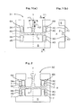
- Fig. 1 shows a top view and a sectional view of an embodiment of a piezoelectric/electrostrictive device of the present invention.
- Fig. 2 shows a top view of another embodiment of a piezoelectric/electrostrictive device of the present invention.
- Fig. 3 shows a top view of still another embodiment of a piezoelectric/electrostrictive device of the present invention.
- Fig. 4 shows a top view of still another embodiment of a piezoelectric/electrostrictive device of the present invention.
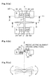
- Figs. 5 show a top view, sectional view, and shift illustration of still another embodiment of a piezoelectric/electrostrictive device of the present invention.
- Fig. 6 shows a top view and a sectional view of still another embodiment of a piezoelectric/electrostrictive device of the present invention.
- Fig. 7 shows a top view of still another embodiment of a piezoelectric/electrostrictive device of the present invention.
- Fig. 8 shows a top view of still another embodiment of a piezoelectric/electrostrictive device of the present invention.
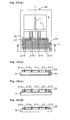
- Figs. 9 show a top view and sectional view of still another embodiment of a piezoelectric/electrostrictive device of the present invention.
- Figs. 10 show a top view and a sectional view of a mode having a detailed structure of the piezoelectric/electrostrictive device shown in Fig. 9.
- Fig. 11 shows a top view of a shape of a sheet member used to fabricate a piezoelectric/electrostrictive device of the present invention.
- Fig. 12 shows a perspective view of an embodiment of a piezoelectric element arranged on a piezoelectric/electrostrictive device of the present invention.
- Fig. 13 shows a perspective view of another embodiment of a piezoelectric element arranged on a piezoelectric/electrostrictive device of the present invention.
- Fig. 14 shows a perspective view of still another embodiment of a piezoelectric element arranged on a piezoelectric/electrostrictive device of the present invention.
- Fig. 15 shows an explanatory view of an example of a method for finishing a piezoelectric element of a piezoelectric/electrostrictive device of the present invention.
- Fig. 16 shows an example of a perspective view of the structure of a conventional piezoelectric/electrostrictive device (piezoelectric actuator).
- Fig. 17 shows a top view of still another embodiment of a piezoelectric/electrostrictive device of the present invention.
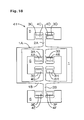
- Fig. 18 shows a top view of still another embodiment of a piezoelectric/electrostrictive device of the present invention.
- Fig. 19 shows a top view of still another embodiment of a piezoelectric/electrostrictive device of the present invention.
- Fig. 1(a) shows a top view of an embodiment of a first piezoelectric/electrostrictive device (hereafter referred to as "device") 31 and Fig. 1(b) shows a sectional view of a plane passing through Y1 axis and vertical to plane X-Y, that is, a sectional view of the cross section of the device 31 in plane Y-Z viewed from the X-axis direction (hereafter, the sectional view of Fig. 1(b) is expressed as "arrow AA view on Y1 axis”) .
- connection plate 2 of the device 31 in its longitudinal direction (X-axis direction) is held by two diaphragms 3A and 3B and the other end of the plate 2 is held by other two diaphragms 3C and 3D, these ends are spanned between the bottoms of faced concave portions 6A and 6B formed on a substrate 5.
- piezoelectric elements 4A to 4D are respectively arranged on one-side plane surfaces of diaphragms 3A to 3D, the diaphragms 3A to 3D are connected to the sides and bottoms of the concave portions 6A and 6B, and a fixing plate 1 is connected to a connection plate 2 so that the longitudinal direction of the fixing plate 1 becomes parallel with the direction for the diaphragms 3A to 3D to hold the connection plate 2, that is, the Y-axis direction.
- the members of the fixing plate 1, connection plate 2, diaphragms 3A to 3D, and substrate 5 are connected at the side of each member and formed into one body.
- electrode leads are arranged on piezoelectric elements 4A to 4D from electrodes for forming the piezoelectric elements 4A to 4D toward the substrate 5, they are omitted in Fig. 1.
- a fixing plate denotes a component for causing a predetermined displacement by driving a piezoelectric element and a member such as a magnetic head can be set to the fixing plate.
- a connection plate denotes a component for connecting a fixing plate with substrate and diaphragm
- a diaphragm denotes a component for generating a strain with piezoelectric elements arranged on the surface and transmitting the strain to a connection plate.
- the diaphragm also has a function for transmitting a strain generated due to a displacement of a fixing plate to a piezoelectric element when the strain is transmitted to a diaphragm through a connection plate.
- the substrate denotes a component for holding a driving portion (such as a connection plate, fixing plate, diaphragm, or piezoelectric element), on which various electrode terminals to be set to a measuring instrument are arranged and being provided for handling in practical use.
- a driving portion such as a connection plate, fixing plate, diaphragm, or piezoelectric element
- a concave portion formed on the substrate need not be a recess having a side vertical to a bottom or must not always have a portion opening in one direction. It is also possible that the bottom and the side have an angular portion having a curvature. That is, the concave portion denotes a portion having one bottom and two sides.
- a concave portion is formed by cutting out a part of the circumference of a substrate like a quadrangle.
- a quadrangular hole is formed in the substrate, it is possible to regard three out of four sides as a concave portion.
- the angle between the side and the bottom of a concave portion has an inclination as long as the driving characteristic of a device of the present invention can be obtained.
- a lamination-type piezoelectric element 88 is a typical one, which is obtained by forming a piezoelectric film 86 like a layer by positioning the film 86 between a first electrode 85 and a second electrode 87 as shown in Fig. 12.
- a piezoelectric element 94A having a comb-type electrodes structure in which a piezoelectric film 90 is formed on a diaphragm 89 and a first electrode 91 and a second electrode 92 form a predetermined-width gap 93 on the piezoelectric film 90.
- first electrode 91 and the second electrode 92 in Fig. 13 at the connection plane between the diaphragm 89 and piezoelectric film 90.
- a piezoelectric element 94B is preferably used in which the piezoelectric film 90 is embedded between the comb-type first electrode 91 and second electrode 92.
- a piezoelectric element having the comb-type electrodes shown in Figs. 13 and 14 it is possible to increase a displacement by decreasing the pitch D between the comb-type electrodes.
- the piezoelectric element shown in Figs. 12 to 14 can be applied to every device of the present invention to be mentioned later.
- the same phase/opposite phase for driving a piezoelectric element determines the direction of a strain generated in a piezoelectric element.
- the same phase represents driving a piezoelectric element so that a same-directional strain is obtained
- the opposite phase represents driving a piezoelectric element so that a reverse-directional strain is obtained or not driving a piezoelectric element without adding a signal, that is, driving a piezoelectric element so that a relatively-opposite-directional strain is obtained. Therefore, it is possible to constitute a group of piezoelectric elements by properly combining piezoelectric elements using the transversal effect (d 31 ) of an electric-field-induced strain and piezoelectric elements using the longitudinal effect (d 33 ) of the electric-field-induced strain.
- a piezoelectric element with a piezoelectric material requiring a polarization operation, it is possible to control a phase by setting the direction of a signal under driving to the direction same as or opposite to the polarity under polarization even for piezoelectric elements using all the same d 33 or d 31 .
- the device 31 has a structure in which the displacement of the connection plate 2 obtained by magnifying the displacement of the piezoelectric elements 4A to 4D is further magnified as the displacement of the fixed plate 1, it is possible to optionally set a response speed and the front-end displacement amount or generation force of the fixing plate 1 by variously selecting the length of the connection plate 2 and the length of the fixed plate.
- the device 31 for generating the above displacement on the fixing plate 1 it is preferable that the device 31 is connected with the connection plate 2 at the longitudinal center of the fixing plate 1 and the connection plate 2. In this case, because a displacement can be easily controlled, it is possible to obtain the maximum magnification rate of displacement.
- the diaphragms 3A to 3D and piezoelectric elements 4A to 4D it is not necessary for all of the diaphragms 3A to 3D and piezoelectric elements 4A to 4D to have the same shape.
- the piezoelectric elements 4A to 4D are provided for only one-side plane surfaces of the diaphragms 3A to 3D. However, it is also preferable to arrange piezoelectric elements on the other-side plane surfaces. In this case, it is needless to say that every piezoelectric element can be used for driving. It is possible to use the piezoelectric elements on one-side plane surfaces to drive the fixed plate 1 and those on the other-side plane surfaces as auxiliary elements. In this case, an auxiliary element represents a troubleshooting element, displacement confirmation/decision element, driving support element, or the like. By using an auxiliary element, it is possible to accurately drive a fixing plate.
- Auxiliary elements can be arranged also by forming the piezoelectric elements 4A to 4D provided for one-side plane surfaces of the diaphragms 3A to 3D as one pair of two elements divided in the X-axis direction.
- piezoelectric elements at the side close to the joint between the fixing plate 1 and connection plate 2 are used as driving elements and the others are used as auxiliary elements.
- To divide one piezoelectric element it is possible to use either of a method of arranging one piezoelectric element and thereafter dividing it through laser-beam machining and a method of first dividing one piezoelectric element into pairs of elements and then arranging them.
- the top view of Fig. 2 shows another embodiment of a device of the present invention.
- diaphragms 3A to 3D are respectively connected with only the sides of concave portions 6A and 6B, but they are not connected with the bottoms of the concave portions 6A and 6B.
- a gap 7 is formed between the bottoms of the concave portions 6A and 6B on one hand and the diaphragms 3A to 3D on the other respectively.
- the diaphragms 3A to 3D are connected with the sides of the concave portions 6A and 6B in the direction (Y-axis direction) for at least the diaphragms 3A to 3D to hold the connection plate 2.
- Y-axis direction Y-axis direction
- the shape of the fixing plate 1 is not restricted. It is possible to set the shape of the fixing plate 1 by considering the shape and weight of an element or sensor to be set to the front end of the fixing plate 1.
- Fig. 3 shows a top view of still another embodiment of a device of the present invention.
- a device 33 has a structure in which a notch 8 is provided for the joint between the fixing plate 1 and the connection plate 2 of the device 31.
- the in-plane rotation displacement of the fixing plate 1 of the device 31 previously shown in Fig. 1 is mainly generated in accordance with a bending displacement in the plane X-Y of the connection plate 2. Therefore, the in-plane rotation displacement is a displacement in which a connection angle between the connection plate 2 and the fixing plate 1 is almost kept.
- the notch 8 is formed like the case of the device 33 shown in Fig. 3, it is possible to convert a bending displacement of the connection plate 2 into a rotation displacement for further changing connection angles between the fixing plate 1 and the connection plate 2 at the connection position between the connection plate 2 and the fixing plate 1. As a result, it is possible to increase a displacement of the fixing plate 1. That is, the device 31 shown in Fig. 1 is used by magnifying displacement of the piezoelectric elements 4A to 4D mainly into a bending displacement of the connection plate 2 and the device 33 shown in Fig. 3 has a structure in which a displacement magnified to a bending displacement of the device 33 is further magnified as a rotation displacement, in a way, a two-step magnification mechanism can be effectively shown.
- the notch 8 it is preferable to form the notch 8 so as to increase the width-directional distance of the connection plate 2, that is, the Y-axis-directional distance up to the inside the fixing plate 1 and it is preferable to decrease the width of the notch 8, that is, the X-axis-directional distance of the notch 8.
- Fig. 4 shows a top view of still another embodiment of a device of the present invention.
- the arranged state of diaphragms of a device 34 is the same as the case of the device 32 described above.
- the device 34 has a structure in which a connection plate 2 is divided into two plates in the X-axis direction which is the spanning direction of the connection plate 2, a gap 9 is formed at the central portion of the connection plate 2, and a fixing plate 1 is connected to the plane surface of the connection plate 2 so as to cross the gap 9.
- the fixing plate 1 by preparing the fixing plate 1 as a separate body, such an advantage is obtained that it is possible to widen the range for selecting the material and shape of the fixing plate 1 according to the purpose of use.
- the connection plate 2 because the connection plate 2 must be connected with the fixing plate 1 by an adhesive or the like, the reliability is slightly deteriorated.
- the device 34 it is possible to form a notch 8 same as that of the device 33 at an end of the fixing plate 1 at a position crossing the divided connection plate 2, that is, at the gap 9.
- FIG. 5(a) shows a top view of still another embodiment of a device of the present invention.
- a device 35 has a structure in which a fixing plate 1 is connected to a connection plate 2 so as to intersect with the connection plate 2.
- Fig. 5(b) is an arrow-AA view at the Y1 axis, in which a pair of diaphragms (diaphragms 3C and 3D) for holding the connection plate 2 are each connected with the connection plate 2 at positions shifted in the thickness direction (Z-axis direction) of the connection plate 2.
- Fig. 6(a) shows a top view of a device 36 in which a notch 10 is formed on a connection plate 2 between the connection part of the connection plate 2 and the substrate 5 and the connection part of the connection plate 2 and the diaphragms 3A to 3D and Fig. 6(b) shows an arrow-AA view on X-axis.
- a notch 10 By forming the notch 10, it is possible to efficiently operate a fixing plate 1. When forming the notch 10, the operation efficiency is further improved by decreasing the thickness of the connection plate 2.
- the shape of the notch 10 is not restricted as long as the width and/or thickness of the notch 10 is decreased.
- a device 37 shown in Fig. 7 has a mode in which a connection plate 2 is divided into two plates in the longitudinal direction (Y-axis direction) of a fixing plate 1 and moreover, each of the divided connection plates 2 is divided into two plates in the spanning direction of each connection plate 2. Therefore, the fixing plate 1 is connected to either-side plane of the connection plate 2 so as to resultantly cross four connection plates 2.
- the connection plates 2 and the fixing plate 1 can be integrally formed and the connection plate 2 can be divided into three parts or more.
- connection plate in the longitudinal direction (Y-axis direction) of a fixing plate in the case of the present invention also includes a case in which a plurality of connection plates are arranged in the Y-axis direction through a gap without changing Y-axis-directional widths of the connection plates in addition to a case in which a connection plate is divided and a gap is formed and thereby, the Y-axis-directional width of newly formed connection plates is decreased.
- the device 37 has a mode in which piezoelectric elements 4A to 4D respectively drive one connection plate 2 through corresponding diaphragms 3A to 3D. Therefore, it is possible to obtain a plurality of points (joints) for making strains of the piezoelectric elements 4A to 4D work on the fixing plate 1. For example, by driving the piezoelectric elements 4A and 4D at the same phase and the piezoelectric elements 4B and 4C at a phase opposite to the case of the piezoelectric elements 4A and 4D, it is possible to make the fixing plate 1 efficiently generate a displacement of in-plane rotation mode.
- connection plates 2 it is possible to span a flat member thinner than the connection plates 2 between the connection plates 2 in the Y-axis direction.
- the relative displacement amount of the fixing plate 1 decreases compared to the case of not spanning the flat member, it is possible to operate the fixing plate 1 at a higher response speed because the rigidity is improved.
- Fig. 8 shows a top view of a device 38 in which a fixing plate 1 is integrally connected to two connection plates formed by being divided in the longitudinal direction of the fixing plate 1, a hinge portion 12 is provided for the fixing plate 1 from the joint between the fixing plate 1 and a connection plate 2 toward the longitudinal direction of the fixing plate 1, and moreover a notch 8 is formed on the joint between the fixing plate 1 and the connection plate 2.
- FIG. 9 shows still another embodiment of a device of the present invention.
- a device 39 is a mode in which the diaphragms 3A and 3C are removed from the above described device 32 when using two diaphragms 3A and 3B as shown in Fig. 9(a).
- the device 39 has a structure in which a connection plate 2 is spanned between the sides of a concave portion 6 formed on a substrate 5, two diaphragms 3A and 3B on which piezoelectric elements 4A and 4B are arranged are spanned between the connection plate 2 and the bottom of the concave portion 6 of the substrate 5, and a fixing plate 1 is connected to the connection plate 2 so that the longitudinal direction of the fixing plate 1 becomes parallel with the spanning direction (Y-axis direction) of the diaphragms 3A and 3B.
- the diaphragms 3A and 3B are normally arranged at positions symmetric to the longitudinal-direction axis (Y-axis) of the fixing plate 1. Moreover, it is possible to span two diaphragms or more between the connection plate 2 and the bottom of the concave portion 6.
- Figs. 9(b) to 9 (d) show an arrow-AA view on the Y1 axis showing a mode of the diaphragm 3B preferably adopted for the device 39.
- the mode of the diaphragm 3B is also applied to the diaphragm 3A.
- Fig. 9(b) shows a mode in which the diaphragm 3B is spanned between the vicinities of the surfaces of the connection plate 2 and the substrate 5.
- Fig. 9(c) shows a structure in which a pair of diaphragms 3B and 3C constituted so that plane surfaces are faced each other are spanned between the connection plate 2 and the substrate 5.
- another diaphragm 3D is provided for the diaphragm 3A so as to form a pair, and the fixing plate is driven by the total of four diaphragms.
- Fig. 9(d) shows a mode in which the diaphragm 3B is arranged at the central portion of the connection plate 2 in its thickness direction.
- a connection plate is held by a pair of diaphragms facing in the thickness direction of the connection plate.
- a connection plate is held by two diaphragms at the central portion of the connection plate in its thickness direction.
- Fig. 17 shows a top view of a device 40 constituted by connecting two devices 33 shown in Fig. 3 previously described.
- a fixing plate 1A driven by piezoelectric elements 4A to 4D is connected with a fixing plate 1B driven by piezoelectric elements 4E to 4H and thus, an integral fixing plate 1 is formed.
- the structure it is possible to generate a large amount of displacement and moreover increase the driving force of the device. Therefore, when securing other devices such as various sensors and magnetic heads to the fixing plate, it is easy to properly select the structure of the device 33 or the structure of the connected device 40 in accordance with the size or mass of the device.
- the device 40 has features of reducing unnecessary residual vibrations of the fixed plate 1 generated under a high-speed operation by driving one connected device (e.g. fixed plate-1B side) for braking at a predetermined timing and realizing high-speed positioning from the viewpoint of controlling a displacement and vibration.
- one connected device e.g. fixed plate-1B side
- connection between devices is not restricted to the case of using the device 33.
- This can be applied to the devices 31 to 39 shown in Figs. 1 to 9.
- a device 41 shown by a top view in Fig. 18 is constituted by connecting the device 35 shown in Fig. 5. Therefore, it is possible to generate a displacement of the rotation mode about the longitudinal axis of the connection plates 2A and 2B, increase a driving force, and brake the motion of the fixing plate 1.
- Fig. 19 shows a top view of a device 42 obtained by connecting four devices 33 shown in Fig. 3.
- the device 42 has, in other words, a structure obtained by connecting two devices 40 shown in Fig. 17 so that they are symmetric to X-axis.
- this structure it is possible to generate purer X-axis-directional and Y-axis(Y1-axis and Y2-axis)-directional displacement with a large force.
- Embodiments of the present invention are described above mainly on the structures of devices, in which various displacement modes of a fixing plate, that is, the in-plane rotation displacement mode, uniaxial displacement mode, and rotation displacement mode represent that the displacement direction of the fixing plate is predominant in each described direction but having directional components other than the above is not completely excluded.
- various displacement modes of a fixing plate that is, the in-plane rotation displacement mode, uniaxial displacement mode, and rotation displacement mode represent that the displacement direction of the fixing plate is predominant in each described direction but having directional components other than the above is not completely excluded.
- it is preferable to use a three-dimensional shiftlessness or a uniaxial displacement and in-plane rotation displacement so as to keep the interval (gap) between a head and a recording medium constant.
- a piezoelectric element has a unimorph structure.
- a piezoelectric element it is also possible for a piezoelectric element to have a bimorph structure.
- the number of diaphragms or the number of piezoelectric elements to be arranged can be optionally selected as long as it is not deviated from the design rules of the above devices.
- a device of the present invention is, as described above, not only used as an active element such as a displacing element or a vibrator to be driven by a piezoelectric element, but also used for various sensors as a passive element such as an acceleration sensor or impact sensor. Particularly, in the case of detection of acceleration, it is possible to easily improve the detection sensitivity by providing an inertial mass such as a weight for the front end of a fixing plate to increase the weight of the front end.
- Fig. 10(a) shows a top view of an embodiment in which electrode leads 21A to 21D are provided for piezoelectric elements 4A and 4B arranged on the device 39, an insulating coating layer 22 is provided for the piezoelectric elements 4A and 4B and the electrode leads 21A to 21D, and moreover a shielding layer 23 is formed so as to cover the insulating coating layer 22.
- Figs. 10B to 10D are arrow-AA views on the X1 axis in Fig. 10(a), showing different embodiments.
- the insulating coating layer 22 has a function for effectively preventing the piezoelectric elements 4A and 4B and the electrode leads 21A to 21D from being short-circuited when using a fixing plate 1 and/or the piezoelectric elements 4A and 4B in a liquid environment or a humidified environment.
- the shielding layer 23 has functions for cutting off external electromagnetic waves to preferably secure a displacing accuracy when operating a device at a high frequency or when detecting high-frequency vibrations and moreover, preventing erroneous operations and noises.
- Modes for arrangement of the shielding layer 23 include not only a mode for forming a substrate 5 so as to hold the substrate 5 as shown in Fig. 10(b) but also a mode for enclosing only the wiring portion on the substrate 5 as shown in Fig. 10(c) and a mode for shielding the wiring portion with only the upper-piece side as shown in Fig. 10(d). Particularly, the modes for entirely shielding the wiring portion are preferable as shown in Figs. 10(b) and 10(c).
- electrical connection of the shielding layer 23 formed on each face of the substrate 5 is secured by using a through-hole 24 formed on the substrate 5. However, it is also possible to secure the electrical connection by using the sides of the substrate 5. Details of materials preferably used to form the insulating coating layer 22 and shielding layer 23 are described together with device-forming materials to be mentioned later.
- Ceramics is preferably used for a substrate, fixing plate, connection plate, and diaphragm.
- fully-stabilized zirconia, partially-stabilized zirconia, alumina, magnesia, and silicon nitride are listed.
- full-stabilized zirconia and partially-stabilized zirconia are most preferably used because they have a large mechanical strength, a high toughness, and a small reactivity with a piezoelectric material and electrode materials even in the form of a thin plate.
- an additive such as alumina or titania to at least the diaphragm.
- the thickness and shape of a fixing plate of a device of the present invention are not restricted and therefore, the fixing plate is properly designed in accordance with its purpose. Moreover, the thickness of a substrate is properly determined by considering the operability. However, it is preferable to set the thickness of a diaphragm to 3 to 20 ⁇ m and the total thickness of a diaphragm and a piezoelectric element to 15 to 60 ⁇ m.
- connection plate it is preferable to set the thickness of a connection plate to 20 to 600 ⁇ m, the width of the connection plate to 30 to 500 ⁇ m, and the aspect ratio [width (Y-axis-directional length)/thickness ⁇ Z-axis(axis vertical to both X- and Y-axes)-directional length ⁇ ] of the connection plate in a range of 0.1 to 15. Particularly, it is preferable to set the aspect ratio in a range of 0.1 to 7 in order to make a displacement in the plane X-Y more predominant.
- a piezoelectric ceramics formed like a film is preferably used as a piezoelectric film of a piezoelectric element.
- electrostrictive ceramics, ferroelectric ceramics, or anti-ferroelectric ceramics it is possible to use a material requiring or not requiring polarization.
- a material having a small strain hysteresis because the linearity between the displacement amount of a fixing plate and a applying voltage or output voltage is important. Therefore, it is preferable to use a material of 10 kV/mm or less as a coercive electric field.
- piezoelectric ceramics the following are listed: lead zirconate, lead titanate, lead magnesium niobate, lead nickel niobate, lead zinc niobate, lead manganese niobate, lead antimony stannate, lead manganese tungstate, lead cobalt niobate, and barium titanate, and ceramics containing a component obtained by combining any ones of the above material.
- the present invention preferably uses a material consisting essentially of lead zirconate, lead titanate, and lead magnesium niobate as a major component.
- a material consisting essentially of lead zirconate, lead titanate, and lead magnesium niobate as a major component and containing lanthanum and strontium by adjusting the coercive electric field or piezoelectric characteristic.
- the electrode of a piezoelectric element is constituted a metal that is kept solid-state at room temperature and superior in conductivity.
- it is a single metal such as aluminum, titanium, chromium, iron, cobalt, nickel, copper, zinc, niobium, molybdenum, ruthenium, palladium, rhodium, silver, tin, tantalum, tungsten, iridium, platinum, gold, or lead or an alloy made by combining any ones of these metals.
- cermet made by dispersing the material of a piezoelectric film or diaphragm in the above metals.
- the material of the electrode of a piezoelectric element is determined depending on a piezoelectric-film forming method. For example, to form a first electrode on a diaphragm and then, a piezoelectric film on the first electrode through heat-treatment (firing), it is necessary to use a metal having high melting point such as platinum that is not changed at a firing temperature for the first electrode. However, because a second electrode formed on a piezoelectric film after the piezoelectric film is sintered can be formed at a low temperature, it is possible to use a metal having low melting point such as aluminum.
- first and second electrodes 91 and 92 are formed by co-firing (firing at one time for integration).
- a metal withstanding the sintering temperature of a piezoelectric film for both first and second electrodes.
- first and second electrodes 91 and 92 are formed on a piezoelectric film 90, it is possible to form the electrodes 91 and 92 by using the same metal having low-melting point.
- it is possible to properly select preferable electrodes as first and second electrodes by depending on a piezoelectric-film forming temperature represented by a piezoelectric-film sintering temperature and a piezoelectric-element structure.
- an electrode lead can be formed simultaneously with an electrode of a piezoelectric element. Furthermore, it is possible to form an electrode lead on a diaphragm simultaneously with a piezoelectric element and then, form an electrode lead on a substrate by various methods such as the sputtering method and screen printing method.
- insulating glass or resin is used as the material of an insulating coating layer to be formed on a piezoelectric element and an electrode lead.
- resin rather than glass.
- one of the following fluorocarbon polymer superior in chemical stability is preferably used: polytetrafluoroethylene based Teflon (Teflon PTFE made by Du Pont), polytetrafluoroethylene-hexafluoro-propylene copolymer based Teflon (Teflon FEP), polytetrafluoroethylene-perfluoroalkylvinylether copolymer ethylene-tetrafluoride-based Teflon (Teflon PFA), and PTFE/PFA composite Teflon.
- silicone resin particularly, thermosetting silicone resin
- silicone resin is also preferably used.
- epoxy resin or acrylic resin correspondingly to the purpose.
- an insulating coating layer When forming an insulating coating layer, one of various metals such as gold, silver, copper, nickel, and aluminum is preferably used as the material of a shielding layer formed on an insulating coating layer. Moreover, it is possible to use any one of the above-described metallic materials used for an electrode or the like of a piezoelectric element. Furthermore, it is possible to use conductive paste made by mixing metallic powder with resin.
- a device fabrication method of the present invention is described below by using the above device 31 as an example.
- Other devices 32 to 39 can be also fabricated by the same method.
- a device is constituted with members including a fixing plate, it is possible to fabricate the device by connecting components made of various materials prepared as separate bodies. In this case, however, there is a problem on the reliability because the productivity is low and a joint is easily damaged. Therefore, in the case of the present invention, the green-sheet laminating method using ceramics powder as a material is preferably adopted.
- slurry is first prepared by adding and mixing binder, solvent, and dispersant to ceramics powder such as zirconia and then slurry is degassed, and then form a green sheet or green tape having a predetermined thickness by the reverse roll coater method or doctor blade method or the like. Then, various green sheet members (hereafter referred to as "sheet members") shown in Fig. 11 are manufactured by punching the green sheet with a die.
- a sheet member 51 is a member serving as a substrate 5, a connection plate 2, a fixing plate 1, and diaphragms 3A to 3D after firing or sintering the sheet member 51. At this point of time, however, the sheet member 51 is formed as a single plate in which those shapes are unclear. This is, as described above, because it is preferable to form the diaphragms 3A to 3D at a small thickness of 3 to 20 ⁇ m, and therefore, it is preferable to cut off unnecessary portions of the sheet member 51 through laser-beam processing after firing it compared to the case of forming the shapes of the above members on the sheet member 51 under a green sheet state because the shape accuracy is preferably kept.
- a sheet member 52 is a member serving as the substrate 5 and moreover for forming the fixing plate 1 and the connection plate 2 so that they become thicker than the diaphragms 3A to 3D, on which a hole 55, the fixing plate 1 and the connection plate 2 are formed. It is also possible to form a notch 8 at the joint between the fixed plate 1 and the connection plate 2. Desired thicknesses of the fixing plate 1 and the connection plate 2 are obtained by superimposing a predetermined number of sheet members 52 each other. To form the fixing plate 1 thinner than the connection plate 2, it is possible to manufacture sheet members respectively obtained by removing only a portion serving as the fixing plate 1 from the sheet member 52 and superimpose them each other.
- the sheet member 53 with the hole 55 formed on it is a member serving as the substrate 5. By superimposing a predetermined number of sheet members, a desired thickness can be obtained.
- a green layered product is manufactured by superimposing these sheet members 51 to 53 in order while positioning the members 51 to 53 by using a reference hole 54 and uniting them into one body by pressing under heating. Thereafter, the green layered product is sintered at a temperature of 1,200°C to 1,600°C. It is preferable to previously form piezoelectric elements 4A to 4D at positions of the sheet member 51 on which the diaphragms 3A to 3D are finally formed and then, sinter them integrally with the green layered product.
- the temperature for sintering a piezoelectric film is properly determined depending on a material constituting the piezoelectric film, it is generally set to 800°C to 1,400°C, preferably set to 1,000°C to 1,400°C.
- the composition of the piezoelectric film it is preferable to sinter the material of the piezoelectric film under the existence of the evaporation source of the material.
- the present invention preferably adopts the thick-film-forming method according to one of the screen printing method, dipping method, and electrophoresis in order to form a piezoelectric film.
- piezoelectric elements after sintering a formed green layered product under a predetermined condition, then printing a first electrode at a predetermined position on the surface of a sintered sheet member 21 and firing or sintering it, then printing and sintering a piezoelectric film, and moreover printing and firing or sintering a second electrode. Then, an electrode lead for connecting an electrode of a piezoelectric element continuously formed to a measuring instrument is printed and fired.
- each member and electrode lead of a piezoelectric element by selecting a proper material, it is possible to successively print each member and electrode lead of a piezoelectric element and integrally sinter them at one time. On the other hand, it is possible to form a piezoelectric film and then, form each electrode at a low temperature. Furthermore, it is possible to form each member and electrode lead of a piezoelectric element through the thin-film method such as the sputtering method or vapor evaporation method. In this case, heat treatment is not always necessary.
- a piezoelectric element By forming a piezoelectric element through a film-forming method, it is possible to integrally bond and arrange a piezoelectric element and a diaphragm without using an adhesive, secure the reliability and reproducibility, and simplify integration. In this case, it is also possible to form a proper pattern on a piezoelectric film. To form the pattern, it is possible to use the screen printing method, photolithography method, or laser-beam machining method, or a machining method such as the slicing method or ultrasonic machining method.
- the diaphragms 3A to 3D, fixing plate 1, and connection plate 2 or the notch 8 if necessary are formed at predetermined positions of a sintered layered product on which the piezoelectric elements 4A to 4D and electrode leads are formed.
- it is preferable to adjust a displacement amount by adjusting the shapes of the fixing plate 1 and connection plate 2 mainly formed with the sheet member 22 or the shapes of the diaphragms 3A to 3D formed with the sheet member 21 under such a processing.
- a predetermined displacing characteristic by setting the piezoelectric element 88 shown in Fig. 12 in which the second electrode 87 is used as an upper electrode and the first electrode 85 as a lower electrode and the piezoelectric film 86 is formed between the upper and lower electrodes as shown in Fig. 15 and thereafter, removing the upper electrode through the YAG fourth harmonic laser beam or mechanical machining and adjusting the available electrode area of the piezoelectric element 88 to adjust the electrical characteristic such as the impedance of a piezoelectric/electrostrictive device.
- the piezoelectric element 88 has the comb-shaped structure shown in Fig. 13 or 14, it is necessary to remove a part of one or both electrodes.
- machining it is possible to use one of such machining methods suitable for the size and shape of a driving or movable portion as the laser-beam machining using a YAG laser beam, second or third harmonic wave, excimer laser beam, or CO 2 laser beam, electron-beam machining, and dicing (machining), in addition to the machining using the above YAG fourth harmonic laser beam.
- machining such as cutting, grinding, laser-beam machining, punching using a punch, or ultrasonic machining is applied to the device before and after sintering it and the device is formed into a predetermined shape.
- An insulating coating layer formed on the piezoelectric elements 4A to 4D and a electrode lead of the device 31 thus fabricated can be formed through the screen printing method, coating method, or spraying method by using glass or resin.
- glass when using glass as a material, it is necessary to raise the temperature of the device up to approx. the softening point of the glass, and it is preferable to use resin because the resin is soft and requires only drying or curing at low temperature though a displacement or vibration may be decreased because the glass has a high hardness.
- either of fluorocarbon polymer and silicone resin is preferably used as the resin for an insulating coating layer.
- a shielding layer to be formed on an insulating coating layer is formed through a method not requiring heating such as the sputtering method when using various metals because it is difficult to perform heat-treatment or firing if the insulating coating layer is made of resin.
- conductive paste made of metallic powder and resin it is possible to preferably use the screen printing method or coating method.
- a piezoelectric/electrostrictive device of the present invention has features that the structure is simple and the device can be easily decreased in size and weight and it is not easily influenced by external harmful vibrations. Moreover, the device has features that accurate control is realized for both static displacement and dynamic displacement and a large amount of displacement can be easily obtained and moreover, when using the device as a sensor, the sensitivity can be raised. Furthermore, by using a simple fabrication method such as the green-sheet laminating method, an advantage is obtained that the device can be inexpensively fabricated while improving the reliability as an integral structure. Furthermore, an advantages is obtained that the allowable range for selecting a component material is wide and a preferable material can be used correspondingly to the purpose at any time. Therefore, when setting the device into various actuators and sensors, it realizes high-accuracy control and measurement and the device shows a superior advantage that it contributes to the decrease in size and weight.
Landscapes
- Physics & Mathematics (AREA)
- General Physics & Mathematics (AREA)
- Engineering & Computer Science (AREA)
- Mechanical Engineering (AREA)
- Measurement Of Mechanical Vibrations Or Ultrasonic Waves (AREA)
- General Electrical Machinery Utilizing Piezoelectricity, Electrostriction Or Magnetostriction (AREA)
- Micromachines (AREA)
- Measurement Of Levels Of Liquids Or Fluent Solid Materials (AREA)
- Apparatus Associated With Microorganisms And Enzymes (AREA)
- Mechanical Light Control Or Optical Switches (AREA)
- Supporting Of Heads In Record-Carrier Devices (AREA)
- Measuring Fluid Pressure (AREA)
- Piezo-Electric Or Mechanical Vibrators, Or Delay Or Filter Circuits (AREA)
Applications Claiming Priority (6)
| Application Number | Priority Date | Filing Date | Title |
|---|---|---|---|
| JP24307397 | 1997-09-08 | ||
| JP36136897 | 1997-12-26 | ||
| PCT/JP1998/003971 WO1999013518A1 (fr) | 1997-09-08 | 1998-09-04 | Dispositif piezoelectrique/electrostrictif |
| WOPCT/JP98/03971 | 1998-09-04 | ||
| US09/242,642 US6239534B1 (en) | 1997-09-08 | 1998-12-28 | Piezoelectric/electrostrictive device |
| US242642 | 1998-12-28 |
Publications (2)
| Publication Number | Publication Date |
|---|---|
| EP0996175A2 true EP0996175A2 (de) | 2000-04-26 |
| EP0996175A3 EP0996175A3 (de) | 2002-09-25 |
Family
ID=85685825
Family Applications (3)
| Application Number | Title | Priority Date | Filing Date |
|---|---|---|---|
| EP98941714A Expired - Lifetime EP0943903B1 (de) | 1997-09-08 | 1998-09-04 | Gewichtssensor und verfahren zur bestimmung der masse |
| EP98941716A Withdrawn EP0938143A4 (de) | 1997-09-08 | 1998-09-04 | Piezoelektrische/elektrostriktive anordnung |
| EP99307027A Withdrawn EP0996175A3 (de) | 1997-09-08 | 1999-09-03 | Piezoelektrische/elektrostriktive Anordnung |
Family Applications Before (2)
| Application Number | Title | Priority Date | Filing Date |
|---|---|---|---|
| EP98941714A Expired - Lifetime EP0943903B1 (de) | 1997-09-08 | 1998-09-04 | Gewichtssensor und verfahren zur bestimmung der masse |
| EP98941716A Withdrawn EP0938143A4 (de) | 1997-09-08 | 1998-09-04 | Piezoelektrische/elektrostriktive anordnung |
Country Status (6)
| Country | Link |
|---|---|
| US (8) | US6386053B1 (de) |
| EP (3) | EP0943903B1 (de) |
| JP (4) | JP3844784B2 (de) |
| CN (2) | CN1243604A (de) |
| DE (1) | DE69827767T2 (de) |
| WO (2) | WO1999013518A1 (de) |
Cited By (1)
| Publication number | Priority date | Publication date | Assignee | Title |
|---|---|---|---|---|
| EP1411560A3 (de) * | 2002-10-16 | 2006-03-22 | Matsushita Electric Industrial Co., Ltd. | Piezoelektrischer Aktuator und Plattenlaufwerk mit diesem |
Families Citing this family (100)
| Publication number | Priority date | Publication date | Assignee | Title |
|---|---|---|---|---|
| JP3844784B2 (ja) * | 1997-09-08 | 2006-11-15 | 日本碍子株式会社 | 圧電/電歪デバイス |
| EP1065735B1 (de) * | 1999-06-29 | 2007-03-07 | Siemens Aktiengesellschaft | Piezoaktor mit einer elektrisch leitenden Mehrschichtfolie |
| EP1279021A4 (de) * | 2000-04-05 | 2008-06-18 | Draper Lab Charles S | Vorrichtung und verfahren zur messung der masse einer substanz |
| US6760195B2 (en) * | 2000-04-17 | 2004-07-06 | Seagate Technology Llc | Intrinsically excitable actuator assembly |
| JP3376417B2 (ja) | 2000-04-20 | 2003-02-10 | 独立行政法人産業技術総合研究所 | 高周波数水晶振動子を用いた超微量質量の検出装置用校正方法 |
| JP4868270B2 (ja) * | 2000-05-26 | 2012-02-01 | 日立金属株式会社 | 圧電アクチュエータ素子 |
| EP1160885B1 (de) * | 2000-05-31 | 2010-08-18 | Denso Corporation | Piezoelektrisches Bauelement für eine Einspritzvorrichtung |
| DE10029444B4 (de) * | 2000-06-21 | 2004-07-22 | Leica Microsystems Heidelberg Gmbh | Optische Anordnung |
| US6851120B2 (en) * | 2000-07-13 | 2005-02-01 | Seagate Technology Llc | Micro-actuator structure for improved stability |
| JP2004527210A (ja) * | 2000-08-02 | 2004-09-09 | ザ ジョンズ ホプキンス ユニバーシティー | 内皮細胞発現パターンの評価法 |
| JP2002141569A (ja) * | 2000-08-03 | 2002-05-17 | Tokin Ceramics Corp | マイクロアクチュエータ素子 |
| JP4095439B2 (ja) * | 2000-10-20 | 2008-06-04 | 富士通株式会社 | 圧電アクチュエータ |
| US6689288B2 (en) | 2000-11-28 | 2004-02-10 | The United States Of America As Represented By The Administrator Of The National Aeronautics And Space Administration | Polymeric blends for sensor and actuation dual functionality |
| JP4587232B2 (ja) * | 2001-01-18 | 2010-11-24 | 日本碍子株式会社 | 圧電/電歪デバイスおよびその製造方法 |
| JP3485904B2 (ja) | 2001-04-24 | 2004-01-13 | 松下電器産業株式会社 | 音響変換器 |
| US7162918B2 (en) * | 2001-05-15 | 2007-01-16 | Baker Hughes Incorporated | Method and apparatus for downhole fluid characterization using flexural mechanical resonators |
| US7317989B2 (en) * | 2001-05-15 | 2008-01-08 | Baker Hughes Incorporated | Method and apparatus for chemometric estimations of fluid density, viscosity, dielectric constant, and resistivity from mechanical resonator data |
| EP1397661B1 (de) * | 2001-05-15 | 2008-09-10 | Baker Hughes Incorporated | Verfahren und vorrichtung zur bohrloch-fluid-charakterisierung unter verwendung mechanischer biegeschwingungsresonatoren |
| US6876129B2 (en) * | 2001-09-26 | 2005-04-05 | Mitsuba Corporation | Rotary actuator and method of controlling an actuator |
| US7011758B2 (en) * | 2002-02-11 | 2006-03-14 | The Board Of Trustees Of The University Of Illinois | Methods and systems for membrane testing |
| JP4305623B2 (ja) * | 2002-03-13 | 2009-07-29 | セイコーエプソン株式会社 | 振動子および振動型ジャイロスコープ |
| US7043969B2 (en) * | 2002-10-18 | 2006-05-16 | Symyx Technologies, Inc. | Machine fluid sensor and method |
| DE10260088A1 (de) * | 2002-12-19 | 2004-08-05 | Endress + Hauser Gmbh + Co. Kg | Vorrichtung zur Bestimmung und/oder Überwachung mindestens einer physikalischen Größe mit einem Piezoantrieb zur Schwingungserregung und -detektion |
| US7521257B2 (en) * | 2003-02-11 | 2009-04-21 | The Board Of Regents Of The Nevada System Of Higher Education On Behalf Of The University Of Nevada, Reno | Chemical sensor with oscillating cantilevered probe and mechanical stop |
| US7260980B2 (en) * | 2003-03-11 | 2007-08-28 | Adams Jesse D | Liquid cell and passivated probe for atomic force microscopy and chemical sensing |
| WO2005026678A1 (de) * | 2003-09-17 | 2005-03-24 | Kistler Holding Ag | Mehrschichtiges piezoelektrisches messelement und ein druck- oder kraftsensor umfassend ein solches messelement |
| US20060257286A1 (en) | 2003-10-17 | 2006-11-16 | Adams Jesse D | Self-sensing array of microcantilevers for chemical detection |
| WO2005043126A2 (en) * | 2003-10-27 | 2005-05-12 | Drexel University | Piezoelectric cantilever sensors |
| KR100613398B1 (ko) * | 2003-11-25 | 2006-08-17 | 한국과학기술연구원 | 캔틸레버 센서형 분석 시스템, 제조 방법 및 이를 이용한극미세 물질 감지 방법 |
| US20050148065A1 (en) * | 2003-12-30 | 2005-07-07 | Intel Corporation | Biosensor utilizing a resonator having a functionalized surface |
| US7500840B2 (en) * | 2004-03-23 | 2009-03-10 | Sintokogio, Ltd. | Apparatus for molding a mold and a metal used therefor |
| US7279131B2 (en) * | 2004-07-01 | 2007-10-09 | Uop Llc | Method and apparatus for mass analysis of samples |
| KR20060006269A (ko) * | 2004-07-15 | 2006-01-19 | 한국항공우주연구원 | 진동자의 주파수 변화 측정에 의한 질량 측정 시스템 및방법 |
| US7694346B2 (en) | 2004-10-01 | 2010-04-06 | Board Of Regents Of The Nevada System Of Higher Education On Behalf Of The University Of Nevada | Cantilevered probe detector with piezoelectric element |
| US20060217893A1 (en) * | 2005-01-07 | 2006-09-28 | Yanbin Li | Method for detecting an unknown contaminant concentration in a substance |
| JP4529889B2 (ja) * | 2005-02-10 | 2010-08-25 | セイコーエプソン株式会社 | 圧電振動体、圧電振動体の調整方法、圧電アクチュエータ、時計、電子機器 |
| US7221076B2 (en) * | 2005-07-15 | 2007-05-22 | Avago Technologies General Ip (Singapore) Pte. Ltd. | Multiple movements harmonic frequency actuator system |
| US7819011B2 (en) * | 2005-08-23 | 2010-10-26 | Georgia Tech Research Corporation | High-Q longitudinal block resonators with annexed platforms for mass sensing applications |
| DE102005050159A1 (de) * | 2005-10-19 | 2007-04-26 | Siemens Ag | Schwingungssensor |
| DE102006039858A1 (de) * | 2006-01-02 | 2007-07-12 | Ceramtec Ag Innovative Ceramic Engineering | Monolithisches Biegeelement |
| US7927288B2 (en) * | 2006-01-20 | 2011-04-19 | The Regents Of The University Of Michigan | In situ tissue analysis device and method |
| US8171795B1 (en) * | 2006-01-23 | 2012-05-08 | Drexel University | Self-exciting, self-sensing piezoelectric cantilever sensor for detection of airborne analytes directly in air |
| CN101371132B (zh) * | 2006-01-23 | 2013-05-01 | 德雷塞尔大学 | 自励、自感知压电悬臂梁传感器 |
| US7681449B2 (en) * | 2006-02-28 | 2010-03-23 | Exxonmobil Research And Engineering Company | Metal loss rate sensor and measurement using a mechanical oscillator |
| JP2007265570A (ja) * | 2006-03-29 | 2007-10-11 | Fujitsu Ltd | 微小変位機構及び磁気ディスク装置 |
| US8179257B2 (en) * | 2006-03-30 | 2012-05-15 | International Business Machines Corporation | Warning of hazardous conditions in monitored spaces using RFID technology |
| JP4807632B2 (ja) * | 2006-06-22 | 2011-11-02 | 独立行政法人産業技術総合研究所 | 検出センサ |
| US7569977B2 (en) * | 2006-08-02 | 2009-08-04 | Cts Corporation | Laser capacitance trimmed piezoelectric element and method of making the same |
| JP5205725B2 (ja) * | 2006-08-21 | 2013-06-05 | パナソニック株式会社 | 角速度センサ |
| WO2008028124A1 (en) * | 2006-09-01 | 2008-03-06 | The Board Of Trustees Of The University Of Arkansas | Methods and systems for detection of contaminants |
| JP5019120B2 (ja) * | 2007-03-16 | 2012-09-05 | 独立行政法人産業技術総合研究所 | 検出センサ |
| WO2008114603A1 (ja) * | 2007-03-16 | 2008-09-25 | National Institute Of Advanced Industrial Science And Technology | 検出センサ、振動子 |
| JP4962565B2 (ja) * | 2007-04-27 | 2012-06-27 | 株式会社村田製作所 | 共振素子および、その製造方法 |
| FR2916271B1 (fr) * | 2007-05-14 | 2009-08-28 | St Microelectronics Sa | Circuit electronique permettant la mesure de masse de materiau biologique et procede de fabrication |
| FR2924422B1 (fr) * | 2007-11-30 | 2009-12-25 | Commissariat Energie Atomique | Dispositif a detection par jauge de contrainte piezoresistive suspendue comportant une cellule d'amplification de contrainte. |
| US20090238955A1 (en) * | 2008-03-20 | 2009-09-24 | E. I. Du Pont De Nemours And Company | Processes for the manufacture of barium titanate capacitors on nickel foils |
| CN101576404B (zh) * | 2008-05-08 | 2011-04-20 | 瑞鼎科技股份有限公司 | 振荡器、质量测量系统以及质量测量方法 |
| JP5292954B2 (ja) * | 2008-07-04 | 2013-09-18 | 株式会社ニコン | 振動アクチュエータ及びレンズ鏡筒 |
| DE102008046336A1 (de) * | 2008-09-09 | 2010-03-11 | Osram Gesellschaft mit beschränkter Haftung | LTCC-Schichtstapel |
| JP2010078334A (ja) * | 2008-09-24 | 2010-04-08 | National Institute Of Advanced Industrial Science & Technology | 検出センサ、振動子 |
| US7960201B2 (en) * | 2009-01-29 | 2011-06-14 | Emcore Solar Power, Inc. | String interconnection and fabrication of inverted metamorphic multijunction solar cells |
| FR2951826B1 (fr) * | 2009-10-23 | 2012-06-15 | Commissariat Energie Atomique | Capteur a detection piezoresistive dans le plan |
| US20110133755A1 (en) * | 2009-12-08 | 2011-06-09 | Delphi Technologies, Inc. | System and Method of Occupant Detection with a Resonant Frequency |
| US20110184313A1 (en) * | 2010-01-22 | 2011-07-28 | The Regents Of The University Of Michigan | Cauterization Device and Method of Cauterizing |
| JP5231495B2 (ja) * | 2010-03-10 | 2013-07-10 | 日本電波工業株式会社 | 微生物の検出方法及び微生物検出装置 |
| FR2957416B1 (fr) * | 2010-03-12 | 2012-04-20 | Thales Sa | Dispositif de quantification du degazage d'un equipement place dans une enceinte a vide |
| JP5565856B2 (ja) * | 2010-03-24 | 2014-08-06 | セイコーインスツル株式会社 | ダイアフラム、ダイアフラムバルブ、及びダイアフラムの製造方法 |
| IT1403287B1 (it) * | 2010-12-23 | 2013-10-17 | Associazione La Nostra Famiglia Irccs Eugenio Medea | Dispositivo per il rilevamento di sollecitazioni meccaniche in ambiente nmr |
| US9222867B2 (en) | 2011-01-05 | 2015-12-29 | Brian L. Norling | Resonant micromachined biochemical sensor |
| AT511330B1 (de) * | 2011-06-03 | 2012-11-15 | Piezocryst Advanced Sensorics | Sensor für die messung von druck und/oder kraft |
| US12218609B2 (en) * | 2012-05-11 | 2025-02-04 | The Regents Of The University Of California | Virus-based piezoelectric energy generation |
| JP2014000491A (ja) * | 2012-06-15 | 2014-01-09 | Canon Inc | 振動型駆動装置、医療装置、及び医療システム |
| GB201219029D0 (en) * | 2012-10-23 | 2012-12-05 | Liverpool John Moores University | Electromagnetic wave sensing |
| JP6086347B2 (ja) | 2013-02-16 | 2017-03-01 | 国立大学法人信州大学 | 共振型質量センサ |
| WO2016052116A1 (ja) * | 2014-10-03 | 2016-04-07 | 住友精密工業株式会社 | シャッタ装置及び駆動装置 |
| CN106092387B (zh) | 2015-04-30 | 2019-11-22 | 意法半导体股份有限公司 | 用于检测诸如冲击、加速度、旋转力等平面内的力的集成压电传感器 |
| DE102016104803B4 (de) * | 2016-03-15 | 2018-01-18 | Physik Instrumente (Pi) Gmbh & Co. Kg | Piezoelektrischer Schreitantrieb |
| WO2018088340A1 (ja) * | 2016-11-11 | 2018-05-17 | 株式会社村田製作所 | 振動装置 |
| CN109923685B (zh) * | 2016-11-18 | 2023-11-10 | Vega格里沙贝两合公司 | 压电发射和接收装置及其制造方法,以及振动传感器 |
| CN106784297B (zh) * | 2016-12-09 | 2020-09-25 | 苏州攀特电陶科技股份有限公司 | 压电陶瓷致动片及其制备方法 |
| US10952654B2 (en) | 2017-03-14 | 2021-03-23 | International Business Machines Corporation | PH sensitive surgical tool |
| JP2018155576A (ja) * | 2017-03-17 | 2018-10-04 | 太陽誘電株式会社 | 検出素子及び検出装置 |
| DE102017214786A1 (de) | 2017-08-23 | 2019-02-28 | Infineon Technologies Ag | MEMS-Sensoren, Verfahren zum Bereitstellen derselben und Verfahren zum Messen eines Fluidbestandteils |
| CA3110605A1 (en) * | 2017-12-24 | 2019-06-27 | Shekel Scales (2008) Ltd | Planar load cell assembly |
| RU180725U1 (ru) * | 2018-01-22 | 2018-06-21 | Открытое акционерное общество "ФОМОС-МАТЕРИАЛС" | Высокотемпературный масс-чувствительный элемент для пьезорезонансных датчиков |
| JP2021526651A (ja) | 2018-05-16 | 2021-10-07 | シェケル スケールズ(2008)リミテッド | 計量ロードセルおよびそれらを棚において利用する構成 |
| WO2020003221A1 (en) | 2018-06-28 | 2020-01-02 | Shekel Scales (2008) Ltd | Systems and methods for weighing products on a shelf |
| WO2019234692A1 (en) | 2018-06-06 | 2019-12-12 | Shekel Scales (2008) Ltd | Systems and methods for weighing products on a shelf |
| CN108827431B (zh) * | 2018-06-06 | 2020-08-14 | 南京邮电大学 | 一种基于opcl耦合的光机械腔质量传感器 |
| CN109248825A (zh) * | 2018-11-05 | 2019-01-22 | 大连理工大学 | 基于力反馈控制的微量高粘度胶液转移方法 |
| WO2020163595A1 (en) * | 2019-02-07 | 2020-08-13 | Butterfly Network, Inc | Bi-layer metal electrode for micromachined ultrasonic transducer devices |
| EP3715826B1 (de) * | 2019-03-26 | 2024-03-06 | Infineon Technologies AG | Sensorvorrichtung, partikelsensorvorrichtung und verfahren zur detektion der dichte eines partikelförmigen materials |
| US11684951B2 (en) | 2019-08-08 | 2023-06-27 | Bfly Operations, Inc. | Micromachined ultrasonic transducer devices having truncated circle shaped cavities |
| KR20220050550A (ko) * | 2020-10-16 | 2022-04-25 | 경희대학교 산학협력단 | 정전 발전기 |
| CN112282478B (zh) * | 2020-10-16 | 2022-05-13 | 广东电网有限责任公司 | 一种承力调整装置及输电铁塔 |
| JP7528804B2 (ja) * | 2021-02-03 | 2024-08-06 | 株式会社デンソー | 圧電素子、圧電装置、および圧電素子の製造方法 |
| TWI807333B (zh) * | 2021-03-19 | 2023-07-01 | 美律實業股份有限公司 | 電子裝置 |
| US11818955B2 (en) * | 2021-08-26 | 2023-11-14 | City University Of Hong Kong | Method for forming piezoelectric films on surfaces of arbitrary morphologies |
| CN114482987B (zh) * | 2021-12-24 | 2024-08-27 | 中国船舶重工集团公司第七一五研究所 | 一种低频多模偶极子发射换能器 |
| CN115037185B (zh) * | 2022-07-18 | 2024-03-12 | 西安交通大学 | 基于压电充放电原理的结构形状调节机构与断电保形方法 |
Family Cites Families (57)
| Publication number | Priority date | Publication date | Assignee | Title |
|---|---|---|---|---|
| NL278407A (de) | 1961-05-15 | |||
| US3581579A (en) * | 1968-07-17 | 1971-06-01 | Singer General Precision | Fluidic accelerometer |
| US3739202A (en) * | 1970-08-28 | 1973-06-12 | W Cady | Instrument for responding to mechanical vibration of acceleration andfor converting the same into electric energy |
| US4215570A (en) * | 1979-04-20 | 1980-08-05 | The United States Of America As Represented By The United States Department Of Energy | Miniature quartz resonator force transducer |
| US4383763A (en) * | 1979-09-12 | 1983-05-17 | Litton Systems, Inc. | Controllable mirrors |
| SE434438B (sv) | 1980-02-21 | 1984-07-23 | Gambro Engstrom Ab | Anordning for detektering av forekomsten av en given gaskomponent i en gasblandning |
| JPS58137317A (ja) * | 1982-02-09 | 1983-08-15 | Nec Corp | 圧電薄膜複合振動子 |
| DE3246201A1 (de) * | 1982-12-14 | 1984-06-14 | Wabco Westinghouse Fahrzeugbremsen GmbH, 3000 Hannover | Verfahren und einrichtung zur ermittlung des gewichtes eines fahrzeuges |
| US4517841A (en) | 1983-01-06 | 1985-05-21 | Sundstrand Data Control, Inc. | Accelerometer with beam resonator force transducer |
| JPS60133320A (ja) * | 1983-12-22 | 1985-07-16 | Ishida Scales Mfg Co Ltd | 荷重検出器 |
| US4685767A (en) * | 1984-02-27 | 1987-08-11 | Matsushita Electric Industrial Co., Ltd. | Fine adjustment apparatus for optical system lens |
| US4613782A (en) * | 1984-03-23 | 1986-09-23 | Hitachi, Ltd. | Actuator |
| JPS6146082A (ja) | 1984-08-10 | 1986-03-06 | Nippon Telegr & Teleph Corp <Ntt> | 圧電アクチユエ−タ |
| JPS61185982A (ja) * | 1985-02-14 | 1986-08-19 | Mitsubishi Electric Corp | セラミツク圧電材料 |
| JPS61231419A (ja) | 1985-04-08 | 1986-10-15 | Nok Corp | 有機物質の微量測定法 |
| JPS6264934A (ja) | 1985-09-17 | 1987-03-24 | Seiko Instr & Electronics Ltd | 水晶振動子バイオセンサ− |
| EP0215669A3 (de) | 1985-09-17 | 1989-08-30 | Seiko Instruments Inc. | Vorrichtung und Verfahren zur Analysierung von Biochemikalien, Mikroben und Zellen |
| JPS62201956A (ja) | 1986-02-28 | 1987-09-05 | Toyobo Co Ltd | ポリアミド組成物 |
| JPS62201956U (de) * | 1986-06-12 | 1987-12-23 | ||
| JPS6364640A (ja) * | 1986-09-06 | 1988-03-23 | Olympus Optical Co Ltd | アクチユエ−タ |
| JPS63200028A (ja) | 1987-02-17 | 1988-08-18 | Japan Atom Energy Res Inst | 圧電振動子を用いた重量測定法及び装置 |
| JPS63224275A (ja) | 1987-03-13 | 1988-09-19 | Ube Ind Ltd | 圧電たわみ素子 |
| JPS64351A (en) | 1987-06-18 | 1989-01-05 | Yanmar Diesel Engine Co Ltd | Unit injector driving device for internal combustion engine |
| JPS64351U (de) * | 1987-06-19 | 1989-01-05 | ||
| JPH07118146B2 (ja) | 1987-07-31 | 1995-12-18 | 株式会社富士通ゼネラル | 磁気記録再生装置 |
| JPS6435767U (de) * | 1987-08-26 | 1989-03-03 | ||
| US5079958A (en) * | 1989-03-17 | 1992-01-14 | Olympus Optical Co., Ltd. | Sensor having a cantilever |
| JP2936331B2 (ja) | 1989-06-29 | 1999-08-23 | 京セラ株式会社 | 固体電解質燃料電池用支持管 |
| JPH0334259U (de) * | 1989-08-10 | 1991-04-04 | ||
| GB8922601D0 (en) | 1989-10-06 | 1989-11-22 | Rolls Royce Plc | Thermal piezoelectric microbalance and method of using the same |
| JP2971916B2 (ja) | 1990-07-02 | 1999-11-08 | 東洋化工株式会社 | 樹脂系圧電素子の製造方法 |
| US5209119A (en) * | 1990-12-12 | 1993-05-11 | Regents Of The University Of Minnesota | Microdevice for sensing a force |
| US5323228A (en) * | 1991-04-22 | 1994-06-21 | Alliedsignal Inc. | Cavity length controller for ring laser gyroscope applications |
| US5351412A (en) * | 1991-06-11 | 1994-10-04 | International Business Machines Corporation | Micro positioning device |
| US5121180A (en) * | 1991-06-21 | 1992-06-09 | Texas Instruments Incorporated | Accelerometer with central mass in support |
| EP0549814B1 (de) * | 1991-07-23 | 1997-06-18 | Fujitsu Limited | Gerät zur feineinstellung eines kopfes |
| US5668303A (en) | 1992-04-30 | 1997-09-16 | Forschung E.V Fraunhofer-Gesellschaft Zur Foerderung Der Angewandten | Sensor having a membrane as part of an electromechanical resonance circuit forming receiver and transmitter converter with interdigital structures spaced apart from one another |
| JPH0670565A (ja) * | 1992-08-18 | 1994-03-11 | Olympus Optical Co Ltd | 超音波振動子及び超音波アクチュエータ |
| US5349844A (en) * | 1992-09-11 | 1994-09-27 | Trc Companies, Inc. | System and method for resonant filter mass monitoring |
| JPH06104503A (ja) | 1992-09-18 | 1994-04-15 | Sharp Corp | バイモルフ型圧電アクチュエータ |
| JP2542154B2 (ja) * | 1992-11-26 | 1996-10-09 | 山一電機株式会社 | 圧電アクチェ―タ― |
| DE69423667T2 (de) * | 1993-03-01 | 2000-11-23 | Murata Mfg. Co., Ltd. | Piezoelektrischer Vibrator und diesen verwendenden Beschleunigungssensor |
| US5708320A (en) * | 1994-10-28 | 1998-01-13 | Alps Electric Co., Ltd | Vibratory gyroscope |
| WO1996014687A1 (en) * | 1994-11-07 | 1996-05-17 | Matsushita Electric Industrial Co., Ltd. | Piezoelectric actuator and pyroelectric infrared-ray sensor using the same |
| DE4445642A1 (de) * | 1994-12-21 | 1996-06-27 | Marco Systemanalyse Entw | Piezoaktuatorisches Antriebs- bzw. Verstellelement |
| JP4210328B2 (ja) * | 1995-06-07 | 2009-01-14 | ナイキ,インコーポレイテッド | ポリエステルポリオールを含有するポリウレタンをベースとした物質からなる膜 |
| JP2709045B2 (ja) * | 1995-07-31 | 1998-02-04 | 有限会社ユーエスエム | 圧電駆動装置 |
| JPH09196682A (ja) | 1996-01-19 | 1997-07-31 | Matsushita Electric Ind Co Ltd | 角速度センサと加速度センサ |
| DE19613158A1 (de) * | 1996-04-02 | 1997-10-09 | Daetwyler Ag | Hochdynamischer piezoelektrischer Antrieb |
| JPH10136665A (ja) | 1996-10-31 | 1998-05-22 | Tdk Corp | 圧電アクチュエータ |
| US5827947A (en) | 1997-01-17 | 1998-10-27 | Advanced Technology Materials, Inc. | Piezoelectric sensor for hydride gases, and fluid monitoring apparatus comprising same |
| JP3434672B2 (ja) * | 1997-05-29 | 2003-08-11 | セイコーインスツルメンツ株式会社 | 小型回転式アクチュエータ及び小型回転式アクチュエータの共振周波数補正方法 |
| US5867302A (en) * | 1997-08-07 | 1999-02-02 | Sandia Corporation | Bistable microelectromechanical actuator |
| JP3844784B2 (ja) * | 1997-09-08 | 2006-11-15 | 日本碍子株式会社 | 圧電/電歪デバイス |
| WO1999025033A1 (en) * | 1997-11-12 | 1999-05-20 | Deka Products Limited Partnership | Piezo-electric actuator operable in an electrolytic fluid |
| JP3545269B2 (ja) | 1998-09-04 | 2004-07-21 | 日本碍子株式会社 | 質量センサ及び質量検出方法 |
| JP2000180250A (ja) * | 1998-10-09 | 2000-06-30 | Ngk Insulators Ltd | 質量センサ及び質量検出方法 |
-
1998
- 1998-09-04 JP JP51533499A patent/JP3844784B2/ja not_active Expired - Fee Related
- 1998-09-04 DE DE69827767T patent/DE69827767T2/de not_active Expired - Fee Related
- 1998-09-04 WO PCT/JP1998/003971 patent/WO1999013518A1/ja not_active Ceased
- 1998-09-04 JP JP51533399A patent/JP3298897B2/ja not_active Expired - Fee Related
- 1998-09-04 EP EP98941714A patent/EP0943903B1/de not_active Expired - Lifetime
- 1998-09-04 US US09/297,655 patent/US6386053B1/en not_active Expired - Fee Related
- 1998-09-04 EP EP98941716A patent/EP0938143A4/de not_active Withdrawn
- 1998-09-04 WO PCT/JP1998/003969 patent/WO1999013300A1/ja not_active Ceased
- 1998-09-04 US US09/214,110 patent/US6465934B1/en not_active Expired - Fee Related
- 1998-09-04 CN CN98801731.8A patent/CN1243604A/zh active Pending
- 1998-09-04 CN CN98801739.3A patent/CN1119628C/zh not_active Expired - Fee Related
- 1998-12-28 US US09/242,642 patent/US6239534B1/en not_active Expired - Fee Related
-
1999
- 1999-03-05 JP JP11059501A patent/JP2000162518A/ja active Pending
- 1999-08-31 JP JP24557199A patent/JP3778736B2/ja not_active Expired - Fee Related
- 1999-09-03 EP EP99307027A patent/EP0996175A3/de not_active Withdrawn
-
2002
- 2002-02-08 US US10/071,019 patent/US6612190B2/en not_active Expired - Fee Related
- 2002-08-30 US US10/231,737 patent/US6724127B2/en not_active Expired - Fee Related
-
2003
- 2003-06-19 US US10/465,470 patent/US6840123B2/en not_active Expired - Fee Related
-
2004
- 2004-08-25 US US10/925,514 patent/US6895829B2/en not_active Expired - Fee Related
-
2005
- 2005-02-18 US US11/060,988 patent/US7089813B2/en not_active Expired - Fee Related
Cited By (2)
| Publication number | Priority date | Publication date | Assignee | Title |
|---|---|---|---|---|
| EP1411560A3 (de) * | 2002-10-16 | 2006-03-22 | Matsushita Electric Industrial Co., Ltd. | Piezoelektrischer Aktuator und Plattenlaufwerk mit diesem |
| US7312955B2 (en) | 2002-10-16 | 2007-12-25 | Matsushita Electric Industrial Co., Ltd. | Disk drive piezoelectric actuator with coupling portion extending across a slit between flexible substrates |
Also Published As
| Publication number | Publication date |
|---|---|
| US20020088284A1 (en) | 2002-07-11 |
| US6612190B2 (en) | 2003-09-02 |
| US6895829B2 (en) | 2005-05-24 |
| JP3844784B2 (ja) | 2006-11-15 |
| WO1999013518A1 (fr) | 1999-03-18 |
| EP0996175A3 (de) | 2002-09-25 |
| JP2000102268A (ja) | 2000-04-07 |
| DE69827767T2 (de) | 2006-03-02 |
| CN1119628C (zh) | 2003-08-27 |
| US7089813B2 (en) | 2006-08-15 |
| US20050145032A1 (en) | 2005-07-07 |
| EP0943903A1 (de) | 1999-09-22 |
| EP0938143A1 (de) | 1999-08-25 |
| CN1243573A (zh) | 2000-02-02 |
| DE69827767D1 (de) | 2004-12-30 |
| JP2000162518A (ja) | 2000-06-16 |
| US20030209094A1 (en) | 2003-11-13 |
| WO1999013300A1 (fr) | 1999-03-18 |
| EP0938143A4 (de) | 2000-03-15 |
| EP0943903B1 (de) | 2004-11-24 |
| JP3298897B2 (ja) | 2002-07-08 |
| US6386053B1 (en) | 2002-05-14 |
| CN1243604A (zh) | 2000-02-02 |
| US20030011283A1 (en) | 2003-01-16 |
| US6239534B1 (en) | 2001-05-29 |
| EP0943903A4 (de) | 2000-03-15 |
| US6724127B2 (en) | 2004-04-20 |
| JP3778736B2 (ja) | 2006-05-24 |
| US20050016277A1 (en) | 2005-01-27 |
| US6465934B1 (en) | 2002-10-15 |
| US6840123B2 (en) | 2005-01-11 |
Similar Documents
| Publication | Publication Date | Title |
|---|---|---|
| US6239534B1 (en) | Piezoelectric/electrostrictive device | |
| EP1017116B1 (de) | Piezoelektrische/elektrostriktive Anordnung und deren Herstellungsverfahren | |
| US6407481B1 (en) | Piezoelectric/electrostrictive device having convexly curved diaphragm | |
| US6534898B1 (en) | Piezoelectric/electrostrictive device having mutually opposing thin plate section | |
| US6883215B2 (en) | Piezoelectric/electrostrictive device and method of manufacturing same | |
| JPWO1999013518A1 (ja) | 圧電/電歪デバイス | |
| US6897600B2 (en) | Piezoelectric/electrostrictive device | |
| EP1089349B1 (de) | Piezoelektrisches/elektrostriktives Bauelement und dessen Herstellungsverfahren | |
| US6715192B2 (en) | Method for manufacturing a piezoelectric/electrostrictive device | |
| US6323582B1 (en) | Piezoelectric/Electrostrictive device | |
| US6476539B1 (en) | Piezoelectric/electrostrictive device | |
| US6342751B1 (en) | Piezoelectric/electrostrictive device and production method thereof | |
| US6448693B1 (en) | Piezoelectric/electrostrictive device and method of manufacturing same | |
| JP3880740B2 (ja) | 変位制御デバイス及びアクチュエータ | |
| JP2000317898A (ja) | 圧電/電歪デバイス | |
| JP2001185773A (ja) | 圧電/電歪デバイス | |
| JP2006093424A (ja) | 圧電/電歪デバイス |
Legal Events
| Date | Code | Title | Description |
|---|---|---|---|
| PUAI | Public reference made under article 153(3) epc to a published international application that has entered the european phase |
Free format text: ORIGINAL CODE: 0009012 |
|
| AK | Designated contracting states |
Kind code of ref document: A2 Designated state(s): AT BE CH CY DE DK ES FI FR GB GR IE IT LI LU MC NL PT SE |
|
| AX | Request for extension of the european patent |
Free format text: AL;LT;LV;MK;RO;SI |
|
| PUAL | Search report despatched |
Free format text: ORIGINAL CODE: 0009013 |
|
| AK | Designated contracting states |
Kind code of ref document: A3 Designated state(s): AT BE CH CY DE DK ES FI FR GB GR IE IT LI LU MC NL PT SE |
|
| AX | Request for extension of the european patent |
Free format text: AL;LT;LV;MK;RO;SI |
|
| 17P | Request for examination filed |
Effective date: 20021108 |
|
| STAA | Information on the status of an ep patent application or granted ep patent |
Free format text: STATUS: THE APPLICATION HAS BEEN WITHDRAWN |
|
| 18W | Application withdrawn |
Effective date: 20030206 |