EP0996176A1 - Méthode de fabrication et structure d'un dispositif d'affichage émetteur de lumière à matrice active - Google Patents
Méthode de fabrication et structure d'un dispositif d'affichage émetteur de lumière à matrice active Download PDFInfo
- Publication number
- EP0996176A1 EP0996176A1 EP98119323A EP98119323A EP0996176A1 EP 0996176 A1 EP0996176 A1 EP 0996176A1 EP 98119323 A EP98119323 A EP 98119323A EP 98119323 A EP98119323 A EP 98119323A EP 0996176 A1 EP0996176 A1 EP 0996176A1
- Authority
- EP
- European Patent Office
- Prior art keywords
- layer
- display device
- substrate
- material layer
- polymeric
- Prior art date
- Legal status (The legal status is an assumption and is not a legal conclusion. Google has not performed a legal analysis and makes no representation as to the accuracy of the status listed.)
- Granted
Links
Images



Classifications
-
- H—ELECTRICITY
- H10—SEMICONDUCTOR DEVICES; ELECTRIC SOLID-STATE DEVICES NOT OTHERWISE PROVIDED FOR
- H10K—ORGANIC ELECTRIC SOLID-STATE DEVICES
- H10K59/00—Integrated devices, or assemblies of multiple devices, comprising at least one organic light-emitting element covered by group H10K50/00
- H10K59/10—OLED displays
- H10K59/12—Active-matrix OLED [AMOLED] displays
- H10K59/127—Active-matrix OLED [AMOLED] displays comprising two substrates, e.g. display comprising OLED array and TFT driving circuitry on different substrates
-
- H—ELECTRICITY
- H05—ELECTRIC TECHNIQUES NOT OTHERWISE PROVIDED FOR
- H05B—ELECTRIC HEATING; ELECTRIC LIGHT SOURCES NOT OTHERWISE PROVIDED FOR; CIRCUIT ARRANGEMENTS FOR ELECTRIC LIGHT SOURCES, IN GENERAL
- H05B33/00—Electroluminescent light sources
- H05B33/12—Light sources with substantially two-dimensional [2D] radiating surfaces
- H05B33/14—Light sources with substantially two-dimensional [2D] radiating surfaces characterised by the chemical or physical composition or the arrangement of the electroluminescent material, or by the simultaneous addition of the electroluminescent material in or onto the light source
-
- H—ELECTRICITY
- H10—SEMICONDUCTOR DEVICES; ELECTRIC SOLID-STATE DEVICES NOT OTHERWISE PROVIDED FOR
- H10K—ORGANIC ELECTRIC SOLID-STATE DEVICES
- H10K50/00—Organic light-emitting devices
- H10K50/80—Constructional details
- H10K50/805—Electrodes
- H10K50/81—Anodes
-
- H—ELECTRICITY
- H10—SEMICONDUCTOR DEVICES; ELECTRIC SOLID-STATE DEVICES NOT OTHERWISE PROVIDED FOR
- H10K—ORGANIC ELECTRIC SOLID-STATE DEVICES
- H10K50/00—Organic light-emitting devices
- H10K50/80—Constructional details
- H10K50/805—Electrodes
- H10K50/82—Cathodes
-
- H—ELECTRICITY
- H10—SEMICONDUCTOR DEVICES; ELECTRIC SOLID-STATE DEVICES NOT OTHERWISE PROVIDED FOR
- H10K—ORGANIC ELECTRIC SOLID-STATE DEVICES
- H10K59/00—Integrated devices, or assemblies of multiple devices, comprising at least one organic light-emitting element covered by group H10K50/00
- H10K59/10—OLED displays
- H10K59/12—Active-matrix OLED [AMOLED] displays
-
- H—ELECTRICITY
- H10—SEMICONDUCTOR DEVICES; ELECTRIC SOLID-STATE DEVICES NOT OTHERWISE PROVIDED FOR
- H10K—ORGANIC ELECTRIC SOLID-STATE DEVICES
- H10K59/00—Integrated devices, or assemblies of multiple devices, comprising at least one organic light-emitting element covered by group H10K50/00
- H10K59/80—Constructional details
- H10K59/805—Electrodes
- H10K59/8051—Anodes
-
- H—ELECTRICITY
- H10—SEMICONDUCTOR DEVICES; ELECTRIC SOLID-STATE DEVICES NOT OTHERWISE PROVIDED FOR
- H10K—ORGANIC ELECTRIC SOLID-STATE DEVICES
- H10K59/00—Integrated devices, or assemblies of multiple devices, comprising at least one organic light-emitting element covered by group H10K50/00
- H10K59/80—Constructional details
- H10K59/805—Electrodes
- H10K59/8052—Cathodes
-
- H—ELECTRICITY
- H10—SEMICONDUCTOR DEVICES; ELECTRIC SOLID-STATE DEVICES NOT OTHERWISE PROVIDED FOR
- H10K—ORGANIC ELECTRIC SOLID-STATE DEVICES
- H10K71/00—Manufacture or treatment specially adapted for the organic devices covered by this subclass
- H10K71/50—Forming devices by joining two substrates together, e.g. lamination techniques
-
- H—ELECTRICITY
- H10—SEMICONDUCTOR DEVICES; ELECTRIC SOLID-STATE DEVICES NOT OTHERWISE PROVIDED FOR
- H10K—ORGANIC ELECTRIC SOLID-STATE DEVICES
- H10K2102/00—Constructional details relating to the organic devices covered by this subclass
- H10K2102/301—Details of OLEDs
- H10K2102/302—Details of OLEDs of OLED structures
- H10K2102/3023—Direction of light emission
- H10K2102/3026—Top emission
-
- H—ELECTRICITY
- H10—SEMICONDUCTOR DEVICES; ELECTRIC SOLID-STATE DEVICES NOT OTHERWISE PROVIDED FOR
- H10K—ORGANIC ELECTRIC SOLID-STATE DEVICES
- H10K71/00—Manufacture or treatment specially adapted for the organic devices covered by this subclass
Definitions
- the invention relates to a method of fabricating and to the set-up of an active matrix display device formed of a plurality of pixels and comprising at least one thin film transistor element (in the following TFT element) on a first substrate for each pixel, a low work function material layer, in particular a structured cathode layer forming or contacting a pixel electrode layer, an active organic and/or polymeric electroluminescent material layer (EL layer) covering at least said low work function conducting layer, an electrically conducting high work function layer, in particular an anode layer on said EL layer and structured into elements desired for display as well as a second substrate covering said layered arrangement.
- TFT element thin film transistor element
- WO 96/03015 A1 describes an advanced fabrication process for a conjugated polymers based two part integrally connected light-emitting device, in which each polymer layer is separately pretreated, e.g. by a stretching process.
- the advantages of a polymer based light-emitting devices, in particular diodes, are high brightness with low power consumption and low driving voltages.
- the device structure is a relatively simple metal-polymer-transparent electrode sandwich wherein the material of the transparent electrode may be indium tin oxide (ITO). It is therefore realistic and principally known to combine light-emitting polymer EL devices with active matrix driving like thin film transistors (TFTs) as proposed for example in EP-0 845 770 A1 or US 5 747 928.
- TFTs thin film transistors
- such devices require two electrodes of differing work function, at least one of which is transparent: one high work function anode (e.g. ITO, fluorine-dopen tin oxide, or gold) for hole injection and a low work function cathode (e.g. Mg, Al, Li, Ba, Ca) for electron injection into the organic or polymeric material.
- one high work function anode e.g. ITO, fluorine-dopen tin oxide, or gold
- a low work function cathode e.g. Mg, Al, Li, Ba, Ca
- such devices comprise separate layers for electron and hole injection transport as for example proposed in the above mentioned WO-document, and occasionally in addition they also sometimes comprise an additional light-emitting layer sandwiched between the hole- and the electron-transport layers (see Lit. [2]).
- Flexible devices on polymeric substrates have also been reported wherein such substrates are coated with a high work function electrode, usually ITO and/or polyaniline (see Lit. [31).
- TFTs Active matrix liquid crystal displays
- LCDs Active matrix liquid crystal displays
- TFT/LCDs an abbreviation of thin film transistor-addressed liquid crystal displays, each pixel element (pixel) is controlled by a thin film transistor.
- TFT/LCDs create a whole new world of technology in consumer electronics and in computer and communication systems. The market for TFT/LCDs is now growing much faster than expected and has an impact on new application fields, as well as conventional fields.
- the structure of a single TFT in a matrix type arrangement of hundreds of thousands of TFTs is a FET (field effect transistor) and a pixel electrode.
- the pixel electrode is contacted to the source (or drain) electrode of the FET, and thus the effective window area (aperture ratio) is reduced by the size of the transistor area.
- the aperture ratio governs the brightness of the panel, thus the larger the aperture ratio becomes the brighter the display panel is achieved.
- TFT/LCDs The concept of TFT/LCDs is not new, but rather old. As early as 1966 Weimer proposed the possibility of using TFTs as display switches (see Lit. [41). A more detailed concept was described in 1971 (Lit. [5]), where the use of diodes or triodes (transistors) was discussed as switches for active matrix liquid crystal displays. The use of storage capacitors inplemented in parallel with the liquid crystal cell capacitor was also mentioned.
- a-Si:H Hydronated amorphous silicon
- TFTs thin film field effect transistors
- oligothiophene Ligothiophene
- Lamination is a well-known technique for combining desired qualities of two or more different materials into a composite layer system and involves joining of the layers under application of pressure and/or heat (see Lit. [8]).
- Preparation of photovoltaic cell based on polymers by laminating two parts together was recently reported by Friend et al. (see Lit. [9]).
- Cabrera et al. reported a class of bifunctional materials for non-linear optics which comprised an aromatic group, particularly a styryl group, functionalized at the 4 and 4' positions by trifluorosulfonate groups as an electron acceptor at one end and electron donor groups such as ethers, thioethers and amines on the other end. These materials exhibit high dipole moments while showing a relatively small visible light absorption. Due to the possibility of attaching further functional groups, e.g. alkyl chains, to both donor and acceptor groups it was possible to determine the direction of the dipole moment relative to the second function group. No applications of these materials in EL devices have been reported.
- the invention concerns displays comprising devices which contain organic or polymeric EL materials and its preparation and application, wherein solution to the problems and the objects described above can be achieved.
- a method of fabricating an active display device according the invention is defined in claim 1. Advantageous modifications and embodiments of such a manufacturing method are the subject-matter of dependent claims.
- TFTs and LEPs are promissing in terms of eliminating the viewing dependence and temperature dependence of the response speed in TFT/LCDs, which are crucial problems for displays available on the market.
- the current state of the art leads to poor aperture ratios for high resolution displays based on polymeric EL material.
- the invention as defined in at least one of the appended claims solves the above problems by metal (pixel electrode) fabrication on the TFT side of one of the substrates, such that at least a major part of each TFT is burried under a pixel electrode allowing for an active matrix addressing of the polymeric EL pixels while maintaining a high aperture ratio even at high resolution.
- the substrate may include reflective layers to reflect light emitted in the direction of the substrate.
- TFTs 2 can be assigned to each pixel of a display.
- the actual fabrication procedure for the TFTs up to this point can be almost the same as for conventional TFT substrates as used for liquid crystal displays.
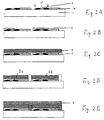
- a non-conductive passivation layer 3 which may comprise inorganic (e.g. SiO 2 ) and/or organic (e.g. a cured photoresist) non-conductive materials, is applied in such a way as to cover the source electrode or source region S and the gap or channel region C but to leave at least some part of the drain electrode or drain region D exposed.
- This layer 3 may be applied using standard lithographic techniques but may also be applied using other techniques such as shadow mask evaporation (see Fig. 1B).
- a matrix of cathodes 5, which can cover also the area covered by the TFTs and which define the area of the pixels in a display device according to the invention is applied, for example by vacuum evaporation or sputtering.
- the cathode layer 5 (see Fig. 1C) may comprise but is not limited to Al, Mg, Ca, Ba, Li, Ag, In or any alloys comprising two or more of these metals.
- a stable metal such as Al or alloys thereof is used, which is resistant to photolithographic processing.
- a cathode layer 5 may be structured into pixel elements 5a, 5b, ...
- an additional flattening layer or partial layer 4 may be applied to the pixels in such a way as to create a flat surface at the top of the cathode layer 5 and the pixel electrodes 5a, 5b, ..., respectively.
- This may for example be done by evaporation of further cathode material using for example a shadow mask or by spincoating of organic materials out of a solution.
- the flattening layer 4 may be applied using the same methods before deposition of the cathode layer 5 (see Fig. 1C and 1D).
- one or more composite active organic and/or polymeric layer(s) is (are) applied to the cathode material, i.e. on top of the pixel areas.
- the composition of the layer(s) 6 may include any of the types of materials known in the literature or referred to in the state of the art. Coating may be done by spincoating, doctor blading, transfer printing, curtain coating, slot-dye coating, or printing techniques such as screen printing (see Fig. 1E).
- a transparent high work function electrode e.g. an anode 7 such as described in the state of the art is deposited.
- the anode layer may be structured into the elements 7a, 7b, ... desired for a display using standard methods such as lithography and etching. Structuring of the anode is, however, optional and may not be necessary even for high resolution displays. Subsequently one or more active organic and/or polymeric layers 6' are applied to the structured anode layer elements 7a, 7b ..., respectively.
- composition of such polymeric layers may include any of the types of materials known in the literature or referred to in the description of the state of the art. Again, coating may be done by spincoating, doctor blading, transfer printing, curtain coating, slot-dye coating, or other printing techniques such as screen printing.
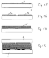
- the two coated substrates 1 to 6 and 8 to 6' are laminated together by application of heat and/or pressure as illustrated in Fig. 1K.
- the polymers have glass transition temperature or if it is a liquid crystalline polymer, it must have phase transition temperature from solid to liquid crystalline state or isotropic state, in which the viscosity of the polymer decreases. Above these appropriately selected temperatures the application of pressure can lead to good physical and electrical contact between the two polymer layers 6 and 6'. Therefore, the temperature of lamination should be higher than the glass transition temperature of at least one of the organic and/or polymeric layers.
- the device or display comprising such devices may be encapsulated if this is necessary or desired.
- a conventional TFT display substrate 1 such as used in the manufacture of liquid crystal displays is used as a substrate.
- Such substrates contain a matrix of TFTs 2 and of electrodes la usually made of ITO which define the pixel areas in such LCDs (see e.g. EP 0 845 770 A1).
- a non-conductive passivation layer 3 which covers the TFTs 2 but leaves part of the ITO electrodes la exposed.
- a matrix of cathodes i.e. in large pixel areas 5a, 5b, ... as above is deposited, which cover also the area containing the TFTs 2 and which in each case define the active area of a pixel in a device according to the invention.
- each pixel area is defined by the respective area 5a, 5b, ... of the cathode.
- the cathode electrode is the respective pixel electrode.
- the source electrode area S and the drain D of the TFT are c0overed by the non-conductive passivation layer 3 while the drain electrode is in contact with the respective cathode/ pixel electrode 5a, 5b.
- the pixel or cathode regions 5a, 5b, ... and/or the anode regions 7a, 7b, ... my be modified chemically before application of the organic and/or polymeric layer 6, 6' by absorption of functionalized dipoles.
- the functional groups which may be used to attach the dipoles may be, but are not limited to: Carboxylic acids Hydroxamine Thiols Phosphonates Sulfonates Amine.
- the molecules which are attached to the pixel regions 5a, 5b, ... and/or the anode regions 7a, 7b, ... in order to modify them may comprise in one especially preferred embodiment of the invention the same functional group for light emission and/or charge transport as the active organic or polymeric layer in the device which is adjacent to the thus modified electrode.
- the attached molecules comprise structures of the following formula R d - P - R a , where P is a ⁇ -conjugated system such as where R d is an electron donor group and R a is an electron acceptor group.
- Rd may be chosen from the following groups
- the attached molecules are of the form where either R att or R att 1 is an attachment group.
- the organic and/or polymeric material which is desired to be proximate to the modified electrode is applied.
- this may be done by spincoating, doctor blading, transfer printing, curtain coating, slot-dye coating, or other printing techniques such as screen printing.
- the modification of the electrodes 5a, 5b, ... and 7a, 7b, ... particularly the replacement of the usually unstable cathode by a stable electrode material like Al or an Al alloy, provides the possibility of manufacturing stable and efficient display devices, in comparison to the state of the art, forcing one to choose between stable cathode materials and high electron injection efficiency. Therefore, it will be possible in the future to prepare highly efficient organic light-emitting devices and displays using materials which are less stringent in their requirements for encapsulation and which are compatible with standard lithographic techniques for preparing structures.
- the process of a separate lamination furthermore allows for the TFTs necessary for high resolution displays to be deposited before the preparation of the light emitting element and on the non-transparent side of the display device, thus enabling a display with a higher aperture ratio than is possible with the state of the art.
- the panel is photo resist coated and processed by a usual photolithographic process and dry etched with oxygen at a pressure of 10 -3 torr only at data and gate line areas. The etching rate is 100 nm/min.
- (poly)octylfluorene of a molecular weight of 4000 dissolved in p-xylene at a concentration of ca. 20 mg/ml is spin coated onto the thus prepared substrate.
- the spin coater condition is 100 rpm for 4 seconds and then 3000 rpm for 30 seconds to obtain a 70 nm thick film 6 on the Al electrode (cathode 5a, 5b, ... in Fig. 1D) of the TFT panel.
- a 70 nm layer 6' of poly(octylfluorene) is deposited as above, is set on a previously applied polyfluorene film.
- the TFT panel (Fig. 1E) is placed on a hot plate which is set at 180 °C and kept at this temperature for 3 min.
- the second substrate (Fig. 1H) is applied to the first so that the two polymer layers 6, 6' are in face-to face contact with each other and heating is continued for another 3 min.
- a weight of 1 kg is applied on the combined panel under maintenance of the same temperature (see Fig. 1K).
- the glass edges of the laminated device are encapsulated with epoxy resin to keep out water and oxygen.
- a TFT/LEP display with 513000 pixels and a diagonal size of 1.35" (3,43 cm) which can have a brightness of 10 Cd/m 2 and the driving voltages are below 15 V.
- a display device is prepared as in Example 1 with the following modifications (see Figs. 3A to 3K):
- the panel is dipped into a breaker 10 (Fig. 3D 1 ) containing a 5 mg/ml solution in a mixture of acetonitrile and ethyl alcohol of the following composition for 5 minutes:
- the panel is rinsed in ethanol and dried under air at 50 °C for 5 min before deposition of the polymer layer 6.
- the rest of the preparation is as described in Example 1.
- Example 2 With the process of Example 2 and the structure described above, a TFT-LEP display with 513000 pixels and a diagonal size of 1.35" (3,43 cm) is obtained with a brightness of about 50 Cd/m 2 and with driving voltages below 15 V.
- a device is prepared as in Example 1 with the following differences (see Figs. 4A to 4K).
- the etching of the Al electrode e.g. cathode pixels 5a, 5b, ...;
- the deposition of the layer 6 of poly(octylfluorene) the panel is dipped into a breaker 10 containing a 5 mg/ml solution in a mixture of acetonitrile and ethyl alcohol of the following chemical composition for 5 min:
- the panel is rinsed in ethanol and dried under air at 50 °C for 5 min before deposition of the polymer layer 6.
- the second substrate is dipped into a breaker 11 containing a 5 mg/ml solution in a mixture of acetonitrile and ethanol of the following chemical composition for 5 min (Fig. 4D 1 ):
- the panel is rinsed in ethanol and dried under air at 50 °C for 5 min before deposition of the polymer layer 8.
- the rest of the preparation is as described in Example 1.
- TFT/LEP display with 513000 pixels and a diagonal size of 1.35" (3,43 cm) is obtained having a brightness of 100 Cd/m 2 and driving voltages below 12 V.
Landscapes
- Engineering & Computer Science (AREA)
- Microelectronics & Electronic Packaging (AREA)
- Physics & Mathematics (AREA)
- Optics & Photonics (AREA)
- Manufacturing & Machinery (AREA)
- Electroluminescent Light Sources (AREA)
- Devices For Indicating Variable Information By Combining Individual Elements (AREA)
- Thin Film Transistor (AREA)
Priority Applications (6)
| Application Number | Priority Date | Filing Date | Title |
|---|---|---|---|
| EP98119323A EP0996176B8 (fr) | 1998-10-13 | 1998-10-13 | Méthode de fabrication d'un dispositif d'affichage émetteur de lumière à matrice active |
| DE69831243T DE69831243T2 (de) | 1998-10-13 | 1998-10-13 | Herstellungsverfahren einer Licht emittierenden Anzeigevorrichtung mit aktiver Matrix |
| US09/415,807 US6461885B1 (en) | 1998-10-13 | 1999-10-11 | Method of fabricating and structure of an active matrix light-emitting display device |
| KR1019990043978A KR100608467B1 (ko) | 1998-10-13 | 1999-10-12 | 능동 매트릭스 발광 디스플레이 장치의 구조 및 제조 방법 |
| JP29158799A JP4536184B2 (ja) | 1998-10-13 | 1999-10-13 | アクティブマトリクス方式表示装置 |
| US10/216,130 US20030013220A1 (en) | 1998-10-13 | 2002-08-09 | Method of fabricating and structure of an active matrix light-emitting display device |
Applications Claiming Priority (1)
| Application Number | Priority Date | Filing Date | Title |
|---|---|---|---|
| EP98119323A EP0996176B8 (fr) | 1998-10-13 | 1998-10-13 | Méthode de fabrication d'un dispositif d'affichage émetteur de lumière à matrice active |
Publications (3)
| Publication Number | Publication Date |
|---|---|
| EP0996176A1 true EP0996176A1 (fr) | 2000-04-26 |
| EP0996176B1 EP0996176B1 (fr) | 2005-08-17 |
| EP0996176B8 EP0996176B8 (fr) | 2005-10-19 |
Family
ID=8232785
Family Applications (1)
| Application Number | Title | Priority Date | Filing Date |
|---|---|---|---|
| EP98119323A Expired - Lifetime EP0996176B8 (fr) | 1998-10-13 | 1998-10-13 | Méthode de fabrication d'un dispositif d'affichage émetteur de lumière à matrice active |
Country Status (5)
| Country | Link |
|---|---|
| US (2) | US6461885B1 (fr) |
| EP (1) | EP0996176B8 (fr) |
| JP (1) | JP4536184B2 (fr) |
| KR (1) | KR100608467B1 (fr) |
| DE (1) | DE69831243T2 (fr) |
Cited By (4)
| Publication number | Priority date | Publication date | Assignee | Title |
|---|---|---|---|---|
| WO2006112537A1 (fr) * | 2005-04-18 | 2006-10-26 | Seiko Epson Corporation | Procede de fabrication d’un element semi-conducteur, element semiconducteur, dispositif electronique et equipement electronique |
| EP1423991A4 (fr) * | 2001-07-27 | 2009-06-17 | Univ Ohio State | Procedes de production par stratification de dispositifs electroluminescents polymeres |
| EP1756886B1 (fr) * | 2004-06-02 | 2013-02-27 | Thomson Licensing | Diode organique electroluminescente comprenant une couche organique dopee |
| TWI492935B (zh) * | 2013-11-19 | 2015-07-21 | 國立清華大學 | 共軛芳香族化合物及其有機發光二極體 |
Families Citing this family (33)
| Publication number | Priority date | Publication date | Assignee | Title |
|---|---|---|---|---|
| TW480722B (en) * | 1999-10-12 | 2002-03-21 | Semiconductor Energy Lab | Manufacturing method of electro-optical device |
| TW471011B (en) | 1999-10-13 | 2002-01-01 | Semiconductor Energy Lab | Thin film forming apparatus |
| US6566808B1 (en) * | 1999-12-22 | 2003-05-20 | General Electric Company | Luminescent display and method of making |
| KR20020031202A (ko) * | 2000-10-23 | 2002-05-01 | 구본준, 론 위라하디락사 | 투명도가 낮은 기판을 이용한 평판 표시 장치 |
| JP3902938B2 (ja) * | 2000-10-31 | 2007-04-11 | キヤノン株式会社 | 有機発光素子の製造方法及び有機発光表示体の製造方法、有機発光素子及び有機発光表示体 |
| JP2002329576A (ja) * | 2001-04-27 | 2002-11-15 | Semiconductor Energy Lab Co Ltd | 発光装置およびその作製方法 |
| US20030016196A1 (en) * | 2001-07-17 | 2003-01-23 | Display Research Laboratories, Inc. | Thin film transistors suitable for use in flat panel displays |
| JP4176400B2 (ja) * | 2001-09-06 | 2008-11-05 | シャープ株式会社 | 表示装置 |
| US7248235B2 (en) | 2001-09-14 | 2007-07-24 | Sharp Kabushiki Kaisha | Display, method of manufacturing the same, and method of driving the same |
| DE10151440C1 (de) * | 2001-10-18 | 2003-02-06 | Siemens Ag | Organisches Elektronikbauteil, Verfahren zu seiner Herstellung und seine Verwendung |
| JP2003223992A (ja) * | 2002-01-31 | 2003-08-08 | Toyota Industries Corp | 有機elカラー表示装置 |
| KR101003624B1 (ko) * | 2002-03-26 | 2010-12-23 | 다이니폰 인사츠 가부시키가이샤 | 유기반도체 재료, 유기반도체 구조물 및, 유기반도체 장치 |
| KR100474000B1 (ko) * | 2002-08-13 | 2005-03-10 | 엘지.필립스 엘시디 주식회사 | 듀얼패널타입 유기전계발광 소자 및 그의 제조방법 |
| JP2004134279A (ja) * | 2002-10-11 | 2004-04-30 | Tohoku Pioneer Corp | 有機el表示パネル及びその製造方法 |
| US7063994B2 (en) * | 2003-07-11 | 2006-06-20 | Organic Vision Inc. | Organic semiconductor devices and methods of fabrication including forming two parts with polymerisable groups and bonding the parts |
| US20070178710A1 (en) * | 2003-08-18 | 2007-08-02 | 3M Innovative Properties Company | Method for sealing thin film transistors |
| US6844215B1 (en) * | 2003-08-25 | 2005-01-18 | Eastman Kodak Company | Method of forming tapered drain-to-anode connectors in a back plane for an active matrix OLED device |
| JP4727978B2 (ja) * | 2004-07-20 | 2011-07-20 | シャープ株式会社 | 有機デバイス及び有機エレクトロルミネッセンスデバイス |
| KR100647660B1 (ko) * | 2004-11-19 | 2006-11-23 | 삼성에스디아이 주식회사 | 박막 트랜지스터 및 이를 채용한 평판표시장치 |
| DE102005017655B4 (de) | 2005-04-15 | 2008-12-11 | Polyic Gmbh & Co. Kg | Mehrschichtiger Verbundkörper mit elektronischer Funktion |
| DE102005031448A1 (de) | 2005-07-04 | 2007-01-11 | Polyic Gmbh & Co. Kg | Aktivierbare optische Schicht |
| DE102005035589A1 (de) | 2005-07-29 | 2007-02-01 | Polyic Gmbh & Co. Kg | Verfahren zur Herstellung eines elektronischen Bauelements |
| DE102005044306A1 (de) | 2005-09-16 | 2007-03-22 | Polyic Gmbh & Co. Kg | Elektronische Schaltung und Verfahren zur Herstellung einer solchen |
| TW200809739A (en) * | 2006-08-08 | 2008-02-16 | Ritdisplay Corp | Method for fabricating active matrix organic electro-luminescence display panel |
| US7755156B2 (en) * | 2007-12-18 | 2010-07-13 | Palo Alto Research Center Incorporated | Producing layered structures with lamination |
| TWI425695B (zh) * | 2008-12-24 | 2014-02-01 | 國立清華大學 | 高分子薄膜及其製造方法暨包含該高分子薄膜的光電元件及其製造方法 |
| CN102674669B (zh) * | 2011-03-16 | 2014-12-03 | 京东方科技集团股份有限公司 | 一种玻璃基板的固定方法 |
| JP2014067522A (ja) * | 2012-09-25 | 2014-04-17 | Toshiba Corp | 表示装置およびその製造方法 |
| TWI543361B (zh) * | 2015-04-30 | 2016-07-21 | 友達光電股份有限公司 | 顯示面板之畫素單元及其製作方法 |
| KR102322084B1 (ko) * | 2015-04-30 | 2021-11-04 | 삼성디스플레이 주식회사 | 터치 센서 장치 및 그 제조 방법 |
| JP6685122B2 (ja) * | 2015-12-16 | 2020-04-22 | 住友化学株式会社 | 有機el素子の製造方法及び有機el素子 |
| CN106450015B (zh) * | 2016-10-11 | 2018-07-10 | 武汉华星光电技术有限公司 | 透明oled显示器及其制作方法 |
| CN111162189A (zh) * | 2018-11-07 | 2020-05-15 | 广东聚华印刷显示技术有限公司 | 发光器件及其制备方法和掩膜版 |
Citations (5)
| Publication number | Priority date | Publication date | Assignee | Title |
|---|---|---|---|---|
| JPH06220442A (ja) * | 1993-01-29 | 1994-08-09 | Toyo Ink Mfg Co Ltd | 有機エレクトロルミネッセンス素子 |
| WO1996033593A1 (fr) * | 1995-04-18 | 1996-10-24 | Cambridge Display Technology Limited | Fabrication de dispositifs organiques emettant de la lumiere |
| EP0777281A2 (fr) * | 1995-11-30 | 1997-06-04 | Motorola, Inc. | Passivation de dispositifs organiques électroluminescents |
| WO1998007202A1 (fr) * | 1996-08-08 | 1998-02-19 | International Business Machines Corporation | Cathodes en nitrure de gallium pour dispositifs electroluminescents et ecrans de visualisation |
| EP0845812A2 (fr) * | 1996-11-28 | 1998-06-03 | Casio Computer Co., Ltd. | Dispositif d'affichage |
Family Cites Families (11)
| Publication number | Priority date | Publication date | Assignee | Title |
|---|---|---|---|---|
| US5206749A (en) * | 1990-12-31 | 1993-04-27 | Kopin Corporation | Liquid crystal display having essentially single crystal transistors pixels and driving circuits |
| JP3170925B2 (ja) * | 1993-01-29 | 2001-05-28 | 東洋インキ製造株式会社 | 有機エレクトロルミネッセンス素子 |
| US5677545A (en) * | 1994-09-12 | 1997-10-14 | Motorola | Organic light emitting diodes with molecular alignment and method of fabrication |
| US5747928A (en) * | 1994-10-07 | 1998-05-05 | Iowa State University Research Foundation, Inc. | Flexible panel display having thin film transistors driving polymer light-emitting diodes |
| US5550066A (en) * | 1994-12-14 | 1996-08-27 | Eastman Kodak Company | Method of fabricating a TFT-EL pixel |
| JP2755216B2 (ja) * | 1995-06-20 | 1998-05-20 | 日本電気株式会社 | 有機薄膜el素子の製造方法 |
| US5737041A (en) * | 1995-07-31 | 1998-04-07 | Image Quest Technologies, Inc. | TFT, method of making and matrix displays incorporating the TFT |
| JP3457819B2 (ja) * | 1996-11-28 | 2003-10-20 | カシオ計算機株式会社 | 表示装置 |
| US5937272A (en) * | 1997-06-06 | 1999-08-10 | Eastman Kodak Company | Patterned organic layers in a full-color organic electroluminescent display array on a thin film transistor array substrate |
| GB9806066D0 (en) * | 1998-03-20 | 1998-05-20 | Cambridge Display Tech Ltd | Multilayer photovoltaic or photoconductive devices |
| US6312836B1 (en) * | 1998-04-10 | 2001-11-06 | The Trustees Of Princeton University | Color-tunable organic light emitting devices |
-
1998
- 1998-10-13 DE DE69831243T patent/DE69831243T2/de not_active Expired - Lifetime
- 1998-10-13 EP EP98119323A patent/EP0996176B8/fr not_active Expired - Lifetime
-
1999
- 1999-10-11 US US09/415,807 patent/US6461885B1/en not_active Expired - Lifetime
- 1999-10-12 KR KR1019990043978A patent/KR100608467B1/ko not_active Expired - Fee Related
- 1999-10-13 JP JP29158799A patent/JP4536184B2/ja not_active Expired - Fee Related
-
2002
- 2002-08-09 US US10/216,130 patent/US20030013220A1/en not_active Abandoned
Patent Citations (5)
| Publication number | Priority date | Publication date | Assignee | Title |
|---|---|---|---|---|
| JPH06220442A (ja) * | 1993-01-29 | 1994-08-09 | Toyo Ink Mfg Co Ltd | 有機エレクトロルミネッセンス素子 |
| WO1996033593A1 (fr) * | 1995-04-18 | 1996-10-24 | Cambridge Display Technology Limited | Fabrication de dispositifs organiques emettant de la lumiere |
| EP0777281A2 (fr) * | 1995-11-30 | 1997-06-04 | Motorola, Inc. | Passivation de dispositifs organiques électroluminescents |
| WO1998007202A1 (fr) * | 1996-08-08 | 1998-02-19 | International Business Machines Corporation | Cathodes en nitrure de gallium pour dispositifs electroluminescents et ecrans de visualisation |
| EP0845812A2 (fr) * | 1996-11-28 | 1998-06-03 | Casio Computer Co., Ltd. | Dispositif d'affichage |
Non-Patent Citations (4)
| Title |
|---|
| CABRERA ET AL.: "Blue transparent Langmuir Blodgett films for second harmonic generation", NONLINEAR OPTICS, vol. 9, 1995, pages 161 - 169, XP002095803 * |
| CHAYANOV B A ET AL: "PROTECTION OF ORGANIC THIN-FILM LIGHT-EMITTING DIODES", TECHNICAL PHYSICS LETTERS, vol. 23, no. 3, March 1997 (1997-03-01), pages 207, XP000619731 * |
| DATABASE WPI Section Ch Week 9436, Derwent World Patents Index; Class E19, AN 94-291165, XP002095804 * |
| NUESCH F ET AL: "DIRIVATIZED ELECTRODES IN THE CONSTRUCTION OF ORGANIC LIGHT EMITTING DIODES", ADVANCED MATERIALS, vol. 9, no. 3, February 1997 (1997-02-01), pages 222 - 225, XP000682002 * |
Cited By (5)
| Publication number | Priority date | Publication date | Assignee | Title |
|---|---|---|---|---|
| EP1423991A4 (fr) * | 2001-07-27 | 2009-06-17 | Univ Ohio State | Procedes de production par stratification de dispositifs electroluminescents polymeres |
| EP1756886B1 (fr) * | 2004-06-02 | 2013-02-27 | Thomson Licensing | Diode organique electroluminescente comprenant une couche organique dopee |
| WO2006112537A1 (fr) * | 2005-04-18 | 2006-10-26 | Seiko Epson Corporation | Procede de fabrication d’un element semi-conducteur, element semiconducteur, dispositif electronique et equipement electronique |
| US7683368B2 (en) | 2005-04-18 | 2010-03-23 | Seiko Epson Corporation | Method of manufacturing semiconductor element, semiconductor element, electronic device, and electronic equipment |
| TWI492935B (zh) * | 2013-11-19 | 2015-07-21 | 國立清華大學 | 共軛芳香族化合物及其有機發光二極體 |
Also Published As
| Publication number | Publication date |
|---|---|
| KR100608467B1 (ko) | 2006-08-09 |
| KR20000028999A (ko) | 2000-05-25 |
| JP2000173770A (ja) | 2000-06-23 |
| EP0996176B1 (fr) | 2005-08-17 |
| US20030013220A1 (en) | 2003-01-16 |
| US6461885B1 (en) | 2002-10-08 |
| DE69831243T2 (de) | 2006-08-10 |
| EP0996176B8 (fr) | 2005-10-19 |
| JP4536184B2 (ja) | 2010-09-01 |
| DE69831243D1 (de) | 2005-09-22 |
Similar Documents
| Publication | Publication Date | Title |
|---|---|---|
| EP0996176B1 (fr) | Méthode de fabrication d'un dispositif d'affichage émetteur de lumière à matrice active | |
| TWI248322B (en) | Organic electro luminescence device and fabrication method thereof | |
| US8253910B2 (en) | Display employing organic material | |
| TWI578542B (zh) | 包含薄膜電晶體的基板、製造該基板之方法以及包含該基板的有機發光顯示裝置 | |
| US7965034B2 (en) | Organic electroluminescence display device comprising a contact electrode with elasticity and fabricating method thereof | |
| JP2020178136A (ja) | 表示装置 | |
| US6879099B2 (en) | Organic EL element and organic EL display | |
| US8030842B2 (en) | Display device and method of making display device | |
| US7663147B2 (en) | Display apparatus and fabricating method thereof | |
| US20110198598A1 (en) | Organic light emitting display apparatus and method of manufacturing the same | |
| US20070057624A1 (en) | Patterns of electrically conducting polymers and their application as electrodes or electrical contacts | |
| US7897975B2 (en) | Light emitting display device and method for fabricating the same | |
| US7173378B2 (en) | Active matrix organic electroluminescent display device having organic thin-film transistor and method for manufacturing the display device | |
| EP0953213A2 (fr) | Motifs de polymeres electroconducteurs et leurs applications comme electrodes ou contacts electriques | |
| CN100508678C (zh) | 显示装置的制造方法 | |
| CN101393889A (zh) | 显示装置的制造方法 | |
| US20040017151A1 (en) | Organic electroluminescent display device and method of fabricating the same | |
| JP2004145244A (ja) | 表示装置 | |
| US20010009280A1 (en) | Organic electroluminescence display device | |
| JP2012506568A (ja) | ディスプレイ駆動部 | |
| TWI320294B (en) | Organic semiconductor light-emitting element and display device | |
| JP2006049811A (ja) | 有機薄膜トランジスタ及びこれを備えたフラットパネルディスプレイ装置 | |
| JP2004152595A (ja) | 表示装置 | |
| CN109326632A (zh) | 显示面板及显示装置 | |
| US20110171760A1 (en) | Method for manufacturing thin film transistor and display device |
Legal Events
| Date | Code | Title | Description |
|---|---|---|---|
| PUAI | Public reference made under article 153(3) epc to a published international application that has entered the european phase |
Free format text: ORIGINAL CODE: 0009012 |
|
| AK | Designated contracting states |
Kind code of ref document: A1 Designated state(s): DE FR GB |
|
| AX | Request for extension of the european patent |
Free format text: AL;LT;LV;MK;RO;SI |
|
| RAP1 | Party data changed (applicant data changed or rights of an application transferred) |
Owner name: SONY INTERNATIONAL (EUROPE) GMBH |
|
| 17P | Request for examination filed |
Effective date: 20000929 |
|
| AKX | Designation fees paid |
Free format text: DE FR GB |
|
| 17Q | First examination report despatched |
Effective date: 20040322 |
|
| GRAP | Despatch of communication of intention to grant a patent |
Free format text: ORIGINAL CODE: EPIDOSNIGR1 |
|
| RTI1 | Title (correction) |
Free format text: METHOD OF FABRICATING AN ACTIVE MATRIX LIGHT-EMITTING DISPLAY DEVICE |
|
| GRAS | Grant fee paid |
Free format text: ORIGINAL CODE: EPIDOSNIGR3 |
|
| GRAA | (expected) grant |
Free format text: ORIGINAL CODE: 0009210 |
|
| AK | Designated contracting states |
Kind code of ref document: B1 Designated state(s): DE FR GB |
|
| REG | Reference to a national code |
Ref country code: GB Ref legal event code: FG4D |
|
| REF | Corresponds to: |
Ref document number: 69831243 Country of ref document: DE Date of ref document: 20050922 Kind code of ref document: P |
|
| RAP2 | Party data changed (patent owner data changed or rights of a patent transferred) |
Owner name: SONY DEUTSCHLAND GMBH |
|
| ET | Fr: translation filed | ||
| PLBE | No opposition filed within time limit |
Free format text: ORIGINAL CODE: 0009261 |
|
| STAA | Information on the status of an ep patent application or granted ep patent |
Free format text: STATUS: NO OPPOSITION FILED WITHIN TIME LIMIT |
|
| 26N | No opposition filed |
Effective date: 20060518 |
|
| REG | Reference to a national code |
Ref country code: DE Ref legal event code: R082 Ref document number: 69831243 Country of ref document: DE Representative=s name: DENNEMEYER & ASSOCIATES S.A., LU Ref country code: DE Ref legal event code: R082 Ref document number: 69831243 Country of ref document: DE Representative=s name: MUELLER HOFFMANN & PARTNER PATENTANWAELTE MBB, DE Ref country code: DE Ref legal event code: R081 Ref document number: 69831243 Country of ref document: DE Owner name: JOLED INC., JP Free format text: FORMER OWNER: SONY DEUTSCHLAND GMBH, 50829 KOELN, DE Ref country code: DE Ref legal event code: R081 Ref document number: 69831243 Country of ref document: DE Owner name: SONY CORPORATION, JP Free format text: FORMER OWNER: SONY DEUTSCHLAND GMBH, 50829 KOELN, DE |
|
| REG | Reference to a national code |
Ref country code: GB Ref legal event code: 732E Free format text: REGISTERED BETWEEN 20150618 AND 20150624 |
|
| REG | Reference to a national code |
Ref country code: FR Ref legal event code: PLFP Year of fee payment: 18 |
|
| REG | Reference to a national code |
Ref country code: DE Ref legal event code: R082 Ref document number: 69831243 Country of ref document: DE Representative=s name: DENNEMEYER & ASSOCIATES S.A., LU Ref country code: DE Ref legal event code: R081 Ref document number: 69831243 Country of ref document: DE Owner name: JOLED INC., JP Free format text: FORMER OWNER: SONY CORPORATION, TOKYO, JP |
|
| PGFP | Annual fee paid to national office [announced via postgrant information from national office to epo] |
Ref country code: GB Payment date: 20151021 Year of fee payment: 18 Ref country code: DE Payment date: 20151022 Year of fee payment: 18 |
|
| REG | Reference to a national code |
Ref country code: FR Ref legal event code: TP Owner name: SONY CORPORATION, JP Effective date: 20160111 |
|
| PGFP | Annual fee paid to national office [announced via postgrant information from national office to epo] |
Ref country code: FR Payment date: 20151023 Year of fee payment: 18 |
|
| REG | Reference to a national code |
Ref country code: GB Ref legal event code: 732E Free format text: REGISTERED BETWEEN 20160204 AND 20160210 |
|
| REG | Reference to a national code |
Ref country code: FR Ref legal event code: TP Owner name: JOLED INC., JP Effective date: 20160405 |
|
| REG | Reference to a national code |
Ref country code: DE Ref legal event code: R119 Ref document number: 69831243 Country of ref document: DE |
|
| GBPC | Gb: european patent ceased through non-payment of renewal fee |
Effective date: 20161013 |
|
| REG | Reference to a national code |
Ref country code: FR Ref legal event code: ST Effective date: 20170630 |
|
| PG25 | Lapsed in a contracting state [announced via postgrant information from national office to epo] |
Ref country code: FR Free format text: LAPSE BECAUSE OF NON-PAYMENT OF DUE FEES Effective date: 20161102 Ref country code: DE Free format text: LAPSE BECAUSE OF NON-PAYMENT OF DUE FEES Effective date: 20170503 Ref country code: GB Free format text: LAPSE BECAUSE OF NON-PAYMENT OF DUE FEES Effective date: 20161013 |