EP0996189A2 - Wandler für dielektrische Leitung, dielektrische Leitungseinheit, Richtkoppler, Hochfrequenzschaltungsmodul, und Sender-Empfänger - Google Patents
Wandler für dielektrische Leitung, dielektrische Leitungseinheit, Richtkoppler, Hochfrequenzschaltungsmodul, und Sender-Empfänger Download PDFInfo
- Publication number
- EP0996189A2 EP0996189A2 EP99119642A EP99119642A EP0996189A2 EP 0996189 A2 EP0996189 A2 EP 0996189A2 EP 99119642 A EP99119642 A EP 99119642A EP 99119642 A EP99119642 A EP 99119642A EP 0996189 A2 EP0996189 A2 EP 0996189A2
- Authority
- EP
- European Patent Office
- Prior art keywords
- dielectric
- line
- dielectric line
- stripline
- converter
- Prior art date
- Legal status (The legal status is an assumption and is not a legal conclusion. Google has not performed a legal analysis and makes no representation as to the accuracy of the status listed.)
- Withdrawn
Links
- 239000004020 conductor Substances 0.000 claims abstract description 83
- 230000005540 biological transmission Effects 0.000 claims description 6
- 230000001902 propagating effect Effects 0.000 claims description 3
- 238000006243 chemical reaction Methods 0.000 abstract description 42
- 238000010276 construction Methods 0.000 description 33
- 238000010586 diagram Methods 0.000 description 6
- 238000000034 method Methods 0.000 description 4
- 238000005259 measurement Methods 0.000 description 3
- 230000000644 propagated effect Effects 0.000 description 3
- 239000000919 ceramic Substances 0.000 description 2
- 239000002131 composite material Substances 0.000 description 2
- 229920003002 synthetic resin Polymers 0.000 description 2
- 239000000057 synthetic resin Substances 0.000 description 2
- 241000490025 Schefflera digitata Species 0.000 description 1
- 230000006866 deterioration Effects 0.000 description 1
- 230000002542 deteriorative effect Effects 0.000 description 1
- 239000003989 dielectric material Substances 0.000 description 1
- 238000001746 injection moulding Methods 0.000 description 1
- 235000015250 liver sausages Nutrition 0.000 description 1
- 239000000463 material Substances 0.000 description 1
- 239000002184 metal Substances 0.000 description 1
- 239000004810 polytetrafluoroethylene Substances 0.000 description 1
- 229920001343 polytetrafluoroethylene Polymers 0.000 description 1
- 238000004088 simulation Methods 0.000 description 1
Images


Classifications
-
- H—ELECTRICITY
- H01—ELECTRIC ELEMENTS
- H01P—WAVEGUIDES; RESONATORS, LINES, OR OTHER DEVICES OF THE WAVEGUIDE TYPE
- H01P3/00—Waveguides; Transmission lines of the waveguide type
- H01P3/16—Dielectric waveguides, i.e. without a longitudinal conductor
- H01P3/165—Non-radiating dielectric waveguides
-
- H—ELECTRICITY
- H01—ELECTRIC ELEMENTS
- H01P—WAVEGUIDES; RESONATORS, LINES, OR OTHER DEVICES OF THE WAVEGUIDE TYPE
- H01P5/00—Coupling devices of the waveguide type
- H01P5/08—Coupling devices of the waveguide type for linking dissimilar lines or devices
- H01P5/087—Transitions to a dielectric waveguide
-
- H—ELECTRICITY
- H01—ELECTRIC ELEMENTS
- H01P—WAVEGUIDES; RESONATORS, LINES, OR OTHER DEVICES OF THE WAVEGUIDE TYPE
- H01P5/00—Coupling devices of the waveguide type
- H01P5/12—Coupling devices having more than two ports
- H01P5/16—Conjugate devices, i.e. devices having at least one port decoupled from one other port
- H01P5/18—Conjugate devices, i.e. devices having at least one port decoupled from one other port consisting of two coupled guides, e.g. directional couplers
Definitions
- the present invention relates to a line converter between dielectric lines of different kinds, and a directional coupler, dielectric line unit, high-frequency circuit module, and transmitter-receiver which use the line converter.
- a line converter between the waveguide and dielectric line is required.
- a line converter between a line made up of a waveguide in which a dielectric material is loaded(filled) (hereinafter, called DWG) and a non-radiative dielectric line in which a dielectric stripline is arranged between parallel conductor surfaces (hereinafter, called NRD guide) is shown in Japanese Unexamined Patent Publication No. 8-70209.
- DWG dielectric material is loaded(filled)
- NRD guide non-radiative dielectric line in which a dielectric stripline is arranged between parallel conductor surfaces
- a directional coupler of a parallel-wire line type in which two dielectric striplines are arranged in parallel between two upper and lower conductor surfaces is used.
- An NRD guide can be used as a dielectric line, but the frequency bandwidth in which the characteristic values of power distribution ratio, and so on, are kept within fixed values is narrow.
- a directional coupler of a waveguide type is composed of a DWG, although broad-band characteristics can be obtained, a line converter between the above DWG and NRD guide is required with a directional coupler of the DWG in order to realize the NRD guide as an input-output. As the result, the whole system becomes large-sized.
- a line converter comprises a first-kind dielectric line having upper and lower surfaces as a conductor surface of a dielectric stripline and spaces beside the dielectric stripline, a second-kind dielectric line having upper and lower surfaces and side surfaces as a conductor surface of a dielectric stripline, and a dielectric stripline connected to the dielectric striplines of the first-kind and second-kind dielectric line or being continuous with the dielectric striplines of the first-kind and second-kind dielectric line, wherein the space between the upper and lower conductor surfaces in the region except the dielectric striplines is made narrower than the space between the upper and lower conductor surfaces in the first-kind line, and wherein the space between the conductor surfaces in the second-kind dielectric line portion is made nearly zero.
- the line length between the first-kind dielectric line and the second-kind dielectric line is made an odd multiple of a fourth of a wavelength on the line, the reflected waves at the two locations in which the space between the upper and lower conductor surfaces sandwiching the dielectric stripline changes are superposed in opposite phase, and consequently the reflected waves are canceled. Accordingly, the reflection characteristic is improved.
- a line converter comprises a first-kind dielectric line having upper and lower surfaces as a conductor surface of a dielectric stripline and spaces beside the dielectric stripline, a second-kind dielectric line having upper and lower surfaces and side surfaces as a conductor surface of a dielectric stripline, and a dielectric stripline connected to the dielectric striplines of the first-kind and second-kind dielectric line or being continuous with the dielectric striplines of the first-kind and second-kind dielectric line, wherein the space from the dielectric stripline to the side conductor surface is made a fixed value which is narrower than the space from the dielectric stripline of the first-kind dielectric line to the side conductor surface.
- the dimension of the line converter does not have to be long in its length direction. As the result, a short line converter in its length direction can be obtained.
- the line is composed of a dielectric line propagating a single LSM mode (hereinafter, called hyper-NRD guide) by making the space between the conductor surfaces of the above first-kind dielectric line narrower than the height of the dielectric stripline of the first-kind dielectric line, a dielectric line circuit having a dielectric line and dielectric-loaded waveguide which hardly causes any loss accompanying a mode conversion at a bend can be easily constructed.
- hyper-NRD guide a dielectric line propagating a single LSM mode
- the above dielectric line converter constitutes a dielectric line unit.
- a dielectric line unit using the second-kind dielectric line can be constructed so that a first-kind dielectric line can be directly connected to the dielectric line unit.
- the above dielectric line converter constitutes a directional coupler.
- the two second-kind dielectric lines which are joined together or integrated constitute a directional coupler.
- a directional coupler into which input can be given through an NRD guide and which has a broad-band characteristic can be obtained.
- the above dielectric line unit or directional coupler to be used in the propagation portion of a transmission signal or reception signal constitutes a high-frequency circuit module.
- the above high-frequency circuit module, and a transmission circuit and reception circuit constitute a transmitter-receiver.
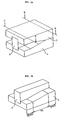
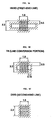
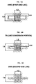
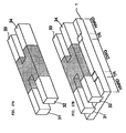
- Figs. 1 and 2 The construction of a dielectric line converter according to a first embodiment of the present invention is shown in Figs. 1 and 2.
- Fig. 1A is a perspective view of the whole of the main part
- Fig. 1B is a perspective view of Fig. 1A in which the upper conductor plate is removed.
- Fig. 2A is a sectional view taken on line A - A of Fig. 1A
- Fig. 1B is a sectional view taken on line B - B.
- reference numerals 1 and 2 represent a conductor plate which is composed of an electrode film formed on the surface of a molded insulating plate or a conductor plate which is composed of a processed metal plate, respectively.
- Reference numeral 3 represents a dielectric stripline produced by injection molding or cutting work, which is made up of synthetic resin, ceramics, or their composite materials. As shown in the figure, by arranging the dielectric stripline 3 between the upper and lower conductor plates 1 and 2, a first-kind dielectric line, a second-kind dielectric line, and a line conversion portion therebetween are constructed.
- the dimension in height and width direction of the dielectric stripline 3 is constant in any one of the first-kind dielectric line, second-kind dielectric line, and line conversion portion.
- the first-kind dielectric line portion the space h between the opposing surfaces (conductor surfaces) of the upper and lower conductor plates is made to be smaller than the height dimension of the dielectric stripline 3.
- a hyper-NRD guide (indicated by HNRD in the figure) propagating a single LSM01 mode is constructed.
- the second-kind dielectric line portion the upper and lower conductor plates 1 and 2 are put one on another, that is, the space between the opposing surfaces is made to be nearly zero.
- the groove depth in the conductor plates of the second-kind dielectric line portion is set to be half of the height dimension of the dielectric stripline 3.
- the second-kind dielectric line is made a dielectric-loaded waveguide (indicated by DWG in the figure).
- the groove depth is gradually changed so that the space between the opposing surfaces of the upper and lower conductor pates 1 and 2 becomes tapered over from the first-kind dielectric line portion to the second-kind dielectric line portion. Because of this construction, the reflection is reduced at the input-output portions or half-way, and a good reflection characteristic is maintained as a line converter.
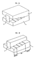
- Fig. 3 shows the construction of a dielectric line converter according to a second embodiment.
- the space between the opposing surfaces of the upper and lower conductor plates 1 and 2 of the line conversion portion is changed stepwise from the space in the first-kind dielectric line portion to the space (nearly zero) in the second-kind dielectric line portion.
- the space difference in the portion in which the space between the opposing surfaces of the upper and lower conductor plates 1 and 2 changes stepwise is small, the reflection is suppressed to be low, and the total reflection characteristic can be kept good.
- Fig. 4A is a perspective view of the whole of the main part
- Fig. 4B is a perspective view of Fig. 4A in which the upper conductor plate is removed.
- Reference numerals 1 and 2 represent a conductor plate
- reference numeral 3 represents a dielectric stripline.
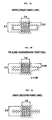
- Fig. 5A is a sectional view in the first-kind dielectric line portion
- Fig. 5B is a sectional view in the line conversion portion
- Fig. 5C is a sectional view in the second-kind dielectric line portion.
- the height and width of the dielectric stripline 3 are 2.2 mm and 1.8 mm, respectively, and are constant in any of the first-kind dielectric line, second-kind dielectric line, and line conversion portion.
- the groove depth given in the conductor plate of the first-kind dielectric line portion is made 0.5 mm
- the groove depth in the line conversion portion is 0.65 mm
- the groove depth in the second-kind dielectric line is 1.1 mm.
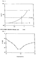
- the relationship of the characteristic impedance of the line to the space between the conductor surfaces of the upper and lower conductor plates 1 and 2 is shown in Fig. 6.
- Z1 represents the characteristic impedance of the first-kind dielectric line
- Z2 represents the characteristic impedance of the second-kind dielectric line.
- the space between the conductor surfaces is determined so that the characteristic impedance of the line conversion portion is given by ⁇ ( Z1 ⁇ Z2 )
- the impedance matching between the lines of the two kinds can be realized.
- the space between the conductor surfaces is 0.9 mm.
- the line length L of the line conversion portion is set to be ⁇ g/4 or an odd multiple of ⁇ g/4.
- the wavelength is in a 60 GHz band and L is 1.85 mm.
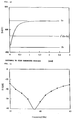
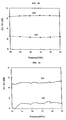
- Fig. 7 shows the reflection characteristic of a dielectric line converter constructed as in the above which is based on the three-dimensional finite element method. In this way, a low reflection characteristic of -30 dB can be obtained in a 60 GHz band.
- Fig. 8 is a perspective view of a dielectric line converter with the upper conductor plate removed.
- the space between the upper and lower conductor plates of a first-kind dielectric line portion is kept constant, and the space between the upper and lower conductor plates of a second-kind dielectric line is made nearly zero.
- the groove is expanded toward the side of a dielectric stripline 3, and the groove depth in that portion is made the same as the groove depth of the conductor plate in the first-kind dielectric line.
- Fig. 9A is a sectional view of the first-kind dielectric line portion
- Fig. 9B is a sectional view of the line conversion portion
- Fig. 9C is a sectional view of the second-kind dielectric line portion.
- the height and width of the dielectric line 3 are 2.2 mm and 1.8 mm, respectively, and are constant in any of the first-kind dielectric line, second-kind dielectric line, and line conversion portion.
- the groove depth given in the conductor plate of the first-kind dielectric line portion is made 0.5 mm.
- the groove depth in the line conversion portion is also 0.5 mm, but the space to the side conductor surface in the line conversion portion is made 0.16.
- the groove depth in the second-kind dielectric line is 1.1 mm.
- the relationship of the characteristic impedance of the line to the distance from the dielectric stripline to the side conductor surface is shown in Fig. 10.
- Z1 represents the characteristic impedance of the first-kind dielectric line
- Z2 represents the characteristic impedance of the second-kind dielectric line.
- the space from the dielectric stripline to the side conductor surface is determined so that the characteristic impedance of the line conversion portion is given by ⁇ ( Z1 ⁇ Z2 )
- the impedance matching between the lines of the two kinds can be realized.
- the space is 0.16 mm.
- the line length L of the line conversion portion is set to be ⁇ g/4 or an odd multiple of ⁇ g/4.
- the wavelength is in a 60 GHz band and L is 1.83 mm.
- Fig. 11 shows the reflection characteristic of a dielectric line converter constructed as in the above which is based on the three-dimensional finite element method. In this way, a low reflection characteristic of -30 dB can be obtained in a 60 GHz band.
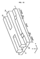
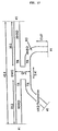
- Fig. 12 is a perspective view of a directional coupler with the upper conductor plate removed, and Fig. 13 is its top view.
- the portions indicated by 31, 32, 33, and 34 are dielectric striplines, and in the example they are integrally molded substantially in a H-shape. In the conductor plate 1 grooves in which the dielectric stripline 31 through 34 are fitted to a certain depth are formed.
- the upper conductor plate also has the same construction.
- the line conversion takes place in order of the first-kind dielectric line, line conversion portion, second-kind dielectric line, line conversion portion, and first-kind dielectric line.
- the line conversion takes place in order of the first-kind dielectric line, line conversion portion, second-kind dielectric line, line conversion portion, and first-kind dielectric line.
- the above dielectric striplines are integrated in a part of the portion constituting the second-kind dielectric line. Because of this, the second-kind dielectric line portion is made to function as a directional coupler of DWG.
- the directional coupler of DWG shows a broad-band characteristic just as the directional coupler using a cavity waveguide is broad-band.
- the four parts can be used as hyper-NRDs, when a directional coupler is given in a dielectric line circuit using a hyper-NRD guide, the whole of them can be made greatly small-sized.
- the space between the upper and lower conductor plates of the first-kind and second-kind dielectric line portion and the space between the upper and lower conductor plates of the line conversion portion are the same as in the example shown as the third embodiment in Fig. 5.
- the dimension and material of the dielectric striplines are the same as in the third embodiment.
- the dimension of each portion shown in Fig. 13 is the values of a directional coupler designed for a 60 GHz band, and they are expressed in a unit of mm.
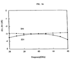
- Fig. 14 shows the distribution characteristic based on the three-dimensional finite element method.
- S31 and S41 characteristics are within -3 dB to result in an equal distribution characteristic, and, furthermore, the characteristic is maintained over a broad band.
- Fig. 15 is a top view of a directional coupler with the upper conductor plate removed.
- the directional coupler is basically the same as what is shown in Fig. 13, but the directional coupler to be used in a 76 GHz band is shown here.
- the line length of the TR conversion portion is made 1.3 mm and in the second-kind dielectric line portion the dimension of the portion to couple the parallel-wire lines is made smaller than shown in Fig. 13.
- Fig. 16 shows the sectional view of the line portions of the three kinds in the above directional coupler.
- Fig. 16A is a sectional view of the first-kind dielectric line portion
- Fig. 16B is a sectional view of the line conversion portion
- Fig. 16C is a sectional view of the second-kind dielectric line portion.
- the directional coupler is used in the higher frequency band, the dimension of each portion is made smaller than shown in Fig. 5.
- Fig. 17 shows the constriction of a directional coupler the characteristics of which were practically investigated, and is a top view of only the dielectric stripline portion.
- the power of the input signal from port No. 1 is distributed to No. 2 and No. 3.
- a hyper-NRD guide is entirely constituted outside the conversion portion TR, even if a bend of an arbitrary curvature is constructed, any loss accompanying mode conversion does scarcely occur.
- a bend having a radius of curvature of 5 mm (R5) is formed in order to lead out port No. 4 in a direction at a right angle to a straight line connecting port No.1 and port No. 3.
- Fig. 18 shows the result of the directional coupler shown in Fig. 15 which was simulated as no loss system using the three-dimensional finite element method.
- Fig. 19 is the result of an actual measurement of the directional coupler shown in Fig. 17. It is able to make the power distribution ratio nearly constant over such a broad frequency band.
- Fig. 20 is a top view of the module with the upper conductor plate removed
- Fig. 21 a block diagram of the above millimeter wave radar module.
- the millimeter wave radar module is principally made up of each unit of oscillator, isolator, directional coupler, circulator, and mixer.
- a millimeter wave signal is generated by a Gunn diode.
- the isolator is made up of a terminator connected to one port of the circulator which port three dielectric striplines as shown in the figure. That is, in the isolator, the millimeter wave signal from the oscillator is made propagated to the side of the directional coupler, and it is arranged that the reflected signal from the directional coupler is lead to the terminator.
- the directional coupler is of the same construction as that shown in Fig.
- a hyper-NRD guide to distribute an input signal from port No. 1 to port No. 3 and port No. 4 in a fixed power distribution ratio.
- the signal from port No. 3 is radiated as a TX signal toward a target from an antenna connected to an RF port through the circulator.
- the reflected signal from the target which the antenna received is input as an RX signal to the mixer through the circulator.
- a signal from port No. 4 of the directional coupler is input to the mixer as an LO signal, and the mixer mixes the RF signal and LO signal.
- an IF signal having a frequency component of f1 - f2 in accordance with the time difference caused by the path difference between two paths can be obtained.
- the distance to the target is measured.
- Fig. 22 is a top view with the upper conductor plate removed
- Fig. 23 is a block diagram of the above millimeter wave radar module.
- the millimeter wave radar module is principally made up of each unit of oscillator, isolator, directional coupler, circulator, up-converter, and down converter.
- a millimeter wave signal is generated by a Gunn diode.
- the isolator is made up of a terminator connected to one port of the circulator which port three dielectric striplines as shown in the figure, and in the isolator the millimeter wave signal from the oscillator is made propagated to the side of the directional coupler and it is arranged that the reflected signal from the directional coupler is lead to the terminator.
- the signal input from port No. 1 of the directional coupler is output from port No. 3 and port No.
- the up-converter mixes an LO signal from the directional coupler and an IF signal from an IF circuit, and outputs a signal containing a frequency signal of LO and IF to the circulator. This signal is radiated outside as a TX signal through the circulator.
- the signal is output to a waveguide through a WG converter to convert a hyper-NRD guide to a waveguide mode.
- the signal reflected from a target is input as an RX signal into the down converter through the circulator.
- the down converter mixes the LO signal oscillated in the oscillator and the RX signal and an IF signal containing an RX - LO component is obtained.
- Fig. 24 is a block diagram showing the construction of the whole of a transmitter-receiver according to a ninth embodiment, in which the above millimeter wave radar module is used.
- the RF circuit corresponds to the above millimeter wave radar module
- the IF circuit is made up of a filter circuit and AD converter for the IF signal obtained from the millimeter wave radar module.
- the signal processing circuit measures the distance from the antenna of the millimeter wave radar module to the target and calculates the relative speed by signal-processing or computing the digital data of the IF signal, and when required external circuits of mobile engine control units, and so on, are controlled.
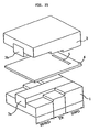
- a dielectric line unit according to a tenth embodiment is shown in Fig. 25.
- reference numerals 1 and 2 represent upper and lower conductor plates, and 3a and 3b represent divided upper and lower dielectric striplines.
- 4 represents a board in which a microstrip line 5, and so on, are formed, and the board sandwiched between the upper and lower conductor plates 1 and 2 constitutes a dielectric line unit.
- This dielectric line unit corresponds to a unit having the construction shown in Fig. 4 which is divided up and down at the middle portion and sandwiches the board therebetween.
- microstrip line 5 By the microstrip line 5 inserted in a DWG portion in a direction at a right angle to the line of the DWG, a line conversion between the DWG and microstrip line is performed. And generation of unwanted waves is reduced by such a line conversion between the DWG and microstrip line, compared with the case in which a direct line conversion between an NRD guide and microstrip line is carried out. More, a hollow portion is formed in the portion of the conductor plate 2 which is opposed to the microstrip line 5 so that the microstrip line 5 is not made in direct contact with the upper conductor plate 2.
- Fig. 26A is a perspective view of the whole of the main part
- Fig. 26B is a sectional view taken on line B - B of Fig. 26A
- Fig. 26C is a sectional view taken on line C - C of Fig. 26A.
- no groove is given in the upper and lower conductor plates 1 and 2 of the normal NRD guide in this example.
- the groove depth is gradually changed so that the space between the opposing surfaces of the upper and lower conductor plates 1 and 2 becomes tapered over from the normal NRD guide portion to the DWG portion.
- the conductor surface of a dielectric line was made up of the surface of a conductor plate.
- the conductor surface may be formed by metallizing a fixed portion of a dielectric stripline.
- a directional coupler the example is shown in Fig. 27.
- Fig. 27A is a perspective view of a dielectric stripline
- Fig. 27B is a perspective view of the directional coupler with the upper conductor plate removed.
- the portions indicated by 31, 32, 33, and 34 are dielectric lines, but different from the example shown in Fig. 12 an electrode film is formed on a dielectric stripline portion constituting the DWG. The construction of the others is the same as in Fig. 12.
- the metallized electrode functions as a conductor surface, and accordingly even if a more or less spacing is caused between the dielectric stripline and the conductor plate in the DWG portion a stable characteristic can be always realized.
- a line conversion is made without deterioration of reflection characteristics. Furthermore, as the line does not tend to be widened in its width direction, a dielectric line converter which is small-sized in its width direction can be obtained.
- the reflection at the discontinuity portion of the line over from a first-kind dielectric line to a second-kind dielectric line is more suppressed.
- reflected waves at two discontinuity portions are superposed in opposite phase, and as a result the reflected waves are canceled. Because of this the reflection characteristic is improved.
- a line converter which is short in its length direction can be obtained.
- a dielectric line circuit having an NRD guide and DWG which practically do not cause any loss accompanying the mode conversion in a bend can be easily constructed.
- a seventh aspect of the present invention when, for example, an element of a DWG is given to a dielectric line circuit, the element becomes possible to be directly connected in a dielectric line circuit of an NRD guide, and as a result it becomes possible to make the whole of small size.
- a small-sized high-frequency circuit module having broad-band characteristics in which the directional coupler or dielectric line unit is used in the propagation portion of a transmission signal or reception signal can be easily constructed.
- a small-sized transmitter-receiver having broad-band characteristics in which the high-frequency circuit module, transmission circuit, and reception circuit are given can be constructed.
Landscapes
- Waveguides (AREA)
- Microwave Amplifiers (AREA)
Applications Claiming Priority (2)
| Application Number | Priority Date | Filing Date | Title |
|---|---|---|---|
| JP30075498A JP3498597B2 (ja) | 1998-10-22 | 1998-10-22 | 誘電体線路変換構造、誘電体線路装置、方向性結合器、高周波回路モジュールおよび送受信装置 |
| JP30075498 | 1998-10-22 |
Publications (2)
| Publication Number | Publication Date |
|---|---|
| EP0996189A2 true EP0996189A2 (de) | 2000-04-26 |
| EP0996189A3 EP0996189A3 (de) | 2001-08-29 |
Family
ID=17888703
Family Applications (1)
| Application Number | Title | Priority Date | Filing Date |
|---|---|---|---|
| EP99119642A Withdrawn EP0996189A3 (de) | 1998-10-22 | 1999-10-04 | Wandler für dielektrische Leitung, dielektrische Leitungseinheit, Richtkoppler, Hochfrequenzschaltungsmodul, und Sender-Empfänger |
Country Status (5)
| Country | Link |
|---|---|
| US (1) | US6384694B1 (de) |
| EP (1) | EP0996189A3 (de) |
| JP (1) | JP3498597B2 (de) |
| CN (1) | CN1185756C (de) |
| CA (1) | CA2287036C (de) |
Cited By (15)
| Publication number | Priority date | Publication date | Assignee | Title |
|---|---|---|---|---|
| WO2005064740A1 (de) * | 2003-12-30 | 2005-07-14 | Robert Bosch Gmbh | Richtkoppler in streifenleitertechnik mit breitem koppelspalt |
| WO2014026089A1 (en) * | 2012-08-10 | 2014-02-13 | Waveconnex, Inc. | Dielectric coupling systems for ehf communications |
| US9197011B2 (en) | 2011-12-14 | 2015-11-24 | Keyssa, Inc. | Connectors providing haptic feedback |
| US9203597B2 (en) | 2012-03-02 | 2015-12-01 | Keyssa, Inc. | Systems and methods for duplex communication |
| US9322904B2 (en) | 2011-06-15 | 2016-04-26 | Keyssa, Inc. | Proximity sensing using EHF signals |
| US9374154B2 (en) | 2012-09-14 | 2016-06-21 | Keyssa, Inc. | Wireless connections with virtual hysteresis |
| US9379450B2 (en) | 2011-03-24 | 2016-06-28 | Keyssa, Inc. | Integrated circuit with electromagnetic communication |
| US9407311B2 (en) | 2011-10-21 | 2016-08-02 | Keyssa, Inc. | Contactless signal splicing using an extremely high frequency (EHF) communication link |
| US9426660B2 (en) | 2013-03-15 | 2016-08-23 | Keyssa, Inc. | EHF secure communication device |
| US9515859B2 (en) | 2011-05-31 | 2016-12-06 | Keyssa, Inc. | Delta modulated low-power EHF communication link |
| US9531425B2 (en) | 2012-12-17 | 2016-12-27 | Keyssa, Inc. | Modular electronics |
| US9553353B2 (en) | 2012-03-28 | 2017-01-24 | Keyssa, Inc. | Redirection of electromagnetic signals using substrate structures |
| US9553616B2 (en) | 2013-03-15 | 2017-01-24 | Keyssa, Inc. | Extremely high frequency communication chip |
| US9853696B2 (en) | 2008-12-23 | 2017-12-26 | Keyssa, Inc. | Tightly-coupled near-field communication-link connector-replacement chips |
| US10305196B2 (en) | 2012-04-17 | 2019-05-28 | Keyssa, Inc. | Dielectric lens structures for EHF radiation |
Families Citing this family (11)
| Publication number | Priority date | Publication date | Assignee | Title |
|---|---|---|---|---|
| JP3485054B2 (ja) | 1999-12-28 | 2004-01-13 | 株式会社村田製作所 | 異種非放射性誘電体線路変換部構造およびその装置 |
| JP2003218612A (ja) | 2001-11-16 | 2003-07-31 | Murata Mfg Co Ltd | 誘電体線路、高周波回路、および高周波回路装置 |
| JP3975978B2 (ja) * | 2002-08-27 | 2007-09-12 | 株式会社村田製作所 | 線路変換器、高周波モジュールおよび通信装置 |
| WO2005048314A2 (en) * | 2003-11-12 | 2005-05-26 | Silicon Pipe, Inc. | Tapered dielectric and conductor structures and applications thereof |
| US7466021B2 (en) * | 2003-11-17 | 2008-12-16 | Interconnect Portfolio, Llp | Memory packages having stair step interconnection layers |
| JP6104672B2 (ja) | 2013-03-29 | 2017-03-29 | モレックス エルエルシー | 高周波伝送装置 |
| US9692102B2 (en) * | 2015-09-25 | 2017-06-27 | Texas Instruments Incorporated | Dielectric waveguide socket for connecting a dielectric waveguide stub to a dielectric waveguide |
| US9490518B1 (en) * | 2015-09-28 | 2016-11-08 | Texas Instruments Incorporated | System for launching a signal into a dielectric waveguide |
| US10090602B2 (en) | 2016-12-21 | 2018-10-02 | Sierra Nevada Corporation | Waveguide feed for steerable beam antenna |
| JP7331717B2 (ja) * | 2020-01-29 | 2023-08-23 | 東京エレクトロン株式会社 | 方向性結合器、基板を処理する装置、及び基板を処理する方法 |
| CN113328227A (zh) * | 2021-05-27 | 2021-08-31 | 电子科技大学 | 一种微带线到非辐射介质波导的过渡结构 |
Citations (1)
| Publication number | Priority date | Publication date | Assignee | Title |
|---|---|---|---|---|
| GB763894A (en) * | 1954-01-14 | 1956-12-19 | Standard Telephones Cables Ltd | Radio frequency transmission system |
Family Cites Families (3)
| Publication number | Priority date | Publication date | Assignee | Title |
|---|---|---|---|---|
| JP3336733B2 (ja) | 1994-04-07 | 2002-10-21 | 株式会社村田製作所 | 移動手段用通信モジュール |
| JPH1065413A (ja) * | 1996-08-19 | 1998-03-06 | Murata Mfg Co Ltd | 誘電体線路型方向性結合器 |
| JP3498611B2 (ja) * | 1998-07-03 | 2004-02-16 | 株式会社村田製作所 | 方向性結合器、アンテナ装置および送受信装置 |
-
1998
- 1998-10-22 JP JP30075498A patent/JP3498597B2/ja not_active Expired - Fee Related
-
1999
- 1999-10-04 EP EP99119642A patent/EP0996189A3/de not_active Withdrawn
- 1999-10-20 CN CN99123346.8A patent/CN1185756C/zh not_active Expired - Fee Related
- 1999-10-21 US US09/425,841 patent/US6384694B1/en not_active Expired - Fee Related
- 1999-10-21 CA CA002287036A patent/CA2287036C/en not_active Expired - Fee Related
Patent Citations (1)
| Publication number | Priority date | Publication date | Assignee | Title |
|---|---|---|---|---|
| GB763894A (en) * | 1954-01-14 | 1956-12-19 | Standard Telephones Cables Ltd | Radio frequency transmission system |
Cited By (33)
| Publication number | Priority date | Publication date | Assignee | Title |
|---|---|---|---|---|
| WO2005064740A1 (de) * | 2003-12-30 | 2005-07-14 | Robert Bosch Gmbh | Richtkoppler in streifenleitertechnik mit breitem koppelspalt |
| US7525397B2 (en) | 2003-12-30 | 2009-04-28 | Robert Bosch Gmbh | Stripline directional coupler having a wide coupling gap |
| US9853696B2 (en) | 2008-12-23 | 2017-12-26 | Keyssa, Inc. | Tightly-coupled near-field communication-link connector-replacement chips |
| US10243621B2 (en) | 2008-12-23 | 2019-03-26 | Keyssa, Inc. | Tightly-coupled near-field communication-link connector-replacement chips |
| US10965347B2 (en) | 2008-12-23 | 2021-03-30 | Keyssa, Inc. | Tightly-coupled near-field communication-link connector-replacement chips |
| US9379450B2 (en) | 2011-03-24 | 2016-06-28 | Keyssa, Inc. | Integrated circuit with electromagnetic communication |
| US9444146B2 (en) | 2011-03-24 | 2016-09-13 | Keyssa, Inc. | Integrated circuit with electromagnetic communication |
| US9515859B2 (en) | 2011-05-31 | 2016-12-06 | Keyssa, Inc. | Delta modulated low-power EHF communication link |
| US9322904B2 (en) | 2011-06-15 | 2016-04-26 | Keyssa, Inc. | Proximity sensing using EHF signals |
| US9444523B2 (en) | 2011-06-15 | 2016-09-13 | Keyssa, Inc. | Proximity sensing using EHF signals |
| US9722667B2 (en) | 2011-06-15 | 2017-08-01 | Keyssa, Inc. | Proximity sensing using EHF signals |
| US9407311B2 (en) | 2011-10-21 | 2016-08-02 | Keyssa, Inc. | Contactless signal splicing using an extremely high frequency (EHF) communication link |
| US9647715B2 (en) | 2011-10-21 | 2017-05-09 | Keyssa, Inc. | Contactless signal splicing using an extremely high frequency (EHF) communication link |
| US9197011B2 (en) | 2011-12-14 | 2015-11-24 | Keyssa, Inc. | Connectors providing haptic feedback |
| US9203597B2 (en) | 2012-03-02 | 2015-12-01 | Keyssa, Inc. | Systems and methods for duplex communication |
| US9553353B2 (en) | 2012-03-28 | 2017-01-24 | Keyssa, Inc. | Redirection of electromagnetic signals using substrate structures |
| US10651559B2 (en) | 2012-03-28 | 2020-05-12 | Keyssa, Inc. | Redirection of electromagnetic signals using substrate structures |
| US10305196B2 (en) | 2012-04-17 | 2019-05-28 | Keyssa, Inc. | Dielectric lens structures for EHF radiation |
| US10069183B2 (en) | 2012-08-10 | 2018-09-04 | Keyssa, Inc. | Dielectric coupling systems for EHF communications |
| WO2014026089A1 (en) * | 2012-08-10 | 2014-02-13 | Waveconnex, Inc. | Dielectric coupling systems for ehf communications |
| US9515365B2 (en) | 2012-08-10 | 2016-12-06 | Keyssa, Inc. | Dielectric coupling systems for EHF communications |
| US9515707B2 (en) | 2012-09-14 | 2016-12-06 | Keyssa, Inc. | Wireless connections with virtual hysteresis |
| US9374154B2 (en) | 2012-09-14 | 2016-06-21 | Keyssa, Inc. | Wireless connections with virtual hysteresis |
| US10027382B2 (en) | 2012-09-14 | 2018-07-17 | Keyssa, Inc. | Wireless connections with virtual hysteresis |
| US10523278B2 (en) | 2012-12-17 | 2019-12-31 | Keyssa, Inc. | Modular electronics |
| US10033439B2 (en) | 2012-12-17 | 2018-07-24 | Keyssa, Inc. | Modular electronics |
| US9531425B2 (en) | 2012-12-17 | 2016-12-27 | Keyssa, Inc. | Modular electronics |
| US9960792B2 (en) | 2013-03-15 | 2018-05-01 | Keyssa, Inc. | Extremely high frequency communication chip |
| US9894524B2 (en) | 2013-03-15 | 2018-02-13 | Keyssa, Inc. | EHF secure communication device |
| US10602363B2 (en) | 2013-03-15 | 2020-03-24 | Keyssa, Inc. | EHF secure communication device |
| US9426660B2 (en) | 2013-03-15 | 2016-08-23 | Keyssa, Inc. | EHF secure communication device |
| US10925111B2 (en) | 2013-03-15 | 2021-02-16 | Keyssa, Inc. | EHF secure communication device |
| US9553616B2 (en) | 2013-03-15 | 2017-01-24 | Keyssa, Inc. | Extremely high frequency communication chip |
Also Published As
| Publication number | Publication date |
|---|---|
| JP3498597B2 (ja) | 2004-02-16 |
| CA2287036C (en) | 2003-02-11 |
| US6384694B1 (en) | 2002-05-07 |
| EP0996189A3 (de) | 2001-08-29 |
| CA2287036A1 (en) | 2000-04-22 |
| CN1257321A (zh) | 2000-06-21 |
| CN1185756C (zh) | 2005-01-19 |
| JP2000134008A (ja) | 2000-05-12 |
Similar Documents
| Publication | Publication Date | Title |
|---|---|---|
| EP0996189A2 (de) | Wandler für dielektrische Leitung, dielektrische Leitungseinheit, Richtkoppler, Hochfrequenzschaltungsmodul, und Sender-Empfänger | |
| US8089327B2 (en) | Waveguide to plural microstrip transition | |
| US5867120A (en) | Transmitter-receiver | |
| US5867073A (en) | Waveguide to transmission line transition | |
| JP2998614B2 (ja) | 誘電体線路 | |
| US6472961B1 (en) | Non-radiative dielectric line including convex or concave portion, and integrated circuit comprising the non-radiative dielectric line | |
| Zarifi et al. | A millimeter-wave six-port junction based on ridge gap waveguide | |
| CA2256283C (en) | Non radiative dielectric waveguide having a portion for line conversion between different types of non radiative dielectric waveguides | |
| EP0969545B1 (de) | Richtkoppler, Antennenanordnung, und Sender-Empfänger | |
| US6441698B1 (en) | Dielectric-waveguide attenuator, dielectric-waveguide terminator, and wireless apparatus incorporating same | |
| US6445355B2 (en) | Non-radiative hybrid dielectric line transition and apparatus incorporating the same | |
| KR100852377B1 (ko) | 소형 nrd 가이드벤드 | |
| US6931246B2 (en) | Line coupling structure, mixer, and receiving/transmitting apparatus comprised of suspended line and dielectric waveguide | |
| JP3846585B2 (ja) | 導波管ベンド、導波管プレートおよび高周波装置 | |
| US10665945B2 (en) | Millimeter-wave waveguide | |
| CN117559101A (zh) | 一种高隔离双波导探针功分/合成器 | |
| JP3617397B2 (ja) | 誘電体線路導波管変換器、誘電体線路接続構造、1次放射器、発振器および送信装置 | |
| JP2004120792A (ja) | 導波管変換構造、導波管接続構造、1次放射器、発振器および送信装置 | |
| JP3259637B2 (ja) | 送受信装置 | |
| JP2002532928A (ja) | 広帯域マイクロストリップから平行板導波管への転移部 | |
| Tan et al. | A Ku-band SIW six-port | |
| JPH1065413A (ja) | 誘電体線路型方向性結合器 | |
| JP2000134031A (ja) | アンテナ装置、およびそれを用いたアンテナ、送受信装置 | |
| EP4515625A1 (de) | Nicht-uniformierte anpassungs-ultrabreitbandduplexerstruktur | |
| JP2001044714A (ja) | 誘電体線路および無線装置 |
Legal Events
| Date | Code | Title | Description |
|---|---|---|---|
| PUAI | Public reference made under article 153(3) epc to a published international application that has entered the european phase |
Free format text: ORIGINAL CODE: 0009012 |
|
| 17P | Request for examination filed |
Effective date: 19991004 |
|
| AK | Designated contracting states |
Kind code of ref document: A2 Designated state(s): AT BE CH CY DE DK ES FI FR GB GR IE IT LI LU MC NL PT SE |
|
| AX | Request for extension of the european patent |
Free format text: AL;LT;LV;MK;RO;SI |
|
| PUAL | Search report despatched |
Free format text: ORIGINAL CODE: 0009013 |
|
| AK | Designated contracting states |
Kind code of ref document: A3 Designated state(s): AT BE CH CY DE DK ES FI FR GB GR IE IT LI LU MC NL PT SE |
|
| AX | Request for extension of the european patent |
Free format text: AL;LT;LV;MK;RO;SI |
|
| AKX | Designation fees paid |
Free format text: DE FR GB |
|
| 17Q | First examination report despatched |
Effective date: 20070820 |
|
| RAP1 | Party data changed (applicant data changed or rights of an application transferred) |
Owner name: MURATA MANUFACTURING CO., LTD. |
|
| GRAP | Despatch of communication of intention to grant a patent |
Free format text: ORIGINAL CODE: EPIDOSNIGR1 |
|
| STAA | Information on the status of an ep patent application or granted ep patent |
Free format text: STATUS: THE APPLICATION IS DEEMED TO BE WITHDRAWN |
|
| 18D | Application deemed to be withdrawn |
Effective date: 20091216 |