EP0997751A2 - Filtre optique passe-tout - Google Patents
Filtre optique passe-tout Download PDFInfo
- Publication number
- EP0997751A2 EP0997751A2 EP99308189A EP99308189A EP0997751A2 EP 0997751 A2 EP0997751 A2 EP 0997751A2 EP 99308189 A EP99308189 A EP 99308189A EP 99308189 A EP99308189 A EP 99308189A EP 0997751 A2 EP0997751 A2 EP 0997751A2
- Authority
- EP
- European Patent Office
- Prior art keywords
- optical
- pass
- filter
- optical filter
- pass optical
- Prior art date
- Legal status (The legal status is an assumption and is not a legal conclusion. Google has not performed a legal analysis and makes no representation as to the accuracy of the status listed.)
- Withdrawn
Links
- 230000003287 optical effect Effects 0.000 title claims abstract description 253
- 239000006185 dispersion Substances 0.000 claims abstract description 63
- 230000004044 response Effects 0.000 claims abstract description 30
- 238000004891 communication Methods 0.000 claims description 22
- 238000000034 method Methods 0.000 claims description 7
- 238000002310 reflectometry Methods 0.000 claims description 6
- 230000000737 periodic effect Effects 0.000 claims description 5
- 239000003989 dielectric material Substances 0.000 claims description 2
- 230000008878 coupling Effects 0.000 description 19
- 238000010168 coupling process Methods 0.000 description 19
- 238000005859 coupling reaction Methods 0.000 description 19
- 239000000835 fiber Substances 0.000 description 15
- 230000001419 dependent effect Effects 0.000 description 14
- 239000013307 optical fiber Substances 0.000 description 11
- 230000005540 biological transmission Effects 0.000 description 10
- 230000001934 delay Effects 0.000 description 7
- 238000013461 design Methods 0.000 description 6
- 230000007547 defect Effects 0.000 description 4
- 230000003595 spectral effect Effects 0.000 description 4
- 230000008859 change Effects 0.000 description 3
- 238000012937 correction Methods 0.000 description 3
- 238000012546 transfer Methods 0.000 description 3
- 230000003111 delayed effect Effects 0.000 description 2
- 230000000694 effects Effects 0.000 description 2
- 238000004519 manufacturing process Methods 0.000 description 2
- 238000005457 optimization Methods 0.000 description 2
- 239000000654 additive Substances 0.000 description 1
- 230000000996 additive effect Effects 0.000 description 1
- 230000003321 amplification Effects 0.000 description 1
- 230000007423 decrease Effects 0.000 description 1
- 239000000463 material Substances 0.000 description 1
- 238000003199 nucleic acid amplification method Methods 0.000 description 1
- 230000008569 process Effects 0.000 description 1
- 230000000644 propagated effect Effects 0.000 description 1
- 238000000926 separation method Methods 0.000 description 1
- 238000003860 storage Methods 0.000 description 1
Images


Classifications
-
- G—PHYSICS
- G02—OPTICS
- G02B—OPTICAL ELEMENTS, SYSTEMS OR APPARATUS
- G02B6/00—Light guides; Structural details of arrangements comprising light guides and other optical elements, e.g. couplings
- G02B6/24—Coupling light guides
- G02B6/26—Optical coupling means
- G02B6/28—Optical coupling means having data bus means, i.e. plural waveguides interconnected and providing an inherently bidirectional system by mixing and splitting signals
- G02B6/293—Optical coupling means having data bus means, i.e. plural waveguides interconnected and providing an inherently bidirectional system by mixing and splitting signals with wavelength selective means
- G02B6/29331—Optical coupling means having data bus means, i.e. plural waveguides interconnected and providing an inherently bidirectional system by mixing and splitting signals with wavelength selective means operating by evanescent wave coupling
- G02B6/29335—Evanescent coupling to a resonator cavity, i.e. between a waveguide mode and a resonant mode of the cavity
- G02B6/29338—Loop resonators
- G02B6/29343—Cascade of loop resonators
-
- B—PERFORMING OPERATIONS; TRANSPORTING
- B82—NANOTECHNOLOGY
- B82Y—SPECIFIC USES OR APPLICATIONS OF NANOSTRUCTURES; MEASUREMENT OR ANALYSIS OF NANOSTRUCTURES; MANUFACTURE OR TREATMENT OF NANOSTRUCTURES
- B82Y20/00—Nanooptics, e.g. quantum optics or photonic crystals
-
- G—PHYSICS
- G02—OPTICS
- G02B—OPTICAL ELEMENTS, SYSTEMS OR APPARATUS
- G02B6/00—Light guides; Structural details of arrangements comprising light guides and other optical elements, e.g. couplings
- G02B6/10—Light guides; Structural details of arrangements comprising light guides and other optical elements, e.g. couplings of the optical waveguide type
- G02B6/12—Light guides; Structural details of arrangements comprising light guides and other optical elements, e.g. couplings of the optical waveguide type of the integrated circuit kind
- G02B6/122—Basic optical elements, e.g. light-guiding paths
- G02B6/1225—Basic optical elements, e.g. light-guiding paths comprising photonic band-gap structures or photonic lattices
-
- G—PHYSICS
- G02—OPTICS
- G02B—OPTICAL ELEMENTS, SYSTEMS OR APPARATUS
- G02B6/00—Light guides; Structural details of arrangements comprising light guides and other optical elements, e.g. couplings
- G02B6/24—Coupling light guides
- G02B6/26—Optical coupling means
- G02B6/28—Optical coupling means having data bus means, i.e. plural waveguides interconnected and providing an inherently bidirectional system by mixing and splitting signals
- G02B6/293—Optical coupling means having data bus means, i.e. plural waveguides interconnected and providing an inherently bidirectional system by mixing and splitting signals with wavelength selective means
- G02B6/29346—Optical coupling means having data bus means, i.e. plural waveguides interconnected and providing an inherently bidirectional system by mixing and splitting signals with wavelength selective means operating by wave or beam interference
- G02B6/29356—Interference cavity within a single light guide, e.g. between two fibre gratings
-
- G—PHYSICS
- G02—OPTICS
- G02B—OPTICAL ELEMENTS, SYSTEMS OR APPARATUS
- G02B6/00—Light guides; Structural details of arrangements comprising light guides and other optical elements, e.g. couplings
- G02B6/24—Coupling light guides
- G02B6/26—Optical coupling means
- G02B6/28—Optical coupling means having data bus means, i.e. plural waveguides interconnected and providing an inherently bidirectional system by mixing and splitting signals
- G02B6/293—Optical coupling means having data bus means, i.e. plural waveguides interconnected and providing an inherently bidirectional system by mixing and splitting signals with wavelength selective means
- G02B6/29379—Optical coupling means having data bus means, i.e. plural waveguides interconnected and providing an inherently bidirectional system by mixing and splitting signals with wavelength selective means characterised by the function or use of the complete device
- G02B6/29392—Controlling dispersion
- G02B6/29394—Compensating wavelength dispersion
-
- H—ELECTRICITY
- H04—ELECTRIC COMMUNICATION TECHNIQUE
- H04B—TRANSMISSION
- H04B10/00—Transmission systems employing electromagnetic waves other than radio-waves, e.g. infrared, visible or ultraviolet light, or employing corpuscular radiation, e.g. quantum communication
- H04B10/25—Arrangements specific to fibre transmission
- H04B10/2507—Arrangements specific to fibre transmission for the reduction or elimination of distortion or dispersion
- H04B10/2513—Arrangements specific to fibre transmission for the reduction or elimination of distortion or dispersion due to chromatic dispersion
- H04B10/25133—Arrangements specific to fibre transmission for the reduction or elimination of distortion or dispersion due to chromatic dispersion including a lumped electrical or optical dispersion compensator
-
- H—ELECTRICITY
- H04—ELECTRIC COMMUNICATION TECHNIQUE
- H04L—TRANSMISSION OF DIGITAL INFORMATION, e.g. TELEGRAPHIC COMMUNICATION
- H04L25/00—Baseband systems
- H04L25/02—Details ; arrangements for supplying electrical power along data transmission lines
- H04L25/03—Shaping networks in transmitter or receiver, e.g. adaptive shaping networks
- H04L25/03006—Arrangements for removing intersymbol interference
- H04L25/03012—Arrangements for removing intersymbol interference operating in the time domain
- H04L25/03019—Arrangements for removing intersymbol interference operating in the time domain adaptive, i.e. capable of adjustment during data reception
- H04L25/03057—Arrangements for removing intersymbol interference operating in the time domain adaptive, i.e. capable of adjustment during data reception with a recursive structure
-
- G—PHYSICS
- G02—OPTICS
- G02B—OPTICAL ELEMENTS, SYSTEMS OR APPARATUS
- G02B6/00—Light guides; Structural details of arrangements comprising light guides and other optical elements, e.g. couplings
- G02B6/24—Coupling light guides
- G02B6/26—Optical coupling means
- G02B6/28—Optical coupling means having data bus means, i.e. plural waveguides interconnected and providing an inherently bidirectional system by mixing and splitting signals
- G02B6/2804—Optical coupling means having data bus means, i.e. plural waveguides interconnected and providing an inherently bidirectional system by mixing and splitting signals forming multipart couplers without wavelength selective elements, e.g. "T" couplers, star couplers
- G02B6/2861—Optical coupling means having data bus means, i.e. plural waveguides interconnected and providing an inherently bidirectional system by mixing and splitting signals forming multipart couplers without wavelength selective elements, e.g. "T" couplers, star couplers using fibre optic delay lines and optical elements associated with them, e.g. for use in signal processing, e.g. filtering
-
- G—PHYSICS
- G02—OPTICS
- G02B—OPTICAL ELEMENTS, SYSTEMS OR APPARATUS
- G02B6/00—Light guides; Structural details of arrangements comprising light guides and other optical elements, e.g. couplings
- G02B6/24—Coupling light guides
- G02B6/26—Optical coupling means
- G02B6/28—Optical coupling means having data bus means, i.e. plural waveguides interconnected and providing an inherently bidirectional system by mixing and splitting signals
- G02B6/293—Optical coupling means having data bus means, i.e. plural waveguides interconnected and providing an inherently bidirectional system by mixing and splitting signals with wavelength selective means
- G02B6/29346—Optical coupling means having data bus means, i.e. plural waveguides interconnected and providing an inherently bidirectional system by mixing and splitting signals with wavelength selective means operating by wave or beam interference
- G02B6/2935—Mach-Zehnder configuration, i.e. comprising separate splitting and combining means
- G02B6/29352—Mach-Zehnder configuration, i.e. comprising separate splitting and combining means in a light guide
- G02B6/29353—Mach-Zehnder configuration, i.e. comprising separate splitting and combining means in a light guide with a wavelength selective element in at least one light guide interferometer arm, e.g. grating, interference filter, resonator
Definitions
- the present invention relates generally to optical communication systems, and more particularly, to optical filters.
- Dispersion compensating fibers and chirped fiber Bragg gratings are examples of fiber dispersion compensating elements.
- dispersion compensating fibers are lossy ( ⁇ 5-10 dB). Lossy fibers are undesirable because they potentially reduce the optical power of signals transmitted along their length.
- Many chirped fiber Bragg gratings typically only compensate for quadratic dispersion, limiting their utility to systems with quadratic dispersion.
- chirped fiber Bragg gratings require a circulator for separating dispersion compensated optical signals from non-compensated optical signals.
- chirped fiber Bragg gratings are long devices, making them expensive to integrate into optical communication systems.
- optical filters which apply time delays are useful for synchronizing bit streams of optical signals.
- optical communication systems utilizing time division multiplexed (TDM) techniques require the synchronization of bit streams of optical signals to delay the propagation of some optical signals in time.
- the present invention is directed to an all-pass optical filter.
- the all-pass optical filter reduces the dispersion of optical pulses transmitted therethrough.
- the all-pass optical filter reduces the dispersion of optical pulses by applying a desired phase response to optical pulses transmitted therethrough.
- the all-pass optical filter of the present invention also has a frequency independent amplitude response. That is, the amplitude of each frequency of the optical pulse transmitted through the all-pass optical filter is substantially preserved.
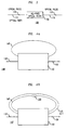
- the all-pass optical filter of the present invention has a structure which includes at least one feedback path, a splitter/combiner, an input port, and an output port.
- the splitter/combiner is coupled to at least one of the feedback paths, the input port, and the output port.
- the splitter/combiner determines what portion of an input optical pulse is provided to the at least one feedback paths. Thereafter, the at least one feedback path applies the desired phase response to the optical pulses transmitted through the all-pass optical filter.
- Each of the at least one feedback paths forms a loop having a path length.
- the path lengths of each feedback path are optionally different. Feedback paths with different path lengths are desirable because they potentially increase the free spectral range (FSR) of the all-pass optical filter.
- FSR free spectral range
- the feedback path of the all-pass optical filter has a ring resonator structure.
- the ring resonator structure includes one or more ring resonators where each of the ring resonators is a closed loop.
- the one or more ring resonators are optionally arranged as a ring cascade or as a series of coupled rings.
- the ring cascade couples a first ring resonator with a splitter/combiner and then the remaining ring resonators are coupled one to another.
- each ring is independently coupled to a splitter/combiner.
- the photonic band gap (PGB) structure includes periodic layers of a material which confine a range of frequencies within such periodic layers. Defects formed in a 2-dimensional array of such layers (2-D PBG) provides a guided feedback path for optical pulses propagated therein. Point defects optionally formed at the edges of the 2-D PBG structure perform the functions of the splitter/combiner, coupling optical signals into and away from such feedback path.
- a plurality of all-pass optical filters of the present invention are suited for use in an optical communication system.
- the plurality of all-pass optical filters are optionally arranged as a concatenated series.
- the optical pulse 120 transmitted in optical communication system 100 is input into the all-pass optical filter 130 .
- the all-pass optical filter 130 reduces the dispersion of the optical pulses transmitted therethrough.
- the all-pass optical filter 130 reduces the dispersion of optical pulses by applying a desired phase response to optical pulses transmitted therethrough.
- the desired phase response applies a frequency-dependent time delay to each frequency of each wave in the packet of waves contained in the optical pulse.
- Application of the frequency-dependent time delay to each frequency of each wave in the packet of waves contained in the optical pulse causes the total group delay of pulses transmitted through the all-pass optical filter to approximate a constant value.
- the dispersion of the optical pulse reduces to about zero.
- the all-pass optical filter 130 of the present invention also has a frequency independent amplitude response. That is, the amplitude of each frequency of the optical pulse transmitted through the all-pass optical filter is substantially preserved.
- an optical pulse 120 enters the all-pass optical filter, a portion of the optical pulse is provided to the feedback path 145 .
- the portion of the optical pulse provided to the feedback path 145 circulates repeatedly therein. However, at each pass of the optical pulse in the feedback path 145 , some portion thereof is provided through the splitter/combiner 143 to the output port 150 . Providing some portion of the optical pulse circulating in the feedback path 145 through the splitter/combiner 143 to the output port 145 , incrementally reduces the portion of the optical pulse introduced into the feedback path 145 , in effect removing it therefrom.
- Coupling ratios for the splitter/combiner 143 and the feedback path 145 determine the portions of the optical pulse 120 that are coupled into and away from the feedback path 145 .
- the magnitude of the coupling ratios for the splitter/combiner 143 and the feedback path 145 are a matter of design choice.
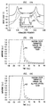
- FIG. 5 is a graph of the group delay of an all-pass optical filter having one feedback path.
- the normalized frequency, ( f 1 - f 0 )/free spectral range (FSR) is plotted as a function of the time delay.
- Frequencies in the packet of frequencies of the optical pulse that fit an integer number of wavelengths on the feedback path are termed resonant frequencies and have a normalized frequency equal to zero, denoted as 170 on the graph of FIG. 5.
- the maximum time delays are applied to the resonant frequencies 170 .
- Frequencies that do not fit an integer number of wavelengths on the feedback path are termed off-resonant frequencies.
- Time delays less than the maximum time delays are applied to the off-resonant frequencies.
- frequencies that are resonant frequencies 170 have a time delay of about 20 au (arbitrary units) applied thereto, while off-resonant frequencies located at a point A on the graph of FIG. 5, denoted as 175 , with a normalized frequency of about -0.05 have a time delay of about 2.5 au applied thereto.
- the optical pulse is output from the all-pass optical filter through the output port 150 .
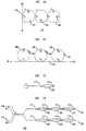
- the at least one feedback path of the all-pass optical filter has a ring resonator structure, as shown in FIGS. 6A-6B.
- the ring resonator structure includes one or more ring resonators 180 wherein each of the ring resonators is a closed loop.
- the one or more ring resonators are optionally arranged as a ring cascade or as a series of coupled rings.
- FIG. 6B shows the ring cascade structure, wherein each ring resonator 180 is independently coupled to a splitter/combiner 178 .
- the feedback path has a length which includes the length of each of the ring resonators 180 .
- the splitter/combiner design sets the values for z k , wherein z k ⁇ 1. From equation (1), the all-pass optical filter has an amplitude response of
- 1. Such an amplitude response for the all-pass optical filter means that all frequencies in the packet of frequencies pass through the filter without a change in their amplitudes.
- the dispersion is proportional to d ⁇ / df , so when the time delay of the output optical pulse, ⁇ o ( f ), approximates a constant value, the dispersion of the optical pulse is expressed as d ⁇ o df ⁇ 0
- the all-pass filter is designed. Filter parameters such as the number of stages (feedback paths), feedback path lengths, and splitter/combiner coupling ratios which best approximate - ⁇ I ( f ) + constant are used to design the all-pass optical filter. An optimization routine may be used to obtain design values which minimize a given error condition.
- FIGS. 9A and 9B Another embodiment of the all-pass optical filter of the present invention forms the feedback path from a Mach-Zehnder Interferometer (MZI) as shown in FIGS. 9A and 9B.
- MZI Mach-Zehnder Interferometer
- FIG. 9A has more than one coupler, denoted as 308 .
- a phase shifter 305 is optionally used to tune the coupling of optical pulses into and out of the feedback path, providing a tunable all-pass optical filter.
- the couplers 308 are optionally identical.
- the MZI structures shown in FIGS. 9A - 9B, are folded to minimize any increase in the feedback path length. In Fig.
- each arm 303, 304 are made substantially identical by crossing the waveguide arms.
- optical signal loss is reduced by increasing the crossing angle for the waveguide arms.
- Crossing the waveguide arms is desirable for large feedback coupling because the effective ⁇ can be made large without affecting fabrication tolerances.
- the all-pass optical filter of the present invention is optionally suitable for delaying the transmission of optical pulses in time.
- the all-pass optical filter delays the transmission of optical signals by lengthening the time delay of optical pulses transmitted therethrough.
- the number of stages for the all-pass optical filter are determined. For this example, assume 4 stages.
- the all-pass optical filter's group delay response depends on its pole locations. Both a magnitude and a phase must be specified for each pole.
- the pole locations are determined from H(z) (see equation 1). An initial choice for the pole locations is made to start the optimization process. The pole locations are then varied to minimize an error criterion.
- the all-pass optical filter has a group delay characteristic, denoted as 408 in FIG. 10A.
- the Gaussian pulse having a pulse characteristic described by 415 is transmitted through the all-pass optical filter with the parameters described above, the dispersion of the resulting optical pulse 425 , is reduced as shown in FIG. 10C.
- All-pass optical filters are also useful for delaying an optical pulse in time.
- a 4 th order all-pass filter is chosen to approximate a delay time of 16 au (arbitrary units) over the normalized frequency range of 0.4 to 0.6.
- the filter parameters for a cascade structure using either rings ( ⁇ , ⁇ ) or cavities ( ⁇ , ⁇ + ⁇ + ⁇ ) are shown in TABLE 2.
- the time delay for an all-pass optical filter with the parameters described above is shown in FIG. 11.
- the group delay applied to frequencies within the passband is essentially constant and much larger than the group delay applied to frequencies outside the passband.
- An all-pass filter described below compensates for the dispersion slope of an optical fiber.
- the all-pass optical filter is designed to compensate the dispersion slope of 250 km of fiber over a 40 nm range.
- the difference in dispersion at 1525 nm and 1565 nm is designed to be 800 ps/nm, with the longest wavelength having the most negative dispersion.
- the FSR is chosen to be an integer multiple of the system channel spacing. For this example a value of 25 GHz is selected.
- the bandwidth over which the dispersion approximates a constant value is about 5 GHz.
- the all-pass optical filter parameters phase, partial reflectors or couplers are optimized at several wavelengths over the 40 nm range for the specific dispersion required at each wavelength.
Landscapes
- Physics & Mathematics (AREA)
- Engineering & Computer Science (AREA)
- Optics & Photonics (AREA)
- Chemical & Material Sciences (AREA)
- General Physics & Mathematics (AREA)
- Signal Processing (AREA)
- Computer Networks & Wireless Communication (AREA)
- Dispersion Chemistry (AREA)
- Nanotechnology (AREA)
- Power Engineering (AREA)
- Microelectronics & Electronic Packaging (AREA)
- Life Sciences & Earth Sciences (AREA)
- Biophysics (AREA)
- Crystallography & Structural Chemistry (AREA)
- Electromagnetism (AREA)
- Optical Communication System (AREA)
- Light Guides In General And Applications Therefor (AREA)
- Optical Integrated Circuits (AREA)
Applications Claiming Priority (2)
| Application Number | Priority Date | Filing Date | Title |
|---|---|---|---|
| US182980 | 1998-10-30 | ||
| US09/182,980 US6289151B1 (en) | 1998-10-30 | 1998-10-30 | All-pass optical filters |
Publications (2)
| Publication Number | Publication Date |
|---|---|
| EP0997751A2 true EP0997751A2 (fr) | 2000-05-03 |
| EP0997751A3 EP0997751A3 (fr) | 2000-12-13 |
Family
ID=22670908
Family Applications (1)
| Application Number | Title | Priority Date | Filing Date |
|---|---|---|---|
| EP99308189A Withdrawn EP0997751A3 (fr) | 1998-10-30 | 1999-10-18 | Filtre optique passe-tout |
Country Status (4)
| Country | Link |
|---|---|
| US (1) | US6289151B1 (fr) |
| EP (1) | EP0997751A3 (fr) |
| JP (1) | JP2000151513A (fr) |
| CA (1) | CA2281486A1 (fr) |
Cited By (13)
| Publication number | Priority date | Publication date | Assignee | Title |
|---|---|---|---|---|
| WO2001090792A1 (fr) * | 2000-05-24 | 2001-11-29 | Bae Systems Electronics Limited | Transformation d'impulsions electriques utilisant des lignes de retard optiques |
| JP2002022983A (ja) * | 2000-05-17 | 2002-01-23 | Lucent Technol Inc | フリースペクトルレンジを大きくした同調型オールパス光学フィルタ |
| US6522450B2 (en) | 2001-04-25 | 2003-02-18 | Corning Incorporated | Loss-less tunable per-channel dispersion compensator |
| US6621614B1 (en) | 2001-08-10 | 2003-09-16 | Arista Networks, Inc. | Etalons with variable reflectivity |
| US6628859B2 (en) | 2001-03-22 | 2003-09-30 | Triquint Technology Holding Co. | Broadband mode converter |
| WO2004001469A1 (fr) * | 2002-06-21 | 2003-12-31 | Teraxion Inc. | Interferometres a reseaux de bragg sur fibres destines a compenser la dispersion chromatique |
| EP1388961A1 (fr) * | 2002-08-06 | 2004-02-11 | Alcatel | Procédé d'asservissement adaptatif permettant une compensation de la dispersion chromatique |
| GB2393264A (en) * | 2002-09-19 | 2004-03-24 | Univ Bristol | Optical photonic crystal waveguide filter |
| WO2004046776A1 (fr) * | 2002-11-18 | 2004-06-03 | National Institute Of Advanced Industrial Science And Technology | Anneau optique comprenant un cristal photonique |
| WO2004063797A1 (fr) * | 2003-01-15 | 2004-07-29 | Bussan Nanotech Research Institute, Inc. | Element de compensation de dispersion, cristal optique, systeme de compensation de dispersion, procede de compensation de dispersion |
| WO2004099848A1 (fr) * | 2003-05-08 | 2004-11-18 | Fujitsu Limited | Compensateur de pente de dispersion |
| US7050671B1 (en) | 2003-01-17 | 2006-05-23 | Jds Uniphase Corporation | Tunable compensation of chromatic dispersion using etalons with tunable optical path length and non-tunable reflectivity |
| US7283997B1 (en) | 2003-05-14 | 2007-10-16 | Apple Inc. | System and method for ranking the relevance of documents retrieved by a query |
Families Citing this family (76)
| Publication number | Priority date | Publication date | Assignee | Title |
|---|---|---|---|---|
| US6996310B2 (en) * | 1997-06-09 | 2006-02-07 | Cambrius, Inc. | Directional-coupler assisted add/drop filter with induced on/off switching and modulation |
| DE69942932D1 (de) * | 1998-06-16 | 2010-12-23 | Xtera Comm Inc | Dispersionskompensierendes und verstärkendes optisches element |
| JP3663310B2 (ja) * | 1999-01-26 | 2005-06-22 | 株式会社日立製作所 | 光ビームスポット変換器及びこれを用いた光伝送モジュール並びに光伝送システム |
| US6580534B2 (en) * | 1999-01-27 | 2003-06-17 | Lucent Technologies Inc. | Optical channel selector |
| US6519065B1 (en) * | 1999-11-05 | 2003-02-11 | Jds Fitel Inc. | Chromatic dispersion compensation device |
| US6553158B1 (en) * | 1999-11-23 | 2003-04-22 | Lnl Technologies, Inc. | Tunable resonator having a movable phase shifter |
| US7016615B1 (en) * | 2000-01-28 | 2006-03-21 | Lucent Technologies Inc. | System comprising a single-stage all-pass optical filter |
| US6907156B1 (en) * | 2000-05-17 | 2005-06-14 | Lucent Technologies Inc. | Reconfigurable multi-channel filters having enhanced channel bandwidth |
| US7173551B2 (en) | 2000-12-21 | 2007-02-06 | Quellan, Inc. | Increasing data throughput in optical fiber transmission systems |
| US7177550B1 (en) * | 2001-01-24 | 2007-02-13 | Ball Aerospace & Technologies Corp. | On-axis laser receiver wavelength demultiplexer with integral immersion lensed detectors |
| US6690846B2 (en) * | 2001-03-01 | 2004-02-10 | Chorum Technologies Lp | Dispersion-compensated optical wavelength router |
| US7149256B2 (en) | 2001-03-29 | 2006-12-12 | Quellan, Inc. | Multilevel pulse position modulation for efficient fiber optic communication |
| US7307569B2 (en) | 2001-03-29 | 2007-12-11 | Quellan, Inc. | Increasing data throughput in optical fiber transmission systems |
| IL158211A0 (en) | 2001-04-04 | 2004-05-12 | Quellan Inc | Method and system for decoding multilevel signals |
| US20020176659A1 (en) * | 2001-05-21 | 2002-11-28 | Jds Uniphase Corporation | Dynamically tunable resonator for use in a chromatic dispersion compensator |
| US6791736B2 (en) | 2001-06-19 | 2004-09-14 | Teralum Llc | Optical device for dispersion compensation |
| DE10147169A1 (de) * | 2001-09-25 | 2003-04-30 | Siemens Ag | Anordnung zur Kompensation von Verzerrungen optischer Signale |
| US20030086638A1 (en) * | 2001-11-02 | 2003-05-08 | Inplane Photonics, Inc. | Optical all-pass filter with gain compensation |
| WO2003071731A1 (fr) | 2002-02-15 | 2003-08-28 | Quellan, Inc. | Technique de recuperation d'horloge d'un signal multi-niveaux |
| EP1345342B1 (fr) * | 2002-03-04 | 2004-02-18 | Alcatel | Emetteur optique, système et procédé pour transmission de signaux à débit élévé |
| US6816101B2 (en) | 2002-03-08 | 2004-11-09 | Quelian, Inc. | High-speed analog-to-digital converter using a unique gray code |
| EP1349311A1 (fr) * | 2002-03-21 | 2003-10-01 | Alcatel | Compresseur temporel de paquets optiques à boucle de délais pour transmissions à haut-débits |
| US6748142B2 (en) * | 2002-04-24 | 2004-06-08 | Lucent Technologies Inc. | Integrated optical dual dispersion compensator for compensating both chromatic and polarization mode dispersion |
| JP2003315752A (ja) * | 2002-04-24 | 2003-11-06 | Fujitsu Ltd | 波長分散補償フィルタ |
| JP2003337236A (ja) * | 2002-05-17 | 2003-11-28 | Nec Corp | 光リング共振器、光導波路デバイスならびに光リング共振器の製造方法 |
| US7801446B2 (en) * | 2002-06-14 | 2010-09-21 | Infinera Corporation | Wavelength division multiplexed optical communication system with rapidly-tunable optical filters |
| AU2002328878A1 (en) * | 2002-07-11 | 2004-02-02 | Agilent Technologies, Inc. | Delaying interferometer |
| US7035361B2 (en) | 2002-07-15 | 2006-04-25 | Quellan, Inc. | Adaptive noise filtering and equalization for optimal high speed multilevel signal decoding |
| JP3952944B2 (ja) * | 2002-08-30 | 2007-08-01 | Kddi株式会社 | リング共振回路 |
| IL152195A0 (en) * | 2002-10-09 | 2003-05-29 | Lambda Crossing Ltd | Tunable laser |
| AU2003287628A1 (en) | 2002-11-12 | 2004-06-03 | Quellan, Inc. | High-speed analog-to-digital conversion with improved robustness to timing uncertainty |
| US20040190906A1 (en) * | 2003-03-26 | 2004-09-30 | Jain Ajay R. | Method and apparatus for simultaneous optical compensation of chromatic and polarization mode dispersion |
| JP2005049856A (ja) * | 2003-07-14 | 2005-02-24 | Nec Corp | 可変分散補償器および可変分散補償方法 |
| US7058258B2 (en) | 2003-07-14 | 2006-06-06 | Nec Corporation | Tunable dispersion compensator and method for tunable dispersion compensation |
| US7162120B2 (en) * | 2003-07-18 | 2007-01-09 | Nec Corporation | Tunable dispersion compensator and method for tunable dispersion compensation |
| US6956991B2 (en) * | 2003-08-05 | 2005-10-18 | Lucent Technologies Inc. | Compact solid-state variable optical delay line with a large continuous tuning range |
| US7212695B2 (en) * | 2003-08-05 | 2007-05-01 | Lucent Technologies Inc. | Variable optical delay line with a large continuous tuning range |
| JP2007502054A (ja) | 2003-08-07 | 2007-02-01 | ケラン インコーポレイテッド | クロストークキャンセルのための方法とシステム |
| US7804760B2 (en) | 2003-08-07 | 2010-09-28 | Quellan, Inc. | Method and system for signal emulation |
| ATE488068T1 (de) | 2003-11-17 | 2010-11-15 | Quellan Inc | Verfahren und system zur löschung von antennenstörungen |
| US7616700B2 (en) | 2003-12-22 | 2009-11-10 | Quellan, Inc. | Method and system for slicing a communication signal |
| JP2005274927A (ja) * | 2004-03-24 | 2005-10-06 | Furukawa Electric Co Ltd:The | フォトニック結晶デバイス |
| JP4284540B2 (ja) * | 2004-11-04 | 2009-06-24 | 独立行政法人産業技術総合研究所 | 光バッファメモリ |
| US7725079B2 (en) | 2004-12-14 | 2010-05-25 | Quellan, Inc. | Method and system for automatic control in an interference cancellation device |
| US7522883B2 (en) | 2004-12-14 | 2009-04-21 | Quellan, Inc. | Method and system for reducing signal interference |
| CA2499651A1 (fr) * | 2005-03-04 | 2006-09-04 | Itf Technologies Optiques Inc./Itf Optical Technologies Inc. | Interferometre a retard commande par phase et dote entierement de fibres, et methode de fabrication de cet appareil |
| EP1896886A1 (fr) * | 2005-06-30 | 2008-03-12 | Pirelli & C. S.p.A. | Procede et systeme pour le traitement optique accordable sans a-coups |
| US8032027B2 (en) | 2005-07-25 | 2011-10-04 | Massachusetts Institute Of Technology | Wide free-spectral-range, widely tunable and hitless-switchable optical channel add-drop filters |
| US7403679B2 (en) * | 2006-03-31 | 2008-07-22 | Intel Corporation | Thermally tunable optical dispersion compensation devices |
| WO2007127369A2 (fr) | 2006-04-26 | 2007-11-08 | Quellan, Inc. | Méthode et système de réduction des émissions rayonnées depuis un canal de communication |
| EP1857846B1 (fr) * | 2006-05-19 | 2017-02-22 | Lumentum Operations LLC | Interféromètre de Mach-Zehnder asymétrique doté d'une tension d'entraînement réduite couplé à un réseau de guide d'ondes compact à faible perte |
| US8105758B2 (en) * | 2006-07-11 | 2012-01-31 | Massachusetts Institute Of Technology | Microphotonic maskless lithography |
| WO2008021467A2 (fr) * | 2006-08-16 | 2008-02-21 | Massachusetts Institute Of Technology | Circulateurs à dérivation équilibrée et interféromètres à équilibre universel repliés |
| WO2008037077A1 (fr) * | 2006-09-26 | 2008-04-03 | Universite Laval | Filtres optiques à cavités multiples à réponses en temps de propagation de groupe parabolique inverse |
| WO2008082664A2 (fr) * | 2006-12-29 | 2008-07-10 | Massachusetts Institute Of Technology | Guides d'ondes et résonateurs tolérants aux erreurs de fabrication |
| US8655114B2 (en) * | 2007-03-26 | 2014-02-18 | Massachusetts Institute Of Technology | Hitless tuning and switching of optical resonator amplitude and phase responses |
| US7539375B2 (en) * | 2007-05-04 | 2009-05-26 | Massachusetts Institute Of Technology | Optical coupled resonator structures based on loop-coupled cavities and loop coupling phase |
| WO2009055440A2 (fr) * | 2007-10-22 | 2009-04-30 | Massachusetts Institute Of Technology | Guidage d'ondes de bloch à faible perte dans des structures ouvertes et réseaux de croisement de guides d'onde efficaces extrêmement compacts |
| US7706045B2 (en) * | 2007-10-26 | 2010-04-27 | Oclaro North America, Inc. | Continuously tunable optical dispersion compensation synthesizers using cascaded etalons |
| US8488922B2 (en) * | 2007-11-02 | 2013-07-16 | Infinera Corporation | Multi-channel dispersion compensator |
| US8073333B2 (en) * | 2007-11-16 | 2011-12-06 | Alcatel Lucent | Multiplex delay unit |
| US7945165B2 (en) * | 2007-11-16 | 2011-05-17 | Alcatel-Lucent Usa Inc. | Optical signal synchronizer |
| US8213799B2 (en) * | 2008-02-22 | 2012-07-03 | Infinera Corporation | Optical receiver including a filter on a planar lightwave circuit |
| US7920770B2 (en) * | 2008-05-01 | 2011-04-05 | Massachusetts Institute Of Technology | Reduction of substrate optical leakage in integrated photonic circuits through localized substrate removal |
| US8406586B2 (en) * | 2008-09-05 | 2013-03-26 | Morton Photonics Inc. | Tunable optical group delay |
| WO2010065710A1 (fr) | 2008-12-03 | 2010-06-10 | Massachusetts Institute Of Technology | Modulateurs optiques résonants |
| US8483521B2 (en) | 2009-05-29 | 2013-07-09 | Massachusetts Institute Of Technology | Cavity dynamics compensation in resonant optical modulators |
| US8260142B2 (en) * | 2009-06-29 | 2012-09-04 | Alcatel Lucent | Multi-channel optical arrayed time buffer |
| US8970945B2 (en) * | 2012-07-24 | 2015-03-03 | University of Zagreb, Faculty of Electrical Engineering and Computing | Modulation averaging reflectors |
| FR3010196B1 (fr) * | 2013-09-02 | 2015-09-18 | Commissariat Energie Atomique | Dispositif de generation d'une modulation d'un signal optique |
| WO2017068430A2 (fr) * | 2015-10-23 | 2017-04-27 | Octrolix Bv | Circuits optiques planaires (plc) présentant une transmissivité et une réflectivité commandables |
| US11320587B2 (en) * | 2015-10-23 | 2022-05-03 | Lionix International Bv | Planar lightwave circuits (PLCs) exhibiting controllable transmissivity / reflectivity |
| US9991966B1 (en) * | 2017-01-06 | 2018-06-05 | Huawei Technologies Canada Co., Ltd. | Optical transmitter |
| US10911845B1 (en) * | 2019-07-11 | 2021-02-02 | Huawei Technologies Co., Ltd. | Apparatus and method for tunable photonic delay |
| FR3107400B1 (fr) * | 2020-02-19 | 2022-02-04 | Commissariat Energie Atomique | Dispositif d’émission laser à effet Vernier accordable |
| CN113179132B (zh) * | 2021-03-26 | 2022-07-29 | 北京邮电大学 | 一种光傅里叶变换芯片及系统 |
Citations (2)
| Publication number | Priority date | Publication date | Assignee | Title |
|---|---|---|---|---|
| EP0984306A1 (fr) * | 1998-09-02 | 2000-03-08 | Lucent Technologies Inc. | Article comprenant une fibre optique à maintien de polarisation avec un réseau de Bragg à période modulée |
| DE19915139A1 (de) * | 1999-03-26 | 2000-09-28 | Deutsche Telekom Ag | Verfahren zur Dispersionskompensation gemeinsam übertragener optischer Signale mit unterschiedlichen Wellenlängen |
Family Cites Families (6)
| Publication number | Priority date | Publication date | Assignee | Title |
|---|---|---|---|---|
| US4768850A (en) | 1984-06-20 | 1988-09-06 | The Board Of Trustees Of The Leland Stanford Junior University | Cascaded fiber optic lattice filter |
| US4934777A (en) * | 1989-03-21 | 1990-06-19 | Pco, Inc. | Cascaded recirculating transmission line without bending loss limitations |
| US5023947A (en) | 1989-11-01 | 1991-06-11 | At&T Bell Laboratories | Optical equalization receiver for lightwave communication systems |
| US5557468A (en) | 1995-05-16 | 1996-09-17 | Jds Fitel Inc | Chromatic dispersion compensation device |
| US5838851A (en) * | 1996-06-24 | 1998-11-17 | Trw Inc. | Optical-loop signal processing using reflection mechanisms |
| US5943457A (en) * | 1998-03-24 | 1999-08-24 | Telecommunications Research Laboratories | Generalized resonant coupler filters |
-
1998
- 1998-10-30 US US09/182,980 patent/US6289151B1/en not_active Expired - Lifetime
-
1999
- 1999-09-09 CA CA002281486A patent/CA2281486A1/fr not_active Abandoned
- 1999-10-18 EP EP99308189A patent/EP0997751A3/fr not_active Withdrawn
- 1999-10-29 JP JP11308937A patent/JP2000151513A/ja active Pending
Patent Citations (2)
| Publication number | Priority date | Publication date | Assignee | Title |
|---|---|---|---|---|
| EP0984306A1 (fr) * | 1998-09-02 | 2000-03-08 | Lucent Technologies Inc. | Article comprenant une fibre optique à maintien de polarisation avec un réseau de Bragg à période modulée |
| DE19915139A1 (de) * | 1999-03-26 | 2000-09-28 | Deutsche Telekom Ag | Verfahren zur Dispersionskompensation gemeinsam übertragener optischer Signale mit unterschiedlichen Wellenlängen |
Cited By (19)
| Publication number | Priority date | Publication date | Assignee | Title |
|---|---|---|---|---|
| JP2002022983A (ja) * | 2000-05-17 | 2002-01-23 | Lucent Technol Inc | フリースペクトルレンジを大きくした同調型オールパス光学フィルタ |
| EP1158326A3 (fr) * | 2000-05-17 | 2004-02-04 | Lucent Technologies Inc. | Filtres optiques passe-tout ajustables ayant de larges intervalles spectraux libres |
| EP2026123A3 (fr) * | 2000-05-17 | 2009-04-01 | Lucent Technologies Inc. | Filtres optiques passe-tout réglables avec des gammes spectrales larges |
| WO2001090792A1 (fr) * | 2000-05-24 | 2001-11-29 | Bae Systems Electronics Limited | Transformation d'impulsions electriques utilisant des lignes de retard optiques |
| US7239809B2 (en) | 2000-05-24 | 2007-07-03 | Bae Systems Plc | Electrical pulse transformation using optical delay lines |
| US6628859B2 (en) | 2001-03-22 | 2003-09-30 | Triquint Technology Holding Co. | Broadband mode converter |
| US6522450B2 (en) | 2001-04-25 | 2003-02-18 | Corning Incorporated | Loss-less tunable per-channel dispersion compensator |
| US6621614B1 (en) | 2001-08-10 | 2003-09-16 | Arista Networks, Inc. | Etalons with variable reflectivity |
| WO2004001469A1 (fr) * | 2002-06-21 | 2003-12-31 | Teraxion Inc. | Interferometres a reseaux de bragg sur fibres destines a compenser la dispersion chromatique |
| US6842547B2 (en) | 2002-08-06 | 2005-01-11 | Alcatel | Adaptive chromatic dispersion compensator |
| EP1388961A1 (fr) * | 2002-08-06 | 2004-02-11 | Alcatel | Procédé d'asservissement adaptatif permettant une compensation de la dispersion chromatique |
| GB2393264A (en) * | 2002-09-19 | 2004-03-24 | Univ Bristol | Optical photonic crystal waveguide filter |
| WO2004046776A1 (fr) * | 2002-11-18 | 2004-06-03 | National Institute Of Advanced Industrial Science And Technology | Anneau optique comprenant un cristal photonique |
| WO2004063797A1 (fr) * | 2003-01-15 | 2004-07-29 | Bussan Nanotech Research Institute, Inc. | Element de compensation de dispersion, cristal optique, systeme de compensation de dispersion, procede de compensation de dispersion |
| US7515785B2 (en) | 2003-01-15 | 2009-04-07 | Fujikura Ltd. | Dispersion compensation element, optical crystal, dispersion compensation system, dispersion compensation method |
| US7050671B1 (en) | 2003-01-17 | 2006-05-23 | Jds Uniphase Corporation | Tunable compensation of chromatic dispersion using etalons with tunable optical path length and non-tunable reflectivity |
| WO2004099848A1 (fr) * | 2003-05-08 | 2004-11-18 | Fujitsu Limited | Compensateur de pente de dispersion |
| US7171076B2 (en) | 2003-05-08 | 2007-01-30 | Fujitsu Limited | Dispersion-slope compensator |
| US7283997B1 (en) | 2003-05-14 | 2007-10-16 | Apple Inc. | System and method for ranking the relevance of documents retrieved by a query |
Also Published As
| Publication number | Publication date |
|---|---|
| US6289151B1 (en) | 2001-09-11 |
| EP0997751A3 (fr) | 2000-12-13 |
| JP2000151513A (ja) | 2000-05-30 |
| CA2281486A1 (fr) | 2000-04-30 |
Similar Documents
| Publication | Publication Date | Title |
|---|---|---|
| US6289151B1 (en) | All-pass optical filters | |
| US6580534B2 (en) | Optical channel selector | |
| Madsen et al. | Optical all-pass filters for phase response design with applications for dispersion compensation | |
| Madsen et al. | Integrated all-pass filters for tunable dispersion and dispersion slope compensation | |
| US6222958B1 (en) | Optical interleaver/de-interleaver | |
| EP1098211A1 (fr) | Dispositif pour compenser la dispersion chromatique | |
| US6907167B2 (en) | Optical interleaving with enhanced spectral response and reduced polarization sensitivity | |
| EP1164724B1 (fr) | Compensateur de dispersion de polarisation de mode pour un système de communication à fibre optique | |
| CA2613105C (fr) | Procede et systeme pour le traitement optique accordable sans a-coups | |
| US6870679B2 (en) | Multi-pass configurations | |
| JP4022766B2 (ja) | 波長分散デバイス | |
| Madsen et al. | An integrated tunable chromatic dispersion compensator for 40 Gb/s NRZ and CSRZ | |
| US7206477B2 (en) | Optical all pass filter device having improved time-bandwidth behavior | |
| Madsen | Subband all-pass filter architectures with applications to dispersion and dispersion-slope compensation and continuously variable delay lines | |
| US6559992B2 (en) | Adjustable chromatic dispersion compensation | |
| US7116907B1 (en) | Acousto-optical tunable filters cascaded together | |
| CN105700082A (zh) | 基于硅基迈克尔逊gt干涉仪的可调交织器 | |
| GB2351625A (en) | Wavelength selective power level control using a plurality of attenuators | |
| US20030086638A1 (en) | Optical all-pass filter with gain compensation | |
| US20030228095A1 (en) | System for and method of replicating optical pulses | |
| Madsen et al. | Integrated optical allpass filters for dispersion compensation | |
| Lenz et al. | Optical filter dispersion in wdm systems: A review | |
| Kaalund et al. | Novel optical wavelength interleaver based on symmetrically parallel-coupled and apodized ring resonator arrays | |
| Takahashi et al. | +/–1350 ps/nm Tuning Demonstration of Tunable Chromatic Dispersion Compensator Based on Silica Waveguide Ring Resonator with Symmetric MZI Coupler | |
| Takahashi et al. | Expansion of passband of tunable chromatic dispersion compensator based on ring resonators using negative group delay peak |
Legal Events
| Date | Code | Title | Description |
|---|---|---|---|
| PUAI | Public reference made under article 153(3) epc to a published international application that has entered the european phase |
Free format text: ORIGINAL CODE: 0009012 |
|
| 17P | Request for examination filed |
Effective date: 19991027 |
|
| AK | Designated contracting states |
Kind code of ref document: A2 Designated state(s): AT BE CH CY DE DK ES FI FR GB GR IE IT LI LU MC NL PT SE |
|
| AX | Request for extension of the european patent |
Free format text: AL;LT;LV;MK;RO;SI |
|
| PUAL | Search report despatched |
Free format text: ORIGINAL CODE: 0009013 |
|
| AK | Designated contracting states |
Kind code of ref document: A3 Designated state(s): AT BE CH CY DE DK ES FI FR GB GR IE IT LI LU MC NL PT SE |
|
| AX | Request for extension of the european patent |
Free format text: AL;LT;LV;MK;RO;SI |
|
| 17Q | First examination report despatched |
Effective date: 20010207 |
|
| AKX | Designation fees paid | ||
| REG | Reference to a national code |
Ref country code: DE Ref legal event code: 8566 |
|
| STAA | Information on the status of an ep patent application or granted ep patent |
Free format text: STATUS: THE APPLICATION IS DEEMED TO BE WITHDRAWN |
|
| 18D | Application deemed to be withdrawn |
Effective date: 20010818 |