EP0997809A2 - Direkter digitaler Synthetisierer - Google Patents
Direkter digitaler Synthetisierer Download PDFInfo
- Publication number
- EP0997809A2 EP0997809A2 EP99308204A EP99308204A EP0997809A2 EP 0997809 A2 EP0997809 A2 EP 0997809A2 EP 99308204 A EP99308204 A EP 99308204A EP 99308204 A EP99308204 A EP 99308204A EP 0997809 A2 EP0997809 A2 EP 0997809A2
- Authority
- EP
- European Patent Office
- Prior art keywords
- digital
- signal
- digital synthesizer
- counter
- synthesizer
- Prior art date
- Legal status (The legal status is an assumption and is not a legal conclusion. Google has not performed a legal analysis and makes no representation as to the accuracy of the status listed.)
- Withdrawn
Links
Images


Classifications
-
- H—ELECTRICITY
- H03—ELECTRONIC CIRCUITRY
- H03L—AUTOMATIC CONTROL, STARTING, SYNCHRONISATION OR STABILISATION OF GENERATORS OF ELECTRONIC OSCILLATIONS OR PULSES
- H03L7/00—Automatic control of frequency or phase; Synchronisation
- H03L7/06—Automatic control of frequency or phase; Synchronisation using a reference signal applied to a frequency- or phase-locked loop
- H03L7/16—Indirect frequency synthesis, i.e. generating a desired one of a number of predetermined frequencies using a frequency- or phase-locked loop
- H03L7/22—Indirect frequency synthesis, i.e. generating a desired one of a number of predetermined frequencies using a frequency- or phase-locked loop using more than one loop
- H03L7/23—Indirect frequency synthesis, i.e. generating a desired one of a number of predetermined frequencies using a frequency- or phase-locked loop using more than one loop with pulse counters or frequency dividers
-
- G—PHYSICS
- G06—COMPUTING OR CALCULATING; COUNTING
- G06F—ELECTRIC DIGITAL DATA PROCESSING
- G06F1/00—Details not covered by groups G06F3/00 - G06F13/00 and G06F21/00
- G06F1/02—Digital function generators
- G06F1/03—Digital function generators working, at least partly, by table look-up
- G06F1/0321—Waveform generators, i.e. devices for generating periodical functions of time, e.g. direct digital synthesizers
Definitions
- the accumulator is essentially an adder circuit with one input and one output. At every clock signal, the input value is added to the current output value and the output of the accumulator assumes a new sum.
- the input usually referred to as a control word, specifies the magnitude of the count increment. If the control word is 250, the accumulator will count in a 0, 250, 500, 750, 1000... sequence until it rolls over and continues.
- An improved direct digital synthesizer simplifies digital circuitry required by utilizing an adder which counts by a predetermined fixed increment (count by C counter).
- a counter is preferably designed using a non-volatile reconfigurable complex programmable logic device (CPLD) IC.
- CPLD complex programmable logic device
- a digital circuit configuration is designed to count only at the required increment loaded into the CPLD.
- Such a specified increment counter provides for a DDS which operates at a much higher frequency than comparable DDS utilizing a general purpose accumulator.
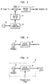
- the present invention is directed to a digital synthesizer 18 of Fig. 2, and preferably a direct digital synthesizer which can operate at a very high frequency.
- the digital synthesizer 18 includes a counter 10, which, upon receiving a clock input, counts by a predetermined fixed increment "C" (wherein "C” is an integer); a memory 12, such as a programmable read only memory (PROM), which stores and outputs digital waveform values upon receiving an input from the counter 10; and a digital-to-analog converter 14 which converts the digital waveform values output from the memory 12 into an analog waveform.
- a counter 10 which, upon receiving a clock input, counts by a predetermined fixed increment "C" (wherein "C” is an integer)
- a memory 12 such as a programmable read only memory (PROM), which stores and outputs digital waveform values upon receiving an input from the counter 10
- PROM programmable read only memory
- the counter 10 is a non-volatile reconfigurable complex programmable logic device (CPLD) IC.
- Such a counter 10 operates at a much higher frequency than a general purpose adder.
- a Cypress Inc. WARP 2 VHDL compiler Version 4.2, was used to generate logic equations for the 24-bit counter 10, counting by a fixed increment of 13,981,013 (decimal), used as an exemplary fixed increment. Any fixed increment can be used and the specific fixed increment discussed herein should be considered limitative of the present invention in any way. Further, the counter 10 being a 24-bit counter is also exemplary as any appropriate size counter counting by any fixed increment can be used.
- the design utilizing the count-by-C counter 10 requires fewer input pins than the standard accumulator 4, and can be fit into a smaller/cheaper/and faster CPLD, having a maximum clock speed of 143.0 Mhz.
- the "+” is the OR operator.
- a list of product terms OR'ed together are in the "sum of products” form.
- the equation states that the Bit[x] will toggle if all the bits specified in the first line are set to “1”, OR if the bits specified in the second line are set to “1”, OR if Bit[x-1] is set to "1".
- a precise signal such as a signal 49.97 MHz for example, is generated utilizing clock 16, digital synthesizer 18, and low-pass filter 20, and is input to mixer 22.
- the input RF signal is mixed with this signal to produce a signal spectrum which contains sum and difference frequencies, as well as other frequency byproducts. For example, if a 30 KHz bandwidth signal is present on a 50 MHz carrier of the RF signal input, and this signal is mixed with the precise 49.97 MHz signal necessary to extract the predetermined or desired signal (50 MHz - 30 KHz), and then filtered, the original or desired 30 KHz signal will be recovered from the output of low-pass filter 24.
- the desired 30 KHz signal is embodied in a carrier wave of the input RF signal.
- the count-by-C type digital synthesizer 18 of the present application is utilized to generate a programmable low frequency clock with precise control.
- a high frequency clock source is input from an external source, such as oscillator component 26.
- the count-by-C digital synthesizer 18 then receives this clock signal and generates an output signal connected to the most significant bit of the counter 10 output.
- the digital synthesizer 18 of the present application is used as a component of a frequency shift keying (FSK) modulator 32. This is shown in Fig. 5.
- FSK frequency shift keying
- the FSK modulator 32 includes a clock 30 for generating a clock frequency signal and a digital synthesizer 18, receiving the clock frequency signal to clock the count-by-C counter 10 thereof.
- the digital synthesizer 18 further receives an input frequency select signal as shown in Fig. 5.
- the frequency select signal is one of two distinct signals (or one of a plurality of distinct signals), such as a relatively high frequency or relatively low frequency signal, each of which triggers the count-by-C counter 10 to count by one of two predetermined fixed increments, C1 or C2 (or one of a plurality of predetermined fixed distinct increments).
- This causes digital synthesizer 18 to generate an output signal of one of two (or a plurality of) distinct frequencies, thereby providing an output of FSK modulator 32.
- the use of the count-by-C type digital synthesizer 18 provides an output of FSK modulator 32 which smoothly transitions between the signals of two (or a plurality of) frequencies. In other words, using the digital synthesizer 18, the FSK modulator 32 easily transitions between signals of two or more frequencies without phase discontinuities.
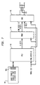
- the digital synthesizer 18 of the present application is used with a single 8-bit memory, such as programmable read only memory (PROM) 44 and a 10-bit DAC 46.
- a microprocessor 40 with a parallel port 40A is connected to a programmable logic device (PLD) 42, used as a count-by-C counter 10.
- PLD programmable logic device
- the PLD 42 connects to both the PROM 44 and to the DAC 46, with the DAC 46 receiving 8 bits of input from PROM 44 and 2 bits of input from PLD 42.
- a common clock such as a 70 MHz clock, is used for each of the PLD 42 as a count-by-C counter 10, PROM 44, and DAC 46. Operation of the digital synthesizer utilizing the PLD 42, PROM 44, and the DAC 46 as shown in Fig. 7 will be explained as follows.
- a memory such as PROM 44 will store all of the components of a waveform to be generated, so that a digital representation of a sinewave (for example) can be output from the memory.
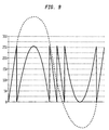
- PROM 44 is essentially an off-the-shelf PROM and as such, is an 8-bit device. Accordingly, the PROM 44 only stores the eight least significant bits (LSBs) of a waveform such as a sinewave. An analog representation of these eight LSBs of the sinewave are shown in Fig. 8 for example.
- DAC 46 is a 10-bit device, since in many applications a 10-bit DAC is required for proper resolution. Thus, typically two 8-bit PROMs would be required to provide the 10 bits used by the 10-bit DAC 46, since a single PROM 44 stores only 8 bits. change at those
- the PLD 42 calculates which angle range it is outputting by evaluating the address output to the PROM 44 and sets bits sine_out [9:8] accordingly.
- the PROM 44 stores a pattern, as shown in Fig. 8 for example, wherein the MSBs are factored out.
- the VHDL code stored in PLD 42, is modified to create Sine__out [9] and Sine__out [8] as follows:
- this VHDL code is translated by the WARP2 VHDL compiler (for example) to a CPLD configuration file which is loaded into the PLD 42 (as an exemplary way to download equations for the count-by-C counter 10).
- the technique is not limited to use with a 10-bit DAC 46, but could also be utilized to generate three or four address bits for use with an 11 or 12-bit DAC, for example.
- the clock is a 70 Mhz clock
- the PROM 44 is a 20 ns PROM
- the DAC 46 is a 100 Mhz DAC
- the PLD 42 is a complex PLD (CPLD), receiving its programming from a microprocessor 40 of a personal computer (not shown).
- CPLD complex PLD
Landscapes
- Engineering & Computer Science (AREA)
- Theoretical Computer Science (AREA)
- Physics & Mathematics (AREA)
- General Engineering & Computer Science (AREA)
- General Physics & Mathematics (AREA)
- Digital Transmission Methods That Use Modulated Carrier Waves (AREA)
- Stabilization Of Oscillater, Synchronisation, Frequency Synthesizers (AREA)
Applications Claiming Priority (2)
| Application Number | Priority Date | Filing Date | Title |
|---|---|---|---|
| US181815 | 1998-10-29 | ||
| US09/181,815 US6539411B1 (en) | 1998-10-29 | 1998-10-29 | Direct digital synthesizer |
Publications (2)
| Publication Number | Publication Date |
|---|---|
| EP0997809A2 true EP0997809A2 (de) | 2000-05-03 |
| EP0997809A3 EP0997809A3 (de) | 2004-02-25 |
Family
ID=22665927
Family Applications (1)
| Application Number | Title | Priority Date | Filing Date |
|---|---|---|---|
| EP99308204A Withdrawn EP0997809A3 (de) | 1998-10-29 | 1999-10-18 | Direkter digitaler Synthetisierer |
Country Status (8)
| Country | Link |
|---|---|
| US (1) | US6539411B1 (de) |
| EP (1) | EP0997809A3 (de) |
| JP (1) | JP3413137B2 (de) |
| KR (1) | KR20000035114A (de) |
| CN (1) | CN1253332A (de) |
| BR (1) | BR9904737A (de) |
| CA (1) | CA2281407A1 (de) |
| TW (1) | TW507424B (de) |
Families Citing this family (10)
| Publication number | Priority date | Publication date | Assignee | Title |
|---|---|---|---|---|
| JP4652546B2 (ja) * | 2000-09-21 | 2011-03-16 | 三星電子株式会社 | 受信機 |
| US7356186B2 (en) * | 2002-08-23 | 2008-04-08 | Kulas Charles J | Digital representation of audio waveforms using peak shifting to provide increased dynamic range |
| US6867625B1 (en) | 2003-09-24 | 2005-03-15 | Itt Manufacturing Enterprises, Inc. | Method and apparatus for high frequency digital carrier synthesis from plural intermediate carrier waveforms |
| US8098376B2 (en) * | 2006-09-07 | 2012-01-17 | William Marsh Rice University | Integrated embedded processor based laser spectroscopic sensor |
| DE102008039205A1 (de) * | 2008-08-22 | 2010-04-22 | EPROTECH Reimann e.K. Jürgen Reimann | Vorrichtung und Verfahren zur Überwachung einzelner Photovoltaikmodule einer Photovoltaikanlage |
| CN103346808B (zh) * | 2013-06-19 | 2015-09-09 | 华为技术有限公司 | 一种终端设备 |
| CN104378082B (zh) | 2013-08-12 | 2017-11-07 | 瑞昱半导体股份有限公司 | 振荡频率偏移侦测方法以及振荡频率偏移侦测电路 |
| TWI551036B (zh) * | 2013-08-22 | 2016-09-21 | 瑞昱半導體股份有限公司 | 振盪頻率偏移偵測方法以及振盪頻率偏移偵測電路 |
| US20150097839A1 (en) * | 2013-10-07 | 2015-04-09 | Tektronix, Inc. | Stochastic rasterization of waveform trace displays |
| CN105933003B (zh) * | 2016-04-25 | 2018-07-17 | 中国科学院武汉物理与数学研究所 | 一种小型铷原子频标射频电路 |
Family Cites Families (12)
| Publication number | Priority date | Publication date | Assignee | Title |
|---|---|---|---|---|
| JPS5818803B2 (ja) | 1975-03-13 | 1983-04-14 | 日本電気株式会社 | デジタル正弦波発生回路 |
| JPS585874A (ja) | 1981-07-01 | 1983-01-13 | Mitsubishi Electric Corp | 波形発生装置 |
| FR2604270B1 (fr) * | 1986-09-22 | 1991-10-18 | Jutand Francis | Additionneur binaire comportant un operande fixe, et multiplieur binaire parallele-serie comprenant un tel additionneur |
| JPH087642B2 (ja) | 1988-02-16 | 1996-01-29 | アンリツ株式会社 | ディジタルファンクションジェネレータ |
| US5028887A (en) | 1989-08-31 | 1991-07-02 | Qualcomm, Inc. | Direct digital synthesizer driven phase lock loop frequency synthesizer with hard limiter |
| US5019825A (en) | 1989-11-24 | 1991-05-28 | The United States Of America As Represented By The Secretary Of The Army | Coherently interruptible frequency hopped chirp generator |
| JPH06504888A (ja) * | 1990-06-05 | 1994-06-02 | コーヒーレント・アイピイ・ライツ・リミテッド | 電力線を介してデータを伝送する方法と装置 |
| JPH0763124B2 (ja) * | 1993-02-24 | 1995-07-05 | 日本電気株式会社 | 直接デジタル周波数シンセサイザ |
| FR2702896B1 (fr) | 1993-03-17 | 1995-06-09 | Sgs Thomson Microelectronics | Generateur multifrequence programmable. |
| JPH09205327A (ja) | 1996-01-29 | 1997-08-05 | Kokusai Electric Co Ltd | 位相制御機能付き直接ディジタル周波数合成回路 |
| US6066967A (en) * | 1997-02-07 | 2000-05-23 | Sensytech, Inc. | Phase-coherent frequency synthesis with a DDS circuit |
| US5963607A (en) * | 1997-05-02 | 1999-10-05 | Ail Systems, Inc. | Direct digital synthesizer with high resolution tracker |
-
1998
- 1998-10-29 US US09/181,815 patent/US6539411B1/en not_active Expired - Lifetime
-
1999
- 1999-08-19 TW TW088114154A patent/TW507424B/zh active
- 1999-09-07 CA CA002281407A patent/CA2281407A1/en not_active Abandoned
- 1999-10-18 EP EP99308204A patent/EP0997809A3/de not_active Withdrawn
- 1999-10-19 BR BR9904737-3A patent/BR9904737A/pt not_active Application Discontinuation
- 1999-10-27 CN CN99123176A patent/CN1253332A/zh active Pending
- 1999-10-29 JP JP30791799A patent/JP3413137B2/ja not_active Expired - Fee Related
- 1999-10-29 KR KR1019990047534A patent/KR20000035114A/ko not_active Withdrawn
Also Published As
| Publication number | Publication date |
|---|---|
| TW507424B (en) | 2002-10-21 |
| KR20000035114A (ko) | 2000-06-26 |
| US6539411B1 (en) | 2003-03-25 |
| CA2281407A1 (en) | 2000-04-29 |
| EP0997809A3 (de) | 2004-02-25 |
| CN1253332A (zh) | 2000-05-17 |
| JP2000151284A (ja) | 2000-05-30 |
| JP3413137B2 (ja) | 2003-06-03 |
| BR9904737A (pt) | 2000-09-05 |
Similar Documents
| Publication | Publication Date | Title |
|---|---|---|
| CN100388156C (zh) | 用于基于快速跳频扩展频谱技术的蜂窝无线通信系统的直接数字频率合成器 | |
| EP1873612A1 (de) | Phasenkohärenter Signalgenerator | |
| US4410955A (en) | Method and apparatus for digital shaping of a digital data stream | |
| EP0443242A2 (de) | Hochauflösender direkter digitaler Synthetisierer | |
| EP0388313A2 (de) | Kohärenter direkter digitaler Synthesizer | |
| EP0997809A2 (de) | Direkter digitaler Synthetisierer | |
| WO2004095458A2 (en) | Method and apparatus for noise shaping in direct digital synthesis circuits | |
| US6281823B1 (en) | Direct digital synthesis using a sine weighted DAC | |
| JP2005198296A (ja) | 多段数値カウンタ発振器 | |
| US4746880A (en) | Number controlled modulated oscillator | |
| US7205800B2 (en) | Clock frequency divider circuit | |
| US5329260A (en) | Numerically-controlled modulated oscillator and modulation method | |
| JP2836526B2 (ja) | 周波数シンセサイザ | |
| US5424664A (en) | Direct digital synthesizer with adjustable clock frequency | |
| EP0782062B1 (de) | Rauschverminderung in digitalen Frequenzsynthetisierern | |
| EP1645027B1 (de) | Verfahren und vorrichtung zur erzeugung beliebiger monozyklus-signalformen | |
| AU2003296435A1 (en) | Wideband dds synthesizer | |
| KR0149126B1 (ko) | 혼합형 주파수 합성기 | |
| US6922089B2 (en) | Digital frequency synthesizing circuit and system thereof using interpolation and linear feedback shift register (LFSR) | |
| MXPA99009836A (en) | Digital synthesizer dire | |
| AU2005312073B2 (en) | Phase persistent agile signal source method, apparatus, and computer program product | |
| Palomäki et al. | Memory Optimized, High Signal Quality Direct Digital Frequency Synthesizer on an FPGA | |
| US7395289B2 (en) | Frequency synthesizing and back-end processing circuit and method thereof | |
| KR100334125B1 (ko) | 개선된 주파수 스펙트럼 특성을 갖는 디지털 주파수 합성기 | |
| KR0175272B1 (ko) | 수치제어 발진기 |
Legal Events
| Date | Code | Title | Description |
|---|---|---|---|
| PUAI | Public reference made under article 153(3) epc to a published international application that has entered the european phase |
Free format text: ORIGINAL CODE: 0009012 |
|
| AK | Designated contracting states |
Kind code of ref document: A2 Designated state(s): AT BE CH CY DE DK ES FI FR GB GR IE IT LI LU MC NL PT SE |
|
| AX | Request for extension of the european patent |
Free format text: AL;LT;LV;MK;RO;SI |
|
| PUAL | Search report despatched |
Free format text: ORIGINAL CODE: 0009013 |
|
| AK | Designated contracting states |
Kind code of ref document: A3 Designated state(s): AT BE CH CY DE DK ES FI FR GB GR IE IT LI LU MC NL PT SE |
|
| AX | Request for extension of the european patent |
Extension state: AL LT LV MK RO SI |
|
| STAA | Information on the status of an ep patent application or granted ep patent |
Free format text: STATUS: THE APPLICATION IS DEEMED TO BE WITHDRAWN |
|
| 18D | Application deemed to be withdrawn |
Effective date: 20040503 |
|
| REG | Reference to a national code |
Ref country code: DE Ref legal event code: 8566 |