EP0999613A1 - Leiterplattensteckverbinder bestehend aus Stecker und Gegenstück - Google Patents
Leiterplattensteckverbinder bestehend aus Stecker und Gegenstück Download PDFInfo
- Publication number
- EP0999613A1 EP0999613A1 EP99402711A EP99402711A EP0999613A1 EP 0999613 A1 EP0999613 A1 EP 0999613A1 EP 99402711 A EP99402711 A EP 99402711A EP 99402711 A EP99402711 A EP 99402711A EP 0999613 A1 EP0999613 A1 EP 0999613A1
- Authority
- EP
- European Patent Office
- Prior art keywords
- plug
- base
- contacts
- edge
- card
- Prior art date
- Legal status (The legal status is an assumption and is not a legal conclusion. Google has not performed a legal analysis and makes no representation as to the accuracy of the status listed.)
- Granted
Links
- 238000003780 insertion Methods 0.000 claims abstract description 14
- 230000037431 insertion Effects 0.000 claims abstract description 14
- 238000005452 bending Methods 0.000 claims description 4
- 238000003032 molecular docking Methods 0.000 claims description 3
- 230000000295 complement effect Effects 0.000 claims description 2
- 230000000630 rising effect Effects 0.000 claims description 2
- 239000004020 conductor Substances 0.000 abstract 1
- 230000015556 catabolic process Effects 0.000 description 2
- 238000004140 cleaning Methods 0.000 description 2
- 238000006731 degradation reaction Methods 0.000 description 2
- 230000000694 effects Effects 0.000 description 2
- 241000446313 Lamella Species 0.000 description 1
- 239000003082 abrasive agent Substances 0.000 description 1
- 230000001174 ascending effect Effects 0.000 description 1
- 230000009286 beneficial effect Effects 0.000 description 1
- 230000006378 damage Effects 0.000 description 1
- 238000012986 modification Methods 0.000 description 1
- 230000004048 modification Effects 0.000 description 1
Images

Classifications
-
- H—ELECTRICITY
- H01—ELECTRIC ELEMENTS
- H01R—ELECTRICALLY-CONDUCTIVE CONNECTIONS; STRUCTURAL ASSOCIATIONS OF A PLURALITY OF MUTUALLY-INSULATED ELECTRICAL CONNECTING ELEMENTS; COUPLING DEVICES; CURRENT COLLECTORS
- H01R12/00—Structural associations of a plurality of mutually-insulated electrical connecting elements, specially adapted for printed circuits, e.g. printed circuit boards [PCB], flat or ribbon cables, or like generally planar structures, e.g. terminal strips, terminal blocks; Coupling devices specially adapted for printed circuits, flat or ribbon cables, or like generally planar structures; Terminals specially adapted for contact with, or insertion into, printed circuits, flat or ribbon cables, or like generally planar structures
- H01R12/70—Coupling devices
- H01R12/71—Coupling devices for rigid printing circuits or like structures
- H01R12/72—Coupling devices for rigid printing circuits or like structures coupling with the edge of the rigid printed circuits or like structures
- H01R12/721—Coupling devices for rigid printing circuits or like structures coupling with the edge of the rigid printed circuits or like structures cooperating directly with the edge of the rigid printed circuits
-
- H—ELECTRICITY
- H01—ELECTRIC ELEMENTS
- H01R—ELECTRICALLY-CONDUCTIVE CONNECTIONS; STRUCTURAL ASSOCIATIONS OF A PLURALITY OF MUTUALLY-INSULATED ELECTRICAL CONNECTING ELEMENTS; COUPLING DEVICES; CURRENT COLLECTORS
- H01R13/00—Details of coupling devices of the kinds covered by groups H01R12/70 or H01R24/00 - H01R33/00
- H01R13/02—Contact members
- H01R13/26—Pin or blade contacts for sliding co-operation on one side only
-
- H—ELECTRICITY
- H01—ELECTRIC ELEMENTS
- H01R—ELECTRICALLY-CONDUCTIVE CONNECTIONS; STRUCTURAL ASSOCIATIONS OF A PLURALITY OF MUTUALLY-INSULATED ELECTRICAL CONNECTING ELEMENTS; COUPLING DEVICES; CURRENT COLLECTORS
- H01R2201/00—Connectors or connections adapted for particular applications
- H01R2201/16—Connectors or connections adapted for particular applications for telephony
Definitions
- the present invention relates to a socket connection intended to come and engage on the edge of a printed circuit board with contacts intended to take elastic support on the part and on the other side of the card to establish a direct connection with conductive connection pads of this menu.
- the invention relates in particular to a socket connection of an accessory to be connected directly to the circuit board of a mobile phone, this phone mobile not having on its connector base input / output but a printed circuit (usually soldered to the input / output connector) directly accessible for connection to an external accessory or sheet.
- the major technical problem posed with this type application relates to the degradation, or even the destruction of contacts by sharp edges abrasives of the printed circuit at the time of insertion, which has the effect of considerably limiting the number of connection / disconnection operations.
- a second problem is to ensure a pressure of sufficient contact between the accessory contacts and the connection areas of the printed circuit.
- the object of the invention is precisely to solve the two problems above.
- the plug contacts do not rub on the outer edges of the map, when the engagement of the plug in the socket.
- the friction on the connection pads is very limited.
- the contacts are supported elastically on the connection areas of the card only when the plug is almost completely engaged on the edge of the card, without degradation of contacts when inserting the plug into the socket.
- the base and the plug comprise means complementary to lock them together at the end of stroke for inserting the plug into the socket.
- the means for move the plug up include ramps rising inside the base and making protruding above a plane passing through the edge bottom of the plug insertion opening, these ramps cooperating with the end of the plug for the move up.
- the means for making bend down the flexible part of the plug include at least one descending ramp located inside the base and protruding below of a plane passing through the upper edge of the opening inserting the plug, this ramp cooperating with the end of said flexible part to make it flex down.
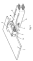
- connection socket intended to come to engage on the edge 2 of a printed circuit board 1, has contacts 3, 4 intended to bear elastically on either side of card 1 to establish a direct connection with conductive pads of connection 5 of this card.
- the socket comprises a base 6 without contacts intended to be fixed on the printed circuit board 1 by lugs hook 19 (fittings).
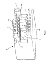
- This base 6 includes a opening 7 to receive a card 8 comprising two parallel rows of elastic contacts 3, 4 intended to be supported on the conductive pads 5, after insertion of plug 8 into opening 7 of base 6.
- one 3 rows of contacts is carried by a first flexible part 9 of the plug 8 which can engage in the opening 7 of the base 6.
- the other row of contacts 4 is carried by a second part 10 of sheet 8 separated from the first part 9 by a recess 11 and can engage under edge 2 of the circuit board printed 1.
- the base 6 and the plug 8 include additional resources for lock together at the end of the insertion stroke of plug 8 in socket 6.
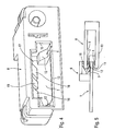
- the means to move plug 8 upwards when insertion into base 6 include two ramps risers 12 located inside the base 6 and protruding above a plane passing through the edge lower 13 of the opening 7 for inserting the plug 8 in the base 6. These ramps 12 cooperate with the end 14a of two guide beams 14 arranged on either side of the flexible part 9 of the sheet 8 to move it up.
- Figure 4 also shows that the ramps 12 are located at a certain distance d from the edge lower 13 of the opening 7 for inserting the plug 8 in base 6.
- the two ramps 12 are each located near a side edge 15 of the opening 7 for introducing sheet 8.
- Means for bending down the flexible part 9 of the plug 8 during its insertion in the base 6 include two descending ramps 16 (see Figure 4) located inside the base 6 and protruding below a plane passing through the edge upper 17 of the opening 7 for inserting the plug 8. These ramps 16 cooperate with the end 9a of the flexible part 9 of the plug to bend it towards the bottom.
- Additional means to lock together the base 6 and the plug 8 include a spout latching 18 (see Figures 2 and 3) formed on the upper face and near the end 9a of the part flexible 9 of the plug 8 cooperating with a lamella flexible 19 (see FIG. 4) formed in the base 6.
- connection socket that we have just described works as follows:
- the lower row 4 of contacts rests elastically on the ranges of connection 5 provided on the underside of the card.
- the spout 18 located at the front of the flexible part 9 of the plug 8 snaps onto the end of the strip 19 located inside the base 6, thus locking the plug 8 of the base 6.
Landscapes
- Coupling Device And Connection With Printed Circuit (AREA)
- Details Of Connecting Devices For Male And Female Coupling (AREA)
- Shaping Of Tube Ends By Bending Or Straightening (AREA)
- Addition Polymer Or Copolymer, Post-Treatments, Or Chemical Modifications (AREA)
Applications Claiming Priority (2)
| Application Number | Priority Date | Filing Date | Title |
|---|---|---|---|
| FR9814028 | 1998-11-06 | ||
| FR9814028A FR2785723B1 (fr) | 1998-11-06 | 1998-11-06 | Prise de connexion sur circuit imprime, comprenant une fiche et une embase |
Publications (2)
| Publication Number | Publication Date |
|---|---|
| EP0999613A1 true EP0999613A1 (de) | 2000-05-10 |
| EP0999613B1 EP0999613B1 (de) | 2003-03-05 |
Family
ID=9532486
Family Applications (1)
| Application Number | Title | Priority Date | Filing Date |
|---|---|---|---|
| EP99402711A Expired - Lifetime EP0999613B1 (de) | 1998-11-06 | 1999-10-29 | Leiterplattensteckverbinder bestehend aus Stecker und Gegenstück |
Country Status (9)
| Country | Link |
|---|---|
| US (1) | US6234822B1 (de) |
| EP (1) | EP0999613B1 (de) |
| JP (1) | JP2000188144A (de) |
| CN (1) | CN1253397A (de) |
| AT (1) | ATE233963T1 (de) |
| CA (1) | CA2288414A1 (de) |
| DE (1) | DE69905681T2 (de) |
| FR (1) | FR2785723B1 (de) |
| SG (1) | SG75992A1 (de) |
Families Citing this family (9)
| Publication number | Priority date | Publication date | Assignee | Title |
|---|---|---|---|---|
| US6346012B1 (en) * | 1998-08-15 | 2002-02-12 | Delta Electronics, Inc. | Locking cartridge for conveniently locking very thin connector with near-zero inductance onto PC board |
| JP2002184539A (ja) | 2000-12-14 | 2002-06-28 | Auto Network Gijutsu Kenkyusho:Kk | コネクタ |
| JP4841756B2 (ja) * | 2001-06-08 | 2011-12-21 | 日本圧着端子製造株式会社 | コンタクトとこれを装着した電気コネクタ |
| CN100350312C (zh) * | 2004-11-18 | 2007-11-21 | 友达光电股份有限公司 | 平面显示器以及其背光模块 |
| JP2006302651A (ja) * | 2005-04-20 | 2006-11-02 | Sumitomo Electric Ind Ltd | コネクタ |
| US8496486B2 (en) * | 2010-07-19 | 2013-07-30 | Tyco Electronics Corporation | Transceiver assembly |
| DE102011005479A1 (de) * | 2011-03-14 | 2012-09-20 | Robert Bosch Gmbh | Direktsteckelement mit zwei Federbereichen |
| US9917387B2 (en) * | 2015-06-10 | 2018-03-13 | Osram Gmbh | Connector for lighting devices, corresponding accessory and method |
| CN112421720A (zh) * | 2020-11-10 | 2021-02-26 | 东莞市爱客德电子科技有限公司 | 一种充电坞及充电坞电路 |
Citations (3)
| Publication number | Priority date | Publication date | Assignee | Title |
|---|---|---|---|---|
| EP0036933A2 (de) * | 1980-03-28 | 1981-10-07 | Bohdan Ulrich | Steckverbinder und Verwendung desselben zur Herstellung einer lösbaren elektrischen Verbindung |
| US4863395A (en) * | 1989-01-17 | 1989-09-05 | Robert Babuka | Zero insertion force connector with component card |
| EP0405333A2 (de) * | 1989-06-27 | 1991-01-02 | Siemens Aktiengesellschaft | Andrucksteckverbinder |
Family Cites Families (1)
| Publication number | Priority date | Publication date | Assignee | Title |
|---|---|---|---|---|
| FR2604804B1 (fr) | 1986-10-02 | 1989-12-29 | Francelco Sa | Systeme a lecture de cartes d'identification a contacts electriques |
-
1998
- 1998-11-06 FR FR9814028A patent/FR2785723B1/fr not_active Expired - Fee Related
-
1999
- 1999-10-29 AT AT99402711T patent/ATE233963T1/de not_active IP Right Cessation
- 1999-10-29 DE DE69905681T patent/DE69905681T2/de not_active Expired - Fee Related
- 1999-10-29 EP EP99402711A patent/EP0999613B1/de not_active Expired - Lifetime
- 1999-11-01 SG SG1999005407A patent/SG75992A1/en unknown
- 1999-11-03 CA CA002288414A patent/CA2288414A1/en not_active Abandoned
- 1999-11-05 CN CN99123438A patent/CN1253397A/zh active Pending
- 1999-11-05 US US09/435,263 patent/US6234822B1/en not_active Expired - Fee Related
- 1999-11-08 JP JP11317451A patent/JP2000188144A/ja active Pending
Patent Citations (3)
| Publication number | Priority date | Publication date | Assignee | Title |
|---|---|---|---|---|
| EP0036933A2 (de) * | 1980-03-28 | 1981-10-07 | Bohdan Ulrich | Steckverbinder und Verwendung desselben zur Herstellung einer lösbaren elektrischen Verbindung |
| US4863395A (en) * | 1989-01-17 | 1989-09-05 | Robert Babuka | Zero insertion force connector with component card |
| EP0405333A2 (de) * | 1989-06-27 | 1991-01-02 | Siemens Aktiengesellschaft | Andrucksteckverbinder |
Also Published As
| Publication number | Publication date |
|---|---|
| ATE233963T1 (de) | 2003-03-15 |
| DE69905681T2 (de) | 2003-11-06 |
| JP2000188144A (ja) | 2000-07-04 |
| FR2785723B1 (fr) | 2003-05-23 |
| DE69905681D1 (de) | 2003-04-10 |
| CA2288414A1 (en) | 2000-05-06 |
| SG75992A1 (en) | 2000-10-24 |
| US6234822B1 (en) | 2001-05-22 |
| EP0999613B1 (de) | 2003-03-05 |
| CN1253397A (zh) | 2000-05-17 |
| FR2785723A1 (fr) | 2000-05-12 |
Similar Documents
| Publication | Publication Date | Title |
|---|---|---|
| EP1154527B1 (de) | Verbindungsvorrichtung zur Verbindung zwischen einem Koaxialkabel und einer Leiterplatte | |
| CN101232136B (zh) | 电连接器 | |
| FR2785724A1 (fr) | Connecteur electrique blinde comportant un element de support pour pattes | |
| FR3017253A1 (fr) | Connecteur electrique | |
| EP0999613B1 (de) | Leiterplattensteckverbinder bestehend aus Stecker und Gegenstück | |
| FR2589637A1 (fr) | Element femelle de contacts electriques | |
| FR2806218A1 (fr) | Connecteur d'entree/sortie du type fiche | |
| FR2898734A1 (fr) | Connecteur formant un composant pour montage en surface | |
| EP3170227B1 (de) | Elektrischer verbinder und elektrisches verbindungssystem | |
| FR2647602A1 (fr) | Contact femelle | |
| EP0024981B1 (de) | Elektrische Verbindungen mit Flachsteckhülse und Zungenkontakt | |
| FR2552946A1 (fr) | Connecteur electrique destine a s'accoupler avec trois languettes et borne pour ce connecteur | |
| US6033256A (en) | Slimline plug-in connector | |
| CN100561802C (zh) | 连接器 | |
| US6254400B1 (en) | Connector structure | |
| FR2517480A1 (fr) | Contact electrique femelle | |
| FR2752647A1 (fr) | Dispositif de borne pour un equipement electrique | |
| FR2783361A1 (fr) | Ensemble conecteur blinde pouvant etre monte de maniere ferme sur une carte circuit | |
| FR2701338A1 (fr) | Dispositif pour le raccordement de deux languettes mâles d'organes de contacts électriques. | |
| EP0674357B1 (de) | Gehäuseteilen von elektrischen Verbindern | |
| KR100246005B1 (ko) | 와이어 커넥터 | |
| FR2563950A1 (fr) | Connecteur electrique a contacts multiples et a verrouillage | |
| EP0913885A1 (de) | Anschlussbuchse | |
| FR2781935A1 (fr) | Prise de connexion sur circuit imprime | |
| FR2656471A1 (fr) | Borne electrique femelle pour hautes temperatures. |
Legal Events
| Date | Code | Title | Description |
|---|---|---|---|
| PUAI | Public reference made under article 153(3) epc to a published international application that has entered the european phase |
Free format text: ORIGINAL CODE: 0009012 |
|
| AK | Designated contracting states |
Kind code of ref document: A1 Designated state(s): AT BE CH CY DE DK ES FI FR GB GR IE IT LI LU MC NL PT SE |
|
| AX | Request for extension of the european patent |
Free format text: AL;LT;LV;MK;RO;SI |
|
| 17P | Request for examination filed |
Effective date: 20001020 |
|
| AKX | Designation fees paid |
Free format text: AT BE CH CY DE DK ES FI FR GB GR IE IT LI LU MC NL PT SE |
|
| 17Q | First examination report despatched |
Effective date: 20010724 |
|
| GRAG | Despatch of communication of intention to grant |
Free format text: ORIGINAL CODE: EPIDOS AGRA |
|
| GRAG | Despatch of communication of intention to grant |
Free format text: ORIGINAL CODE: EPIDOS AGRA |
|
| GRAH | Despatch of communication of intention to grant a patent |
Free format text: ORIGINAL CODE: EPIDOS IGRA |
|
| GRAH | Despatch of communication of intention to grant a patent |
Free format text: ORIGINAL CODE: EPIDOS IGRA |
|
| RAP1 | Party data changed (applicant data changed or rights of an application transferred) |
Owner name: FCI |
|
| GRAA | (expected) grant |
Free format text: ORIGINAL CODE: 0009210 |
|
| AK | Designated contracting states |
Designated state(s): AT BE CH CY DE DK ES FI FR GB GR IE IT LI LU MC NL PT SE |
|
| PG25 | Lapsed in a contracting state [announced via postgrant information from national office to epo] |
Ref country code: NL Free format text: LAPSE BECAUSE OF FAILURE TO SUBMIT A TRANSLATION OF THE DESCRIPTION OR TO PAY THE FEE WITHIN THE PRESCRIBED TIME-LIMIT Effective date: 20030305 Ref country code: IT Free format text: LAPSE BECAUSE OF FAILURE TO SUBMIT A TRANSLATION OF THE DESCRIPTION OR TO PAY THE FEE WITHIN THE PRESCRIBED TIME-LIMIT;WARNING: LAPSES OF ITALIAN PATENTS WITH EFFECTIVE DATE BEFORE 2007 MAY HAVE OCCURRED AT ANY TIME BEFORE 2007. THE CORRECT EFFECTIVE DATE MAY BE DIFFERENT FROM THE ONE RECORDED. Effective date: 20030305 Ref country code: IE Free format text: LAPSE BECAUSE OF FAILURE TO SUBMIT A TRANSLATION OF THE DESCRIPTION OR TO PAY THE FEE WITHIN THE PRESCRIBED TIME-LIMIT Effective date: 20030305 Ref country code: GR Free format text: LAPSE BECAUSE OF FAILURE TO SUBMIT A TRANSLATION OF THE DESCRIPTION OR TO PAY THE FEE WITHIN THE PRESCRIBED TIME-LIMIT Effective date: 20030305 Ref country code: FI Free format text: LAPSE BECAUSE OF FAILURE TO SUBMIT A TRANSLATION OF THE DESCRIPTION OR TO PAY THE FEE WITHIN THE PRESCRIBED TIME-LIMIT Effective date: 20030305 Ref country code: AT Free format text: LAPSE BECAUSE OF FAILURE TO SUBMIT A TRANSLATION OF THE DESCRIPTION OR TO PAY THE FEE WITHIN THE PRESCRIBED TIME-LIMIT Effective date: 20030305 |
|
| REG | Reference to a national code |
Ref country code: GB Ref legal event code: FG4D Free format text: NOT ENGLISH |
|
| REG | Reference to a national code |
Ref country code: CH Ref legal event code: EP |
|
| REG | Reference to a national code |
Ref country code: IE Ref legal event code: FG4D Free format text: FRENCH |
|
| REF | Corresponds to: |
Ref document number: 69905681 Country of ref document: DE Date of ref document: 20030410 Kind code of ref document: P |
|
| PG25 | Lapsed in a contracting state [announced via postgrant information from national office to epo] |
Ref country code: SE Free format text: LAPSE BECAUSE OF FAILURE TO SUBMIT A TRANSLATION OF THE DESCRIPTION OR TO PAY THE FEE WITHIN THE PRESCRIBED TIME-LIMIT Effective date: 20030605 Ref country code: PT Free format text: LAPSE BECAUSE OF FAILURE TO SUBMIT A TRANSLATION OF THE DESCRIPTION OR TO PAY THE FEE WITHIN THE PRESCRIBED TIME-LIMIT Effective date: 20030605 Ref country code: DK Free format text: LAPSE BECAUSE OF FAILURE TO SUBMIT A TRANSLATION OF THE DESCRIPTION OR TO PAY THE FEE WITHIN THE PRESCRIBED TIME-LIMIT Effective date: 20030605 |
|
| GBT | Gb: translation of ep patent filed (gb section 77(6)(a)/1977) | ||
| NLV1 | Nl: lapsed or annulled due to failure to fulfill the requirements of art. 29p and 29m of the patents act | ||
| PG25 | Lapsed in a contracting state [announced via postgrant information from national office to epo] |
Ref country code: ES Free format text: LAPSE BECAUSE OF FAILURE TO SUBMIT A TRANSLATION OF THE DESCRIPTION OR TO PAY THE FEE WITHIN THE PRESCRIBED TIME-LIMIT Effective date: 20030930 |
|
| PG25 | Lapsed in a contracting state [announced via postgrant information from national office to epo] |
Ref country code: LU Free format text: LAPSE BECAUSE OF NON-PAYMENT OF DUE FEES Effective date: 20031029 Ref country code: GB Free format text: LAPSE BECAUSE OF NON-PAYMENT OF DUE FEES Effective date: 20031029 Ref country code: CY Free format text: LAPSE BECAUSE OF FAILURE TO SUBMIT A TRANSLATION OF THE DESCRIPTION OR TO PAY THE FEE WITHIN THE PRESCRIBED TIME-LIMIT Effective date: 20031029 |
|
| REG | Reference to a national code |
Ref country code: IE Ref legal event code: FD4D Ref document number: 0999613E Country of ref document: IE |
|
| PG25 | Lapsed in a contracting state [announced via postgrant information from national office to epo] |
Ref country code: MC Free format text: LAPSE BECAUSE OF NON-PAYMENT OF DUE FEES Effective date: 20031031 Ref country code: LI Free format text: LAPSE BECAUSE OF NON-PAYMENT OF DUE FEES Effective date: 20031031 Ref country code: CH Free format text: LAPSE BECAUSE OF NON-PAYMENT OF DUE FEES Effective date: 20031031 Ref country code: BE Free format text: LAPSE BECAUSE OF NON-PAYMENT OF DUE FEES Effective date: 20031031 |
|
| PLBE | No opposition filed within time limit |
Free format text: ORIGINAL CODE: 0009261 |
|
| STAA | Information on the status of an ep patent application or granted ep patent |
Free format text: STATUS: NO OPPOSITION FILED WITHIN TIME LIMIT |
|
| 26N | No opposition filed |
Effective date: 20031208 |
|
| BERE | Be: lapsed |
Owner name: *FCI Effective date: 20031031 |
|
| PG25 | Lapsed in a contracting state [announced via postgrant information from national office to epo] |
Ref country code: DE Free format text: LAPSE BECAUSE OF NON-PAYMENT OF DUE FEES Effective date: 20040501 |
|
| REG | Reference to a national code |
Ref country code: CH Ref legal event code: PL |
|
| GBPC | Gb: european patent ceased through non-payment of renewal fee |
Effective date: 20031029 |
|
| PG25 | Lapsed in a contracting state [announced via postgrant information from national office to epo] |
Ref country code: FR Free format text: LAPSE BECAUSE OF NON-PAYMENT OF DUE FEES Effective date: 20040630 |
|
| REG | Reference to a national code |
Ref country code: FR Ref legal event code: ST |