EP0999640A2 - Dispositif à ondes acoustiques de surface, substrat correspondant et procédé pour la fabrication du substrat - Google Patents
Dispositif à ondes acoustiques de surface, substrat correspondant et procédé pour la fabrication du substrat Download PDFInfo
- Publication number
- EP0999640A2 EP0999640A2 EP99121666A EP99121666A EP0999640A2 EP 0999640 A2 EP0999640 A2 EP 0999640A2 EP 99121666 A EP99121666 A EP 99121666A EP 99121666 A EP99121666 A EP 99121666A EP 0999640 A2 EP0999640 A2 EP 0999640A2
- Authority
- EP
- European Patent Office
- Prior art keywords
- single crystal
- substrate
- buffer layer
- aluminum nitride
- layer
- Prior art date
- Legal status (The legal status is an assumption and is not a legal conclusion. Google has not performed a legal analysis and makes no representation as to the accuracy of the status listed.)
- Withdrawn
Links
- 239000000758 substrate Substances 0.000 title claims abstract description 111
- 238000010897 surface acoustic wave method Methods 0.000 title claims description 57
- 238000004519 manufacturing process Methods 0.000 title claims description 14
- 239000013078 crystal Substances 0.000 claims abstract description 147
- 229910052594 sapphire Inorganic materials 0.000 claims abstract description 96
- PMHQVHHXPFUNSP-UHFFFAOYSA-M copper(1+);methylsulfanylmethane;bromide Chemical compound Br[Cu].CSC PMHQVHHXPFUNSP-UHFFFAOYSA-M 0.000 claims abstract description 92
- 239000010980 sapphire Substances 0.000 claims abstract description 87
- 229910002601 GaN Inorganic materials 0.000 claims abstract description 46
- JMASRVWKEDWRBT-UHFFFAOYSA-N Gallium nitride Chemical compound [Ga]#N JMASRVWKEDWRBT-UHFFFAOYSA-N 0.000 claims abstract description 29
- RNQKDQAVIXDKAG-UHFFFAOYSA-N aluminum gallium Chemical compound [Al].[Ga] RNQKDQAVIXDKAG-UHFFFAOYSA-N 0.000 claims abstract description 17
- 230000001902 propagating effect Effects 0.000 claims abstract description 8
- 238000000034 method Methods 0.000 claims description 18
- 238000000151 deposition Methods 0.000 claims description 12
- 230000008878 coupling Effects 0.000 claims description 8
- 238000010168 coupling process Methods 0.000 claims description 8
- 238000005859 coupling reaction Methods 0.000 claims description 8
- UFHFLCQGNIYNRP-UHFFFAOYSA-N Hydrogen Chemical compound [H][H] UFHFLCQGNIYNRP-UHFFFAOYSA-N 0.000 claims description 7
- 239000000463 material Substances 0.000 claims description 7
- 238000005121 nitriding Methods 0.000 claims description 7
- 239000001257 hydrogen Substances 0.000 claims description 6
- 229910052739 hydrogen Inorganic materials 0.000 claims description 6
- 230000008021 deposition Effects 0.000 claims description 5
- 238000000137 annealing Methods 0.000 claims description 3
- 238000002488 metal-organic chemical vapour deposition Methods 0.000 claims 2
- 239000010408 film Substances 0.000 description 16
- QGZKDVFQNNGYKY-UHFFFAOYSA-N Ammonia Chemical compound N QGZKDVFQNNGYKY-UHFFFAOYSA-N 0.000 description 12
- 230000015572 biosynthetic process Effects 0.000 description 6
- JLTRXTDYQLMHGR-UHFFFAOYSA-N trimethylaluminium Chemical compound C[Al](C)C JLTRXTDYQLMHGR-UHFFFAOYSA-N 0.000 description 6
- XCZXGTMEAKBVPV-UHFFFAOYSA-N trimethylgallium Chemical compound C[Ga](C)C XCZXGTMEAKBVPV-UHFFFAOYSA-N 0.000 description 4
- 229910021529 ammonia Inorganic materials 0.000 description 3
- 238000005229 chemical vapour deposition Methods 0.000 description 3
- 150000001875 compounds Chemical class 0.000 description 3
- 230000003247 decreasing effect Effects 0.000 description 3
- 238000002474 experimental method Methods 0.000 description 3
- 239000007789 gas Substances 0.000 description 3
- 229910052751 metal Inorganic materials 0.000 description 3
- 239000002184 metal Substances 0.000 description 3
- 229910000069 nitrogen hydride Inorganic materials 0.000 description 3
- IJGRMHOSHXDMSA-UHFFFAOYSA-N Atomic nitrogen Chemical compound N#N IJGRMHOSHXDMSA-UHFFFAOYSA-N 0.000 description 2
- 239000012159 carrier gas Substances 0.000 description 2
- 230000008859 change Effects 0.000 description 2
- 238000005498 polishing Methods 0.000 description 2
- 230000008569 process Effects 0.000 description 2
- 239000010453 quartz Substances 0.000 description 2
- 239000004065 semiconductor Substances 0.000 description 2
- VYPSYNLAJGMNEJ-UHFFFAOYSA-N silicon dioxide Inorganic materials O=[Si]=O VYPSYNLAJGMNEJ-UHFFFAOYSA-N 0.000 description 2
- PIGFYZPCRLYGLF-UHFFFAOYSA-N Aluminum nitride Chemical compound [Al]#N PIGFYZPCRLYGLF-UHFFFAOYSA-N 0.000 description 1
- GYHNNYVSQQEPJS-UHFFFAOYSA-N Gallium Chemical compound [Ga] GYHNNYVSQQEPJS-UHFFFAOYSA-N 0.000 description 1
- 229910011131 Li2B4O7 Inorganic materials 0.000 description 1
- 229910003327 LiNbO3 Inorganic materials 0.000 description 1
- 229910012463 LiTaO3 Inorganic materials 0.000 description 1
- 229910052782 aluminium Inorganic materials 0.000 description 1
- XAGFODPZIPBFFR-UHFFFAOYSA-N aluminium Chemical compound [Al] XAGFODPZIPBFFR-UHFFFAOYSA-N 0.000 description 1
- 230000005540 biological transmission Effects 0.000 description 1
- 238000007796 conventional method Methods 0.000 description 1
- 230000000694 effects Effects 0.000 description 1
- 229910052733 gallium Inorganic materials 0.000 description 1
- 230000008018 melting Effects 0.000 description 1
- 238000002844 melting Methods 0.000 description 1
- 238000012986 modification Methods 0.000 description 1
- 230000004048 modification Effects 0.000 description 1
- 150000004767 nitrides Chemical class 0.000 description 1
- 229910052757 nitrogen Inorganic materials 0.000 description 1
- 230000009467 reduction Effects 0.000 description 1
- 239000010409 thin film Substances 0.000 description 1
Images



Classifications
-
- H—ELECTRICITY
- H03—ELECTRONIC CIRCUITRY
- H03H—IMPEDANCE NETWORKS, e.g. RESONANT CIRCUITS; RESONATORS
- H03H9/00—Networks comprising electromechanical or electro-acoustic elements; Electromechanical resonators
- H03H9/02—Details
- H03H9/02535—Details of surface acoustic wave devices
- H03H9/02543—Characteristics of substrate, e.g. cutting angles
Definitions
- the present invention relates to a surface acoustic wave device, and a substrate for use in a surface acoustic wave device, and more particularly to a substrate comprising a sapphire single crystal substrate consisting of ⁇ -Al 2 O 3 , a buffer layer formed on said sapphire single crystal substrate by the metal organic chemical vapor deposition (MOCVD), and an aluminum nitride single crystal layer formed on the buffer layer also by the MOCVD.
- MOCVD metal organic chemical vapor deposition
- the present invention also relates to a method of manufacturing the above mentioned substrate for use in a surface acoustic wave device.
- substrates of surface acoustic wave devices have been generally made of quartz, LiNbO 3 , LiTaO 3 , Li 2 B 4 O 7 and others. These substrate materials have been utilized owing to a reason that they have excellent electro-mechanical coupling coefficient K 2 and temperature coefficient of delay time (TCD) which are important transmission properties of the surface acoustic wave device. While, the application of the surface acoustic wave devices has become wider and wider, and it has been required to provide a surface acoustic wave device having a very high operation frequency.
- a propagating velocity of the surface acoustic wave in the above mentioned substrate materials is about 3000-5000 m/sec, and in order to realize a surface acoustic wave device having an operation frequency in the order of GHz, it is required to provide a substrate having a propagating velocity for the surface acoustic wave not lower than 5000-6000 m/sec.
- a substrate having a high propagating velocity As stated above, in order to realize a surface acoustic wave device having a very high operation frequency, it is necessary to use a substrate having a high propagating velocity. For this purpose, it has been proposed to use a substrate including an aluminum nitride (AlN).
- An electromechanical coupling coefficient K 2 of the aluminum nitride is about 0.8% which is higher than that of quartz by about five times, and a temperature coefficient of delay time TCD of the aluminum nitride is not larger than 20 ppm/°C.
- the aluminum nitride has a very high melting point, and therefore it is difficult to obtain a large bulk aluminum nitride single crystal.
- an aluminum nitride single crystal layer is formed on a sapphire single crystal substrate made of ⁇ -Al 2 O 3 .
- a sapphire single crystal substrate has been used owing to a reason that it is easily available and its lattice constant does not differ largely from that of the aluminum nitride.
- the substrate in which the aluminum nitride layer is deposited on the sapphire substrate has been proposed to use the substrate in which the aluminum nitride layer is deposited on the sapphire substrate.
- the inventors of the instant application have conducted various experiments, in which after performing an initial nitriding treatment by exposing an R(1-102) surface of a sapphire substrate to an atmosphere of ammonia to form a very thin aluminum nitride single crystal film, an aluminum nitride single crystal layer is deposited on the aluminum nitride single crystal film by the metal organic chemical vapor deposition (MOCVD).
- MOCVD metal organic chemical vapor deposition
- a sapphire single crystal substrate was placed in a CVD apparatus, and then trimethylaluminum (TMA) and ammonia (NH 3 ) were introduced into the CVD apparatus to deposit an aluminum nitride single crystal layer on the sapphire substrate. It was confirmed that the aluminum nitride single crystal layer thus formed by the MOCVD method has a good electromechanical coupling coefficient K 2 .
- LED light emitting semiconductor devices
- a substrate including a sapphire single crystal substrate and a III-V compound single crystal layer such as GaN and AlN single crystal layer formed on the sapphire single crystal substrate.
- III-V compound single crystal layer such as GaN and AlN single crystal layer formed on the sapphire single crystal substrate.
- the inventors have introduced this method in the formation of a substrate for the surface acoustic wave devices.
- a very thin buffer layer consisting of an aluminum nitride single crystal film having a thickness of about 5-50 nm was first formed on a sapphire single crystal substrate, and then a thick aluminum nitride layer was formed on the buffer layer.
- a surface temperature of the sapphire substrate was kept to a lower temperature such as 300-450°C, and then the substrate was heated to 900-1100°C during the formation of the relatively thick second aluminum nitride single crystal layer.
- the thus formed aluminum nitride layer was free from clacks.
- This known substrate for use in a surface acoustic wave device comprising a sapphire single crystal substrate made of ⁇ -Al 2 O 3 and an aluminum nitride single crystal layer formed on a surface of said sapphire single crystal substrate, wherein said surface of the sapphire single crystal substrate is formed by an off-angled surface which is obtained by rotating an R(1-102) surface about a [11-20] axis by a given off-angle, and said aluminum nitride single crystal layer is formed by a buffer layer consisting of an aluminum nitride single crystal film deposited on said off-angled surface of the sapphire single crystal substrate by MOCVD and an aluminum nitride single crystal layer deposited on the buffer layer by MOCVD.
- the first aluminum nitride single crystal layer serving as the buffer layer has a thickness of 5-50 nm, particularly about 10 nm, and the second aluminum nitride single crystal layer has a thickness not less than 1 ⁇ m.
- Such two-layer structure is formed by controlling a temperature of the sapphire substrate surface, while the wafer is placed in a CVD apparatus. That is to say, when the buffer layer is deposited, the substrate temperature is set to 300-450°C, particularly about 350°C, and when the second aluminum nitride layer is deposited, the substrate temperature is adjusted to 900-1100°C, particularly about 950°C.
- the present invention has for its object to provide a novel and useful substrate for a surface acoustic wave device, which has an excellent property.
- a substrate for use in a surface acoustic wave device comprises a sapphire single crystal substrate made of ⁇ -Al 2 O 3 , a buffer layer formed on the sapphire single crystal substrate, said buffer layer being made of a material selected from the group consisting of gallium nitride and aluminum-gallium nitride, and an aluminum nitride single crystal layer formed on said buffer layer with an average thickness larger than that of the buffer layer.
- said buffer layer is formed on an off-angled surface of the sapphire single crystal substrate obtained by rotating an R(1-102) surface about a [11-20] axis by a given off-angle.
- the off-angled surface is formed by rotating the R(1-102) surface about the [11-20] axis by substantially -2°. It has been confirmed that in such a substrate for a surface acoustic wave device, substantially no clacks have been formed.
- said buffer layer consisting of the aluminum nitride or aluminum-gallium nitride film has an average thickness of about 0.1-0.2 ⁇ m and said aluminum nitride single crystal layer formed on the buffer layer has an average thickness of about 2 ⁇ m.
- the buffer layer can have a relatively large average thickness, it can be produced simply.
- the aluminum nitride single crystal layer formed on the buffer layer can also have a large thickness, it is possible to realize the substrate for a surface acoustic wave device having the electromechanical coupling coefficient K 2 of about 0.8 % and TCF at a center frequency is about -20 ppm/°C.
- the buffer layer consisting of the aluminum nitride film or aluminum-gallium nitride film is not formed on the sapphire single crystal substrate to be smooth, but has protrusions and depressions. Therefore, when the buffer layer has a small thickness, on the sapphire substrate surface, there are formed areas in which no aluminum nitride or aluminum-gallium nitride is present. Therefore, a surface of the aluminum nitride single crystal layer formed on the buffer layer has also protrusions and depressions. Therefore, a thickness of the buffer layer having protrusions and depressions is represented as an average thickness. Furthermore, it should be noted that an average thickness of the aluminum nitride single crystal layer is an average thickness after polishing the surface thereof. Prior to the polishing, the aluminum nitride single crystal layer has an average thickness not less than 3 ⁇ m.
- a method of manufacturing a substrate for use in a surface acoustic wave device comprises the steps of:
- said off-angled surface of the sapphire single crystal substrate is obtained by rotating the R(1-102) surface about the [11-20] axis by an off-angle not less than about -2°, then said buffer layer consisting of aluminum nitride or aluminum-gallium nitride is deposited by MOCVD, and finally the aluminum nitride single crystal layer is deposited on the buffer layer by MOCVD.
- said buffer layer and aluminum nitride single crystal layer may be deposited by MOCVD, while the sapphire single crystal substrate is heated to a temperature not lower than 900°C.
- MOCVD metal-organic chemical vapor deposition
- the method according to the invention is simple.
- an initial nitriding treatment may be conducted after hydrogen annealing.
- a very thin aluminum nitride single crystal film having a thickness not larger than 100 ⁇ on the sapphire single crystal substrate surface, and the above mentioned buffer layer is formed on this film.
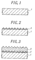
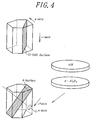
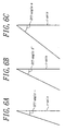
- Figs. 1-3 are cross sectional views showing successive steps of an embodiment of the method of manufacturing the substrate for a surface acoustic wave device according to the invention.
- a sapphire single crystal wafer 1 expressed by a composition of ⁇ -Al 2 O 3 is prepared.
- the sapphire single crystal wafer 1 has a diameter of two inches and a thickness of about 450 ⁇ m.
- an aluminum nitride or aluminum-gallium nitride buffer layer is deposited on the sapphire wafer 1, and an aluminum nitride single crystal layer is deposited on the buffer layer.
- the sapphire single crystal substrate 1 has an off-angled surface obtained by rotating an R(1-102) surface about a [11-20] axis by a given off-angle.
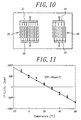
- Fig. 4 shows the R(1-102) surface as well as the [11-20] axis of the sapphire wafer 1, [11-20] axis being denoted by an a-axis.
- the R(1-102) surface of the sapphire single crystal wafer is rotated about the a-axis. In this case, the rotation may be performed in both directions, i.e. positive and negative directions as shown by arrows in Fig. 4.
- Fig. 5 is a schematic view for defining the direction of the rotation of the R-surface about the a-axis.
- a rotation in the clockwise direction is denoted as + direction and a rotation in the anti-clockwise direction is denoted as - direction.
- Fig. 5 there is also shown a c-axis.
- An angle between the c-axis and the R-surface is shown in Figs. 6A-6C.
- Fig. 6B illustrates a case of no or zero off-angle
- Fig. 6A shows a case in which the R-surface is rotated in the - direction
- Fig. 6C depicts a case in which the R-surface is rotated in the + direction.
- the R-surface is rotated in - direction to suppress effectively the generation of clacks.
- a buffer layer 2 consisting of a gallium nitride film is deposited on the off-angled surface of the sapphire single crystal wafer 1 by the metal organic chemical vapor deposition (MOCVD), said off-angled surface of the sapphire surface being obtained by rotating the R-surface about the a-axis in the - direction.
- MOCVD metal organic chemical vapor deposition
- a thickness of such a gallium nitride film 2 is expressed by an average thickness.
- the buffer layer 2 consisting of the gallium nitride film has an average thickness of 0.13 ⁇ m.
- the gallium nitride layer 2 has preferably an average thickness not less than 0.1 ⁇ m in order to suppress the formation of clacks.
- an aluminum nitride single crystal layer 3 is deposited on the gallium nitride layer 2 also by MOCVD.
- MOCVD metal-organic chemical vapor deposition
- the surface of the aluminum nitride single crystal layer 3 is polished into a smooth surface.
- a thickness of the thus polished aluminum nitride layer 3 is expressed as an average thickness.
- the surface of aluminum nitride single crystal layer 3 formed on the off angled surface of the sapphire single crystal substrate 1 is the R(1-210) rotated by an angle corresponding to the off-angle.
- this (1-210) surface of the aluminum nitride single crystal layer 3 is also shown.
- the aluminum nitride single crystal layer 3 has an average thickness of about 2.3 ⁇ m. According to the invention, in order to attain a desired surface acoustic wave property, it is preferable that an average thickness of the aluminum nitride single crystal layer 3 is not less than about 2 ⁇ m.
- a desired interdigital type electrode pattern is formed on the aluminum nitride single crystal layer 3 with the aid of the conventional method.
- the sapphire single crystal wafer 1 having the layers 2 and 3 and the interdigital electrode patter formed thereon is divided into chips by the conventional slicing technique. The thus obtained chips are placed in packages, given conducting wires are secured to electrodes, and finally the packages are sealed in an air-tight manner. In this manner, a surface acoustic wave device can be obtained on a mass production scale.
- the sapphire single crystal wafer 1 having the off-angled surface is introduced into a CVD apparatus and then is heated to a temperature of about 1000°C, while a hydrogen gas is introduced into the CVD apparatus to subject the sapphire wafer 1 to the hydrogen annealing for about thirty minutes.
- the CVD apparatus is maintained at a pressure of about 15 Torrs.
- the temperature of the sapphire single crystal wafer 1 is decreased to about 950°C, and after that an initial nitriding treatment is performed by introducing an ammonia (NH3) gas at a flow rate of 1-5 litters/min for about ten minutes into the CVD apparatus together with a carrier gas consisting of hydrogen or nitrogen.
- NH3 ammonia
- a trimethylgallium (TMG) gas and an ammonia gas are introduced into the CVD apparatus at flow rates of about 25 ⁇ mole/min and about 2 litters/min, respectively for about ten minutes to deposit gallium nitride to form the gallium nitride layer 2 having an average thickness of about 0.13 ⁇ m.
- a trimethylaluminum (TMA) gas and an ammonia gas are introduced into the CVD apparatus for one hundred and twenty minutes at flow rates of 30 ⁇ mole/min and 1-5 litters/min, respectively to deposit the aluminum nitride single crystal layer 3 with an average thickness of about 2.3 ⁇ m.
- TMG trimethylgallium
- an ammonia gas are introduced into the CVD apparatus for one hundred and twenty minutes at flow rates of 30 ⁇ mole/min and 1-5 litters/min, respectively to deposit the aluminum nitride single crystal layer 3 with an average thickness of about 2.3 ⁇ m.
- only the hydrogen carrier gas is supplied and the sapphire single crystal substrate
- the gallium nitride buffer layer 2 and the aluminum nitride single crystal layer 3 can be successively deposited without removing the sapphire wafer 1 from the CVD apparatus, and moreover the sapphire single crystal substrate is kept to a constant temperature, the manufacturing process is very simple.
- the sapphire single crystal substrate or wafer 1 having the off-angled surface which is obtained by rotating the R(1-102) surface about the [11-20] axis by a given off-angle.
- the rotation angle of the R(1-102) about the [11-20] axis is denoted on the horizontal axis, and the clack generation rate is represented on the vertical axis.
- the off-angle is changed within a range from +4° to -4°. As can be understood from Fig. 8, when the off-angle is zero, i.e.
- the clack generation rate amounts to a large value about 70%, and the clack generation rate is further increased when the R-surface is rotated in the + direction.
- the clack generation rate is decreased abruptly.
- the - rotation exceeds 2°, the clack generation rate becomes substantially zero.
- Fig. 9 is a graph showing a variation of the clack generation rate when an average thickness of the gallium nitride buffer layer 2 is changed.
- the gallium nitride buffer layer 2 is formed on the sapphire single crystal substrate 1 having the off-angle of -4°, and the aluminum nitride single crystal layer 3 having an average thickness of 2 ⁇ m is deposited.
- the clack generation rate is evaluated by the number of clacks induced in a three inch wafer.
- the gallium nitride buffer layer 2 when an average thickness of the gallium nitride buffer layer 2 is smaller than 0.1 ⁇ m, the practically obstacle number of clacks are induced, but when an average thickness of the gallium nitride buffer layer 2 is larger than 0.1 ⁇ m, the generation of clacks is extremely suppressed.
- an average thickness of the gallium nitride buffer layer 2 is larger than 0.2 ⁇ m, there is no remarkable change in the reduction of the clack generation rate, and therefore it is preferable that the gallium nitride buffer layer has an average thickness of 01-0.2 ⁇ m.
- Fig. 10 is a plan view showing an embodiment of the surface acoustic wave device according to the invention comprising the substrate explained above.
- the surface acoustic wave device is formed as a surface acoustic wave filter, which comprises a sapphire single crystal substrate, a gallium nitride buffer layer deposited on the sapphire substrate with an average thickness of 0.1 ⁇ m and an aluminum nitride single crystal layer deposited on buffer layer with an average thickness of 2.3 ⁇ m, and an electrode structure is deposited on the aluminum nitride single crystal layer.
- an input side transducer 23 is formed by regular type interdigital electrodes 21 and 22 whose adjacent electrode fingers are interdigitally crossed each other, and an output side transducer 26 is arranged to be separated from the input side transducer 21 by a predetermined distance, said output side transducer being also formed by regular type interdigital electrodes 24 and 25 whose adjacent electrode fingers are crossed with each other in an interdigital manner.
- the aluminum nitride single crystal layer on which the electrodes are deposited has a very high propagating velocity for a surface acoustic wave not lower than 5000 m/sec, and thus by suitably setting widths of electrode fingers and distances between adjacent electrode fingers, it is possible to realize the surface acoustic wave filter having a very high operation frequency of an order of GHz.
- Fig. 11 is a graph showing TCF (Temperature Coefficient of Frequency) at a center frequency of the surface acoustic wave device shown in Fig. 10.
- a designed center frequency is 2500 MHz and a wavelength ⁇ is 2.25 ⁇ m.
- TCF is theoretically expressed by (f-f 0 )/f 0 (ppm) , where f 0 is the center frequency.
- the surface acoustic wave device according to the invention can have TCF of -20 ppm/°C, which is close to a theoretical value.
- the buffer layer is consisting of the gallium nitride layer, but it may be consisting of an aluminum-gallium nitride (Al-Ga-N) layer.
- Al-Ga-N aluminum-gallium nitride
- a composition ratio between aluminum and gallium may be adjusted over a wide range by controlling flow rates of NH 3 , TMG and TMA during the MOCVD process.
- the composition of the aluminum-gallium nitride buffer layer may be changed in a direction of a thickness. For instance, a flow rate of TMG is gradually increased and at the same time a flow rate of TMA is gradually decreased.
- the effects obtained by the above embodiment can be equally obtained by using the aluminum-gallium (Al-Ga-N) nitride as the buffer layer.
- the sapphire single crystal wafer having a diameter of three inches use is made of the sapphire single crystal wafer having a diameter of three inches, but according to the invention a sapphire single crystal wafer having a diameter which is smaller or larger than three inches may be used.
- a sapphire single crystal wafer having a diameter not less than two inches it is preferable to use a sapphire single crystal wafer having a diameter not less than two inches.
- the surface acoustic wave device is realized as the surface acoustic wave filter having the regular type interdigital electrodes, but the surface acoustic wave filter may comprise any other type of electrodes or weighted electrodes. Further, the surface acoustic wave device may be realized as surface acoustic wave resonator or delay line.
- the aluminum nitride single crystal layer which has no clack, a sufficiently high electromechanical coupling coefficient K 2 , a sufficiently small TCF at the center frequency, and a high propagating velocity for the surface acoustic wave even if the sapphire single crystal wafer of not less than two inches is used. Therefore, surface acoustic wave devices having excellent property and an extremely high operation frequency can be realized at a low cost.
- the buffer layer can have a sufficiently large average thickness which can be controlled easily and accurately, and the deposition of the buffer layer can be performed at a high temperature. Therefore, the manufacturing process can be simplified and the manufacturing cost can be reduced.
- a sapphire single crystal wafer 11 having a diameter not less than two inches and having an off angled surface which is obtained by rotating an R (1-102) surface about a [11-20] axis in a negative direction by a given off-angle not less than 2° is introduced in a CVD apparatus. While the sapphire substrate is kept at a temperature about 950°C, a buffer layer made of gallium nitride or aluminum-gallium nitride is first deposited with an average thickness of 0.1-0.2 ⁇ m, and then a aluminum nitride single crystal layer is deposited with an average thickness not less than about 2 ⁇ m. The thus obtained aluminum nitride single crystal layer has not a significant amount of clacks, has an excellent piezoelectric property, and has a high propagating velocity.
Landscapes
- Physics & Mathematics (AREA)
- Acoustics & Sound (AREA)
- Surface Acoustic Wave Elements And Circuit Networks Thereof (AREA)
- Chemical Vapour Deposition (AREA)
- Crystals, And After-Treatments Of Crystals (AREA)
Applications Claiming Priority (6)
| Application Number | Priority Date | Filing Date | Title |
|---|---|---|---|
| JP31231698 | 1998-11-02 | ||
| JP31231698 | 1998-11-02 | ||
| JP31289298 | 1998-11-04 | ||
| JP31289298 | 1998-11-04 | ||
| JP11028538A JP2000201050A (ja) | 1998-11-02 | 1999-02-05 | 表面弾性波装置用基板およびその製造方法 |
| JP2853899 | 1999-02-05 |
Publications (2)
| Publication Number | Publication Date |
|---|---|
| EP0999640A2 true EP0999640A2 (fr) | 2000-05-10 |
| EP0999640A3 EP0999640A3 (fr) | 2000-09-27 |
Family
ID=27286232
Family Applications (1)
| Application Number | Title | Priority Date | Filing Date |
|---|---|---|---|
| EP99121666A Withdrawn EP0999640A3 (fr) | 1998-11-02 | 1999-11-02 | Dispositif à ondes acoustiques de surface, substrat correspondant et procédé pour la fabrication du substrat |
Country Status (3)
| Country | Link |
|---|---|
| US (1) | US6342748B1 (fr) |
| EP (1) | EP0999640A3 (fr) |
| JP (1) | JP2000201050A (fr) |
Cited By (5)
| Publication number | Priority date | Publication date | Assignee | Title |
|---|---|---|---|---|
| EP1197996A2 (fr) * | 2000-10-13 | 2002-04-17 | Ngk Insulators, Ltd. | Plaquette épitaxiale du type groupe III-nitrure et son utilisation |
| KR100388011B1 (ko) * | 2000-01-17 | 2003-06-18 | 삼성전기주식회사 | GaN박막 SAW필터 및 이를 제조하는 방법 |
| US7220314B2 (en) * | 2002-03-14 | 2007-05-22 | The Circle For The Promotion Of Science And Engineering | Single crystalline aluminum nitride film, method of forming the same, base substrate for group III element nitride film, light emitting device and surface acoustic wave device |
| US7338555B2 (en) * | 2003-09-12 | 2008-03-04 | Tokuyama Corporation | Highly crystalline aluminum nitride multi-layered substrate and production process thereof |
| CN110176915A (zh) * | 2018-02-19 | 2019-08-27 | 日本电波工业株式会社 | 弹性表面波装置 |
Families Citing this family (16)
| Publication number | Priority date | Publication date | Assignee | Title |
|---|---|---|---|---|
| US6972436B2 (en) * | 1998-08-28 | 2005-12-06 | Cree, Inc. | High voltage, high temperature capacitor and interconnection structures |
| US7067176B2 (en) * | 2000-10-03 | 2006-06-27 | Cree, Inc. | Method of fabricating an oxide layer on a silicon carbide layer utilizing an anneal in a hydrogen environment |
| US7022378B2 (en) * | 2002-08-30 | 2006-04-04 | Cree, Inc. | Nitrogen passivation of interface states in SiO2/SiC structures |
| US20060008676A1 (en) * | 2004-07-07 | 2006-01-12 | General Electric Company | Protective coating on a substrate and method of making thereof |
| JP5097338B2 (ja) * | 2005-05-31 | 2012-12-12 | 株式会社日立メディアエレクトロニクス | 圧電薄膜弾性波素子、圧電薄膜弾性波素子を用いた情報処理装置、及び圧電薄膜弾性波素子の製造方法 |
| US7727904B2 (en) | 2005-09-16 | 2010-06-01 | Cree, Inc. | Methods of forming SiC MOSFETs with high inversion layer mobility |
| JP2007103774A (ja) * | 2005-10-06 | 2007-04-19 | Showa Denko Kk | Iii族窒化物半導体積層構造体およびその製造方法 |
| JP5004597B2 (ja) * | 2006-03-06 | 2012-08-22 | シャープ株式会社 | 窒化物半導体発光素子および窒化物半導体発光素子の製造方法 |
| JP5307975B2 (ja) * | 2006-04-21 | 2013-10-02 | 日立電線株式会社 | 窒化物系半導体自立基板及び窒化物系半導体発光デバイス用エピタキシャル基板 |
| JP2008214132A (ja) * | 2007-03-05 | 2008-09-18 | Univ Of Tokushima | Iii族窒化物半導体薄膜、iii族窒化物半導体発光素子およびiii族窒化物半導体薄膜の製造方法 |
| DE102007037502B4 (de) * | 2007-08-08 | 2014-04-03 | Epcos Ag | Bauelement mit reduziertem Temperaturgang |
| US7977224B2 (en) * | 2008-12-03 | 2011-07-12 | The United States Of America As Represented By The Secretary Of The Army | Method using multiple layer annealing cap for fabricating group III-nitride semiconductor device structures and devices formed thereby |
| JP2012033708A (ja) * | 2010-07-30 | 2012-02-16 | Sumitomo Electric Ind Ltd | 半導体装置の製造方法 |
| US9984894B2 (en) | 2011-08-03 | 2018-05-29 | Cree, Inc. | Forming SiC MOSFETs with high channel mobility by treating the oxide interface with cesium ions |
| US10340416B2 (en) * | 2016-02-26 | 2019-07-02 | Riken | Crystal substrate, ultraviolet light-emitting device, and manufacturing methods therefor |
| CN112038217B (zh) * | 2020-09-11 | 2021-07-16 | 广东广纳芯科技有限公司 | AlN单晶薄膜生长方法及具有该薄膜的声表面波谐振器 |
Family Cites Families (10)
| Publication number | Priority date | Publication date | Assignee | Title |
|---|---|---|---|---|
| CA2037198C (fr) * | 1990-02-28 | 1996-04-23 | Toyoda Gosei Co., Ltd. | Dispositif luminescent utilisant un semiconducteur du groupe nitrure de gallium |
| JP2934337B2 (ja) | 1991-04-23 | 1999-08-16 | 旭化成工業株式会社 | 窒化ガリウム系半導体発光素子材料 |
| JP2795294B2 (ja) | 1991-10-12 | 1998-09-10 | 日亜化学工業株式会社 | 窒化ガリウムアルミニウム半導体の結晶成長方法。 |
| US5278435A (en) * | 1992-06-08 | 1994-01-11 | Apa Optics, Inc. | High responsivity ultraviolet gallium nitride detector |
| US5598014A (en) * | 1995-02-28 | 1997-01-28 | Honeywell Inc. | High gain ultraviolet photoconductor based on wide bandgap nitrides |
| US5650198A (en) * | 1995-08-18 | 1997-07-22 | The Regents Of The University Of California | Defect reduction in the growth of group III nitrides |
| JPH09312546A (ja) | 1996-05-22 | 1997-12-02 | Kyocera Corp | 弾性表面波装置 |
| JP3321369B2 (ja) | 1996-09-27 | 2002-09-03 | 日本碍子株式会社 | 表面弾性波装置およびその基板およびその製造方法 |
| JP3813740B2 (ja) * | 1997-07-11 | 2006-08-23 | Tdk株式会社 | 電子デバイス用基板 |
| US6051849A (en) * | 1998-02-27 | 2000-04-18 | North Carolina State University | Gallium nitride semiconductor structures including a lateral gallium nitride layer that extends from an underlying gallium nitride layer |
-
1999
- 1999-02-05 JP JP11028538A patent/JP2000201050A/ja active Pending
- 1999-11-01 US US09/431,398 patent/US6342748B1/en not_active Expired - Fee Related
- 1999-11-02 EP EP99121666A patent/EP0999640A3/fr not_active Withdrawn
Cited By (7)
| Publication number | Priority date | Publication date | Assignee | Title |
|---|---|---|---|---|
| KR100388011B1 (ko) * | 2000-01-17 | 2003-06-18 | 삼성전기주식회사 | GaN박막 SAW필터 및 이를 제조하는 방법 |
| US6583690B2 (en) * | 2000-01-17 | 2003-06-24 | Samsung Electro-Mechanics Co., Ltd. | Saw filter manufactured by using GaN single crystal thin film, and manufacturing method therefore |
| EP1197996A2 (fr) * | 2000-10-13 | 2002-04-17 | Ngk Insulators, Ltd. | Plaquette épitaxiale du type groupe III-nitrure et son utilisation |
| US7220314B2 (en) * | 2002-03-14 | 2007-05-22 | The Circle For The Promotion Of Science And Engineering | Single crystalline aluminum nitride film, method of forming the same, base substrate for group III element nitride film, light emitting device and surface acoustic wave device |
| US7338555B2 (en) * | 2003-09-12 | 2008-03-04 | Tokuyama Corporation | Highly crystalline aluminum nitride multi-layered substrate and production process thereof |
| CN110176915A (zh) * | 2018-02-19 | 2019-08-27 | 日本电波工业株式会社 | 弹性表面波装置 |
| CN110176915B (zh) * | 2018-02-19 | 2023-03-24 | Ndk声表滤波器股份有限公司 | 弹性表面波装置 |
Also Published As
| Publication number | Publication date |
|---|---|
| JP2000201050A (ja) | 2000-07-18 |
| US6342748B1 (en) | 2002-01-29 |
| EP0999640A3 (fr) | 2000-09-27 |
Similar Documents
| Publication | Publication Date | Title |
|---|---|---|
| EP0999640A2 (fr) | Dispositif à ondes acoustiques de surface, substrat correspondant et procédé pour la fabrication du substrat | |
| US6183555B1 (en) | Surface acoustic wave device, substrate therefor, and method of manufacturing the substrate | |
| US5401544A (en) | Method for manufacturing a surface acoustic wave device | |
| CN111801890B (zh) | 多个层系统、制造方法以及在多个层系统上形成的saw设备 | |
| KR100859674B1 (ko) | 압전막을 갖는 장치를 제조하는 방법 | |
| US6312568B2 (en) | Two-step AIN-PVD for improved film properties | |
| EP0669412A1 (fr) | Substrat pour film mince de nitrure d'aluminium et son procédé de production | |
| US20080303378A1 (en) | Surface acoustic wave (saw) devices based on cubic boron nitride/diamond composite structures | |
| CN115259073B (zh) | 一种mems单片集成电路及其制备方法 | |
| US6710513B2 (en) | Surface acoustic wave device and substrate thereof | |
| EP3920417A2 (fr) | Substrat composite pour un dispositif à onde acoustique de surface et son procédé de fabrication | |
| JP2000201050A5 (fr) | ||
| CN115694391A (zh) | 复合衬底的制造方法、复合衬底及声表面波滤波器 | |
| US7213322B2 (en) | Method for manufacturing surface acoustic wave device | |
| EP3971999A1 (fr) | Dispositif piézoélectrique, son procédé de fabrication, dispositif d'onde acoustique de surface et dispositif de résonance à couche mince piézoélectrique | |
| EP0534252B1 (fr) | Dispositif à ondes acoustiques de surface | |
| JPH0220910A (ja) | 弾性表面波ディバイス | |
| KR20100082541A (ko) | 표면탄성파 소자 | |
| US7615910B1 (en) | High frequency surface acoustic wave device | |
| CN116318033A (zh) | 通信器件、传感器件、表面声波谐振器及其制作方法 | |
| US6800135B2 (en) | ZnO/sapphire substrate and method for manufacturing the same | |
| JP2000332314A (ja) | 圧電体基板の製造方法 | |
| JPH09312546A (ja) | 弾性表面波装置 | |
| US20250192749A1 (en) | Piezoelectric-on-insulator (poi) substrate and method for producing a piezoelectric-on-insulator (poi) substrate | |
| JPH07326943A (ja) | 弾性表面波装置 |
Legal Events
| Date | Code | Title | Description |
|---|---|---|---|
| PUAI | Public reference made under article 153(3) epc to a published international application that has entered the european phase |
Free format text: ORIGINAL CODE: 0009012 |
|
| AK | Designated contracting states |
Kind code of ref document: A2 Designated state(s): DE FR GB |
|
| AX | Request for extension of the european patent |
Free format text: AL;LT;LV;MK;RO;SI |
|
| PUAL | Search report despatched |
Free format text: ORIGINAL CODE: 0009013 |
|
| AK | Designated contracting states |
Kind code of ref document: A3 Designated state(s): AT BE CH CY DE DK ES FI FR GB GR IE IT LI LU MC NL PT SE |
|
| AX | Request for extension of the european patent |
Free format text: AL;LT;LV;MK;RO;SI |
|
| 17P | Request for examination filed |
Effective date: 20010226 |
|
| AKX | Designation fees paid |
Free format text: DE FR GB |
|
| 17Q | First examination report despatched |
Effective date: 20040722 |
|
| STAA | Information on the status of an ep patent application or granted ep patent |
Free format text: STATUS: THE APPLICATION IS DEEMED TO BE WITHDRAWN |
|
| 18D | Application deemed to be withdrawn |
Effective date: 20041202 |