EP1000741A2 - Drucker für elektronisches Papier - Google Patents
Drucker für elektronisches Papier Download PDFInfo
- Publication number
- EP1000741A2 EP1000741A2 EP99120725A EP99120725A EP1000741A2 EP 1000741 A2 EP1000741 A2 EP 1000741A2 EP 99120725 A EP99120725 A EP 99120725A EP 99120725 A EP99120725 A EP 99120725A EP 1000741 A2 EP1000741 A2 EP 1000741A2
- Authority
- EP
- European Patent Office
- Prior art keywords
- electronic paper
- drum
- head
- pixel electrodes
- printer according
- Prior art date
- Legal status (The legal status is an assumption and is not a legal conclusion. Google has not performed a legal analysis and makes no representation as to the accuracy of the status listed.)
- Granted
Links
- 230000005684 electric field Effects 0.000 claims description 78
- 239000010409 thin film Substances 0.000 claims description 63
- 239000002245 particle Substances 0.000 claims description 35
- 239000002775 capsule Substances 0.000 claims description 30
- 239000003086 colorant Substances 0.000 claims description 11
- 239000011159 matrix material Substances 0.000 claims description 8
- 238000001962 electrophoresis Methods 0.000 abstract description 4
- 238000000034 method Methods 0.000 description 19
- 239000003094 microcapsule Substances 0.000 description 14
- 238000010586 diagram Methods 0.000 description 13
- 239000007788 liquid Substances 0.000 description 12
- 239000000758 substrate Substances 0.000 description 5
- 230000015572 biosynthetic process Effects 0.000 description 4
- 230000005484 gravity Effects 0.000 description 4
- GWEVSGVZZGPLCZ-UHFFFAOYSA-N Titan oxide Chemical compound O=[Ti]=O GWEVSGVZZGPLCZ-UHFFFAOYSA-N 0.000 description 3
- 239000011230 binding agent Substances 0.000 description 3
- 230000002708 enhancing effect Effects 0.000 description 3
- 230000001747 exhibiting effect Effects 0.000 description 3
- 230000000694 effects Effects 0.000 description 2
- CYTYCFOTNPOANT-UHFFFAOYSA-N Perchloroethylene Chemical compound ClC(Cl)=C(Cl)Cl CYTYCFOTNPOANT-UHFFFAOYSA-N 0.000 description 1
- 239000004698 Polyethylene Substances 0.000 description 1
- 239000004372 Polyvinyl alcohol Substances 0.000 description 1
- PYKYMHQGRFAEBM-UHFFFAOYSA-N anthraquinone Natural products CCC(=O)c1c(O)c2C(=O)C3C(C=CC=C3O)C(=O)c2cc1CC(=O)OC PYKYMHQGRFAEBM-UHFFFAOYSA-N 0.000 description 1
- 150000004056 anthraquinones Chemical class 0.000 description 1
- 239000000919 ceramic Substances 0.000 description 1
- 239000012769 display material Substances 0.000 description 1
- 230000006870 function Effects 0.000 description 1
- 239000002184 metal Substances 0.000 description 1
- 230000010355 oscillation Effects 0.000 description 1
- -1 polyethylene Polymers 0.000 description 1
- 229920000573 polyethylene Polymers 0.000 description 1
- 229920002451 polyvinyl alcohol Polymers 0.000 description 1
- 239000011347 resin Substances 0.000 description 1
- 229920005989 resin Polymers 0.000 description 1
- 239000002904 solvent Substances 0.000 description 1
- 229950011008 tetrachloroethylene Drugs 0.000 description 1
- 238000011144 upstream manufacturing Methods 0.000 description 1
- 239000002699 waste material Substances 0.000 description 1
Images


Classifications
-
- B—PERFORMING OPERATIONS; TRANSPORTING
- B41—PRINTING; LINING MACHINES; TYPEWRITERS; STAMPS
- B41J—TYPEWRITERS; SELECTIVE PRINTING MECHANISMS, i.e. MECHANISMS PRINTING OTHERWISE THAN FROM A FORME; CORRECTION OF TYPOGRAPHICAL ERRORS
- B41J3/00—Typewriters or selective printing or marking mechanisms characterised by the purpose for which they are constructed
- B41J3/407—Typewriters or selective printing or marking mechanisms characterised by the purpose for which they are constructed for marking on special material
- B41J3/4076—Typewriters or selective printing or marking mechanisms characterised by the purpose for which they are constructed for marking on special material printing on rewritable, bistable "electronic paper" by a focused electric or magnetic field
-
- B—PERFORMING OPERATIONS; TRANSPORTING
- B41—PRINTING; LINING MACHINES; TYPEWRITERS; STAMPS
- B41J—TYPEWRITERS; SELECTIVE PRINTING MECHANISMS, i.e. MECHANISMS PRINTING OTHERWISE THAN FROM A FORME; CORRECTION OF TYPOGRAPHICAL ERRORS
- B41J2/00—Typewriters or selective printing mechanisms characterised by the printing or marking process for which they are designed
- B41J2/435—Typewriters or selective printing mechanisms characterised by the printing or marking process for which they are designed characterised by selective application of radiation to a printing material or impression-transfer material
-
- G—PHYSICS
- G02—OPTICS
- G02F—OPTICAL DEVICES OR ARRANGEMENTS FOR THE CONTROL OF LIGHT BY MODIFICATION OF THE OPTICAL PROPERTIES OF THE MEDIA OF THE ELEMENTS INVOLVED THEREIN; NON-LINEAR OPTICS; FREQUENCY-CHANGING OF LIGHT; OPTICAL LOGIC ELEMENTS; OPTICAL ANALOGUE/DIGITAL CONVERTERS
- G02F1/00—Devices or arrangements for the control of the intensity, colour, phase, polarisation or direction of light arriving from an independent light source, e.g. switching, gating or modulating; Non-linear optics
- G02F1/01—Devices or arrangements for the control of the intensity, colour, phase, polarisation or direction of light arriving from an independent light source, e.g. switching, gating or modulating; Non-linear optics for the control of the intensity, phase, polarisation or colour
- G02F1/165—Devices or arrangements for the control of the intensity, colour, phase, polarisation or direction of light arriving from an independent light source, e.g. switching, gating or modulating; Non-linear optics for the control of the intensity, phase, polarisation or colour based on translational movement of particles in a fluid under the influence of an applied field
- G02F1/166—Devices or arrangements for the control of the intensity, colour, phase, polarisation or direction of light arriving from an independent light source, e.g. switching, gating or modulating; Non-linear optics for the control of the intensity, phase, polarisation or colour based on translational movement of particles in a fluid under the influence of an applied field characterised by the electro-optical or magneto-optical effect
- G02F1/167—Devices or arrangements for the control of the intensity, colour, phase, polarisation or direction of light arriving from an independent light source, e.g. switching, gating or modulating; Non-linear optics for the control of the intensity, phase, polarisation or colour based on translational movement of particles in a fluid under the influence of an applied field characterised by the electro-optical or magneto-optical effect by electrophoresis
-
- G—PHYSICS
- G02—OPTICS
- G02F—OPTICAL DEVICES OR ARRANGEMENTS FOR THE CONTROL OF LIGHT BY MODIFICATION OF THE OPTICAL PROPERTIES OF THE MEDIA OF THE ELEMENTS INVOLVED THEREIN; NON-LINEAR OPTICS; FREQUENCY-CHANGING OF LIGHT; OPTICAL LOGIC ELEMENTS; OPTICAL ANALOGUE/DIGITAL CONVERTERS
- G02F1/00—Devices or arrangements for the control of the intensity, colour, phase, polarisation or direction of light arriving from an independent light source, e.g. switching, gating or modulating; Non-linear optics
- G02F1/01—Devices or arrangements for the control of the intensity, colour, phase, polarisation or direction of light arriving from an independent light source, e.g. switching, gating or modulating; Non-linear optics for the control of the intensity, phase, polarisation or colour
- G02F1/165—Devices or arrangements for the control of the intensity, colour, phase, polarisation or direction of light arriving from an independent light source, e.g. switching, gating or modulating; Non-linear optics for the control of the intensity, phase, polarisation or colour based on translational movement of particles in a fluid under the influence of an applied field
- G02F1/1675—Constructional details
- G02F1/16757—Microcapsules
Definitions
- This invention relates to a printer for electronic paper.
- segments in the display are configured by a plurality of micro-capsules that employ electrophoresis, such that, by applying a voltage to a target segment, the color of that segment changes, either partially or entirely.
- An object of the present invention is to provide an electronic paper printer capable of describing display patterns properly and definitely on rewritable electronic paper.
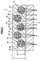
- Fig. 1 is a side elevation representing a first embodiment of the electronic paper printer of the present invention.
- An electronic paper printer 1 indicated in Fig. 1 is an apparatus for describing (printing) prescribed display patterns displays such as text characters, numbers, and graphics pictures on electronic paper 2 that will be described subsequently.
- This electronic paper printer 1 has a describing head (first head) 3 for describing display patterns on the electronic paper 2, an erasing head (second head) 4 for erasing display patterns that have been described on the electronic paper 2, a drive mechanism (not shown) for driving the describing head 3 and erasing head 4 so that they revolve, and a conveyor mechanism (not shown) for conveying the electronic paper 2.
- the direction of arrow A in Fig. 1 is the direction the electronic paper 2 is conveyed in.
- Fig. 2 is a cross-sectional diagram of an example configuration for the electronic paper 2.
- Fig. 3 is a cross-sectional diagram of a micro-capsule in the electronic paper diagrammed in Fig. 2.
- the electronic paper 2 diagrammed in Fig. 2 constitutes display means (display media) capable of rewriting and erasing display patterns using electrophoresis.
- This electronic paper 2 comprises paper (a sheet-form base layer exhibiting flexibility) 21 and an electronic ink layer 22 formed on the paper 21.
- the surface on the upper side of this electronic ink layer 22, as diagrammed in Fig. 2, is a display surface 20 whereon display patterns are displayed.
- the electronic ink layer 22 comprises a transparent binder 23 exhibiting light transmissivity and a plurality of micro-capsules 24 which are fixed in a state wherein they are uniformly dispersed in the binder 23.
- the thickness a of the electronic ink layer 22 be from 1.5 to 2 times the outer diameter (i.e. diameter) b of the micro-capsules 24.
- Polyvinyl alcohol or the like can be used as the binder 23.
- each micro-capsule 24 has a main capsule body 25 that is shaped as a hollow sphere and exhibits light transmissivity.
- the interior of this main capsule body 25 is filled with a liquid solvent 26.
- this liquid 26 is dispersed a plurality of charged particles 27 having negative charges.
- Each charged particle 27 comprises a nucleus 28 and a covering layer 29 that covers the nucleus 28.
- the colors of the charged particles 27 and the liquid 26 are set so as to be mutually different. If the color of the charged particles 27 is made white, for example, the color of the liquid 26 might be made blue, red, green, or black.
- the charged particles 27 move, inside the main capsule body 25, in a direction opposite the direction of the electric field.
- an external electric field i.e. electric field
- a positively charged electrode is positioned above the micro-capsule 24 (display surface 20 side), as diagrammed in Fig. 3, an electric field is produced that is directed toward the bottom in Fig. 3, as a consequence whereof the charged particles 27 move (float up) to the upper side, as diagrammed in Fig. 3, inside the main capsule body 25. Due to these charged particles 27, the color of the upper side of the micro-capsule 24, as diagrammed in Fig. 3, will turn white.
- a negatively charged electrode is positioned on the upper side of the micro-capsule 24, as diagrammed in Fig. 3, an electric field will be produced that is directed toward the upper side, in Fig. 3.
- the charged particles 27 will move down (sink) toward the lower side in the main capsule body 25, as diagrammed in Fig. 3.
- the liquid 26 is positioned on the upper side in the main capsule body 25, as diagrammed in Fig. 3, wherefore, if the color of the liquid is blue, the color of the upper side of the micro-capsule 24, as diagrammed in Fig. 3, will become blue.
- micro-capsules 24 are configured such that the specific gravity of the liquid 26 and the specific gravity of the charged particles 27 become equal.
- the charged particles 27, after moving either up or down, as diagrammed in Fig. 3, can remain in a certain position for a long period of time, even if the electric field disappears, the color on the upper side of the micro-capsule 24, as diagrammed in Fig. 3, can be maintained white, and the color of the liquid can be maintained blue, for example, for a long time. In other words, the display on the electronic paper 2 can be maintained for a long period of time.
- the thickness d of the covering layer 29, for example may be adjusted.
- the outer diameter b of the micro-capsule 24 should be 180 ⁇ m or less, with 10 to 20 ⁇ m or so being preferable.
- TiO 2 rutile structure or the like, for example, can be used for the nuclei 28 of the charged particles 27.
- a polyethylene or the like, for example, can be used for the covering layer 29 of the charged particles 27.
- a solution can be used wherein an anthraquinone-based dye is dissolved in ethylene tetrachloride and isoparaffin, for example.
- the describing head 3 is configured by a pair of drums 31 and 32 supported so that they can freely turn.
- the outer diameter of the drum 31 and the outer diameter of the drum 32 are set so as to be identical.
- the outer diameter of the drums 31 and 32 is not particularly limited, but 3 to 30 cm or so is desirable.
- the outer diameters of the drums 31 and 32 By making the outer diameters of the drums 31 and 32 large, the area of contact between the drums 31 and 32 and the electronic paper 2 can be increased, thereby enhancing the display pattern describing speed.
- drums 31 and 32 have axes (turning axes 312 and 322), respectively, which are mutually parallel, and the drums 31 and 32 are positioned so that the distance between the outer circumferential surfaces thereof is a prescribed distance.
- These drums 31 and 32 are also positioned so that the drum 31 is on the upper side, as diagrammed in Fig. 1, that is, on the electronic ink layer 22 side of the electronic paper 2, and so that the drum 32 is on the lower side, as diagrammed in Fig. 1, that is, on the paper 21 side of the electronic paper 2.
- the interval between the outer circumferential surface of the drum 31 and the outer circumferential surface of the drum 32 is set so that the electronic paper 2 can pass between the drum 31 and the drum 32, and so that the drum 31 and the drum 32 can apply pressure and electric fields on the electronic paper 2 as sufficient and as necessary.
- the drum 31 has a cylindrical drum body 311. On the outer circumferential surface of this drum body 311 is deployed a circuit board 313 comprising a plurality of pixel electrodes (upper electrodes). This circuit board 313 will be described in detail subsequently.
- the drum 32 meanwhile, has a cylindrical drum body 321. On the outer circumferential surface of this drum body 321 is deployed a common electrode (lower electrode) 323.
- Fig. 4 is a diagram (block diagram) which represents in model form the condition wherein the circuit board 313 is deployed.
- the direction of arrow A in Fig. 4 is the direction in which the electronic paper 2 is conveyed.
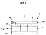
- Fig. 5 is a side elevation representing one pixel in the describing head 3.
- the direction of arrow A in Fig. 5 is the direction in which the electronic paper 2 is conveyed.
- the circuit board 313 has a substrate 61 formed of a resin exhibiting flexibility (elasticity).
- a plurality of square pixel electrodes 64 deployed (arrayed) in a matrix arrangement a plurality of thin film transistors (TFTs) (switching elements) 65 for switching the pixel electrodes 64 between conducting and non-conducting states, respectively, a gate driver 62 for applying voltages (signals) to the gates of the thin film transistors 65, a source driver 63 for applying voltages (signals) to the sources of the thin film transistors 65, a plurality of gate lines 621 that extend laterally, as diagrammed in Fig. 4, and a plurality of source lines 631 that extend vertically, as diagrammed in Fig. 4.
- TFTs thin film transistors
- Each pixel electrode 64 corresponds to one pixel (bit).
- pitch of the pixel electrodes 64 there is no particular limitation on the pitch of the pixel electrodes 64, but a pitch of 500 to 5000 dpi (dots per inch) or so is desirable.
- the shape of the pixel electrodes 64 is not limited to a square shape.
- the pattern in which the pixel electrodes 64 are arrayed is not limited to a matrix arrangement. There is no reason why the pixel electrodes 64 may not be deployed in a delta arrangement, for example.
- the uppermost laterally oriented array is called the "first row” and the Nth laterally oriented array from the top is called the "Nth row.”
- the leftmost vertically oriented array is called the "first column” and the Nth vertically oriented array from the left side is called the "Nth column.”
- each of the plurality of gate lines 621 that extend laterally, as diagrammed in Fig. 4.
- Each of the thin film transistors 65 is connected to a corresponding gate line 621.
- Each of the sources of the thin film transistors 65 is connected to a corresponding source line 631, and each of the drains of the thin film transistors 65 is connected to a corresponding pixel electrode 64.
- the gate driver 62 sequentially scans the gate lines 621 one row (line) at a time.
- To scan the Nth row gate line 621 for example, means to apply a voltage (scan voltage) precisely during a scanning time (time) t to the gates of all of the thin film transistors 65 in the Nth row, and [thus] turn on all of the thin film transistors 65 (i.e. the gates of the thin film transistors 65) in the Nth row for precisely the scanning time t.
- the role of the gate driver 62 is to sequentially scan the Nth row, and then the N+1'th row, and then the N+2'th row, that is, to sequentially turn on all of the thin film transistors 65 in each of the rows, in row units (i.e. one row at a time), for precisely the scanning time t.
- the source driver 63 is also called a data line drive circuit. This is a circuit that applies a voltage corresponding to printing information (information indicating a display pattern) to the pixel electrodes 64 via the source lines 631 and the thin film transistors 65 when a scanning voltage is applied to a prescribed gate line 621, that is, when all of the thin film transistors 65 in a prescribed row are turned on.
- a scanning voltage is applied to a prescribed gate line 621, the voltage noted above is applied to the prescribed source line 631, so that the corresponding pixel electrode 64 conducts.
- a negative voltage at a prescribed level can be applied to the corresponding pixel electrode 64, for example, and, as diagrammed in Fig. 5, that pixel electrode 64 can be given a negative charge, for example.
- the level of the voltage applied between the pixel electrode 64 noted above and the common electrode 323 (that is, the potential difference between that pixel electrode 64 and the common electrode 323) is not particularly limited, but, in terms of absolute values, a voltage of 10 volts or higher is desirable, and 20 volts or higher is even more preferable.
- the drives for the thin film transistors 65 noted earlier are controlled, respectively, by control means 7 via the gate driver 62 and the source driver 63.
- the control means 7 are ordinarily configured by an integrated circuit comprising a logic circuit and a memory circuit.
- the control means 7 control, in addition to the thin film transistors 65, the thin film transistors 65, etc., on the drum 41 of the erasing head 4 (described subsequently), and also the entire electronic paper printer 1.
- circuit board 313 on the outer circumferential surface of the drum body 311, as described earlier, be performed as described below, for example.
- a circuit unit comprising a thin film transistor array and pixel electrode array, etc., as described in the foregoing, is formed on a prescribed substrate (not shown), and this is then peeled away from the substrate by a prescribed method and transferred to the substrate 61. Thus is obtained the circuit board 313.
- the Japanese Patent Kokai No. H10-125930/1998 for which filing was made by the present applicant may be referenced.
- this circuit board 313 is wrapped about and fixed to the outer circumferential surface of the drum body 311.
- the erasing head 4 is deployed on the right side (in Fig. 1) of the describing head 3 (i.e. on the upstream side thereof as respecting the direction of conveyance of the electronic paper 2), separated from the describing head 3 by a prescribed distance.
- This erasing head 4 similarly to the describing head 3 described earlier, is configured by a pair of drums 41 and 42 that are supported so that they turn freely.
- the outer diameters of the drum 41 and the drum 42 are set equal to the outer diameters of the drum 31 and drum 32 of the describing head 3 described earlier (the outer diameter of the drum 41 and the outer diameter of the drum 42 also being set equal).
- drums 41 and 42 There is no particular limitation on the outer diameter of the drums 41 and 42, but, as with the drums 31 and 32 described earlier, a diameter of 3 to 30 cm or so is desirable.
- the outer diameters of the drums 41 and 42 By making the outer diameters of the drums 41 and 42 large, the area of contact between the drums 41 and 42 and the electronic paper 2 can be increased, thereby enhancing the display pattern erasing speed.
- drums 41 and 42 have axes (turning axes 412 and 422), respectively, which are mutually parallel, and the drums 41 and 42 are positioned so that the distance between the outer circumferential surfaces thereof is a prescribed distance, similarly to the describing head 3 described earlier.
- These drums 41 and 42 are also positioned, similarly to the describing head 3 described earlier, so that the drum 41 is on the upper side, as diagrammed in Fig. 1, that is, on the electronic ink layer 22 side of the electronic paper 2, and so that the drum 42 is on the lower side, as diagrammed in Fig. 1, that is, on the paper 21 side of the electronic paper 2.
- the drum 41 has a cylindrical drum body 411. On the outer circumferential surface of this drum body 411 is deployed a circuit board 413 comprising a plurality of pixel electrodes (upper electrodes) 64, as in the describing head 3 described earlier.
- This circuit board 413 is like the circuit board 313 in the describing head 3 described earlier, wherefore the description thereof will be abridged.
- the drum 42 meanwhile, has a cylindrical drum body 421. On the outer circumferential surface of this drum body 421 is deployed a common electrode (lower electrode) 423.
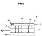
- Fig. 6 is a side elevation of one pixel in the erasing head 4.
- the direction of arrow A in Fig. 6 is the direction in which the electronic paper 2 is conveyed.
- the gate driver 62 sequentially scans the gate lines 621 one row (line) at a time (cf. Fig. 4).
- To scan the Nth row gate line 621 for example, means to apply a voltage (scan voltage) precisely during a scanning time (time) t to the gates of all of the thin film transistors 65 in the Nth row, and [thus] turn on all of the thin film transistors 65 (i.e. the gates of the thin film transistors 65) in the Nth row for precisely the scanning time t.
- the role of the gate driver 62 is to sequentially scan the Nth row, and then the N+1'th row, and then the N+2'th row, that is, to sequentially turn on all of the thin film transistors 65 in each of the rows, in row units (i.e. one row at a time), for precisely the scanning time t.
- the source driver 63 is also called a data line drive circuit. This is a circuit that applies a voltage to the pixel electrodes 64 via the source lines 631 and the thin film transistors 65 when a scanning voltage is applied to a prescribed gate line 621, that is, when all of the thin film transistors in a prescribed row are turned on.
- the level of the voltage applied between the pixel electrode 64 noted above and the common electrode 423 (that is, the potential difference between that pixel electrode 64 and the common electrode 423) is not particularly limited, but, in terms of absolute values, a voltage of 10 volts or higher is desirable, and 20 volts or higher is even more preferable.
- circuit board 413 on the outer circumferential surface of the drum body 411 described in the foregoing should be performed using the same method as for forming the circuit board 313 to the outer circumferential surface of the drum body 311 as described earlier.
- the drum 31 of the describing head 3 turns clockwise, as shown in Fig. 1, a prescribed number of revolutions (turning speed), while the drum 32 turns counterclockwise, as shown in Fig. 1, the same number of revolutions as the drum 31.
- This turning is performed by a drive mechanism.
- the drum 41 of the erasing head 4 turns clockwise, as shown in Fig. 1, the same number of revolutions as the drum 31, while the drum 42 turns counterclockwise, as shown in Fig. 1, the same number of revolutions as the drum 41.
- This turning is likewise performed by a drive mechanism.
- the electronic paper 2 is conveyed by the conveyor mechanism from the left side, as shown in Fig. 1, to the erasing head 4.
- the control means 7 drive the gate driver 62, scan all of the thin film transistors 65 in the erasing head 4, and turn them on, one row at a time.
- control means 7 also drives the source driver 63, and outputs the same electrical potential to all of the source lines 631.
- a positive voltage for example, at a prescribed level, is applied to all of the pixel electrodes 64. And, if the potential on the common electrode 423 has been set at 0 volts, electric fields are formed from the corresponding pixel electrodes 64 toward the common electrode 423.
- the electronic paper 2 is held between the drum 41 and the drum 42 and carried along in the direction of arrow A. That is, the electronic paper 2, from the leading end (the part on the left in Fig. 1), passes successively between the drums 41 and the drum 42. When this happens, the electronic paper 2 is subjected to prescribed pressures and placed in the electric fields described earlier (i.e. subjected to those electric fields), sequentially from the leading end, by the drum 41 and the drum 42.
- the charged particles 27 in the electronic paper 2 placed in the electric field as noted above move to the upper side, as shown in Fig. 7, in the main capsule units 25, respectively, due to that electric field.
- These charged particles 27 cause the display surface 20 of the electronic paper 2 corresponding thereto to turn white.
- the electronic paper 2 is carried along by the drum 41 and the drum 42 in the direction of arrow A and thereby conveyed to the describing head 3.
- control means 7 drive the gate driver 62 and scan the gate lines 621 on a time-division basis.
- a pulse voltage is applied to the first row gate line 621 for the time t, thus turning on (opening) the gates of all of the thin film transistors 65 in the first row. That is, all of the thin film transistors 65 in the first row are turned on for precisely the time t.
- a pulse voltage is applied to the second row gate line 621, thus turning on all of the thin film transistors 65 in the second row for precisely the time t.
- pulse voltages are applied sequentially to the [remaining] gate lines 621 in the same manner.
- control means 7 send signals (image signals, for example) corresponding to the target row or rows to the source driver 63, drive the source driver 63, and, during the time t that the thin film transistors 65 in the target row or rows are turned on, applies a voltage for each row in the targeted rows to the sources of the thin film transistors 65 corresponding to the target row or rows.
- voltages corresponding to the signals noted above are applied across the sources and drains in the thin film transistors 65 of the target row or rows.
- the target row is the second row, for example, when -20 volts are applied to the sources of the thin film transistors 65 in the second column, it is only necessary that the voltage on the second column of the source driver, that is, on the second column source line 631, be -20 volts.
- a negative voltage at a prescribed level is applied to the target pixel electrodes 64, and the target pixel electrodes 64 are charged negatively. If the potential on the common electrode 323 has been set at 0 volts, moreover, electric fields will be formed that respectively are oriented toward the target pixel electrodes 64 opposing that common electrode 323.
- the electronic paper 2 is held between the drum 31 and the drum 32 and carried along in the direction of arrow A. That is, the electronic paper 2, from the leading end, passes successively between the drums 31 and the drum 32. When this happens, the electronic paper 2 is subjected to prescribed pressures and placed in the electric fields described earlier, sequentially from the leading end, by the drum 31 and the drum 32.
- the charged particles 27 in the electronic paper 2 placed in the electric field as noted above move to the lower side, as shown in Fig. 8, in the main capsule units 25, respectively, due to that electric field.
- the liquid 26 is positioned on the upper side, as shown in Fig. 8, inside the main capsule units 25, wherefore the color of the display surface 20 of the electronic paper 2 corresponding thereto turns blue. That is, a portion of the display pattern is described on the electronic paper 2.
- this electronic paper printer 1 As described in the foregoing, if this electronic paper printer 1 is employed, it is possible to repeatedly describe such prescribed display patterns as text characters, numbers, and graphics, etc., on the electronic paper 2.
- the display patterns are described on the electronic paper 2, moreover, the display patterns are easy to view, as compared to when display patterns are displayed on a display [screen], but no waste of paper (natural resources) is involved as when printing the display patterns on paper for viewing.
- the shapes of the drums in the erasing head 4 and describing head 3 are made cylindrical, wherefore it is possible to perform erasing and description of display patterns continuously without being limited by the length of the electronic paper 2 in the lateral direction as shown in Fig. 1.
- the erasing head 4 in the electronic paper printer 1 may also be configured so that it can form a comprehensive erasing electric field. This will be shown in conjunction with a second embodiment.
- Fig. 9 is a side elevation of an erasing head in a second embodiment of the electronic paper printer of the present invention.
- the configuration of the electronic paper printer 1 in this second embodiment is the same as that of the electronic paper printer 1 in the first embodiment, excepting in that the structure of an erasing head 5 differs from that of the erasing head 4 in the electronic paper printer 1 in the first embodiment, described earlier.
- the erasing head 4 diagrammed in Fig. 1 is replaced by the erasing head 5 diagrammed in Fig. 9.
- the erasing head 5 diagrammed in Fig. 9 is deployed on the right side of the describing head 3, as diagrammed in Fig. 1, separated from the describing head 3 by a prescribed distance.
- This erasing head 5, as the describing head 3 and erasing head 4 described earlier, is configured by a pair of drums, namely the drums 51 and 52, which are supported so that they freely turn.
- the outer diameters of the drum 51 and the drum 52 are set so as to be equal to the outer diameters of the drum 31 and the drum 32 of the describing head 3, described earlier (the external diameter of the drum 51 being set equal to the external diameter of the drum 52).
- the outer diameters of the drums 51 and 52 By making the outer diameters of the drums 51 and 52 large, the area of contact between the drums 51 and 52 and the electronic paper 2 can be increased, thereby enhancing the display pattern erasing speed.
- drums 51 and 52 have axes (turning axes 512 and 522), respectively, which are mutually parallel, and the drums 51 and 52 are positioned so that the distance between the outer circumferential surfaces thereof is a prescribed distance, similarly to the describing head 3 and the erasing head 4 described earlier.
- These drums 51 and 52 are also positioned, similarly to the erasing head 4 described earlier, so that the drum 51 is on the upper side, as diagrammed in Fig. 9, that is, on the electronic ink layer 22 side of the electronic paper 2, and so that the drum 52 is on the lower side, as diagrammed in Fig. 9, that is, on the paper 21 side of the electronic paper 2.
- the drum 51 has a cylindrical drum body 511. On the outer circumferential surface of this drum body 511 is deployed a single upper electrode 513.
- the drum 52 meanwhile, has a cylindrical drum body 521. On the outer circumferential surface of this drum body 521 is deployed a single lower electrode 523.
- the upper electrode 513 and the lower electrode 523 are formed, for example, of a metal thin film or an electrically conducting ceramic thin film or the like.
- the driver 6 is driven by commands from the control means 7, and voltages are applied across this upper electrode 513 and lower electrode 523. If, for example, a positive voltage (plus potential) is applied to the upper electrode 513 and a negative voltage (minus potential) is applied to the lower electrode 523, an electric field will be formed, directed away from the upper electrode 513 and toward the lower electrode 523, where the upper electrode 513 and the lower electrode 523 are in opposition.
- the action of the electronic paper printer 1 is the same as that of the electronic paper printer 1 in the first embodiment, described earlier, with the exception of the action of the erasing head 5. Hence only the action of the erasing head 5 is described below.
- the drum 51 of the erasing head 5 is turned clockwise, as shown in Fig. 9, by the drive mechanism, the same number of revolutions as the drum 31, while the drum 52 is thereby turned counterclockwise, as shown in Fig. 9, the same number of revolutions as the drum 51.
- the outer diameters of the drums 31, 32, 51, and 52 are all the same, wherefore the linear speeds at the outer circumferential surfaces of the drums 31, 32, 51, and 52 are all the same.
- the electronic paper 2 is conveyed by the conveyor mechanism from the right side, as shown in Fig. 9, to the erasing head 5, as indicated by arrow A.
- the electronic paper 2 passes successively between the drum 51 and the drum 52 from the leading end (the part on the left in Fig. 9).
- the prescribed pressures and electric fields are applied sequentially, from the leading end.
- this erasing head 5 when this erasing head 5 is employed, the structure can be fabricated simply and easily, control is simple, and the upper electrode 513 and the lower electrode 523, respectively, are formed singly on the drums 51 and 52, wherefore advantages are realized in that there are no connecting seams in the electrodes (i.e. electric fields can be formed continuously), and in that the incomplete erasures can be prevented from occurring in the electronic paper 2.
- the erasing heads 4 and 5 may be formed as electrically charging bars or rollers.
- Fig. 10 is a side elevation representing the third embodiment of the electronic paper printer of the present invention. Points in common with the electronic paper printer 1 of the first embodiment, described earlier, are not further described here. The main points of difference are described.
- the electronic paper printer 1 has a describing head 8 for erasing display patterns described on the electronic paper 2 and describing display patterns thereon (capable also of overwriting), a drive mechanism (not shown) for driving the describing head 8 so that it turns, and a conveyor mechanism (not shown) for conveying the electronic paper 2.
- the direction of arrow A in Fig. 10 is the direction in which the electronic paper 2 is conveyed.
- the describing head 8 is configured by a pair of drums, 81 and 82, supported so that they freely turn.
- the outer diameter of the drum 81 and the outer diameter of the drum 82 are set equal.
- drums 81 and 82 There is no particular limitation on the outer diameters of the drums 81 and 82, but a diameter of 3 to 30 cm or so is desirable.
- drums 81 and 82 have axes (turning axes 812 and 822), respectively, which are mutually parallel, and the drums 81 and 82 are positioned so that the distance between the outer circumferential surfaces thereof is a prescribed distance. These drums 81 and 82 are also positioned so that the drum 81 is on the upper side, as diagrammed in Fig. 10, that is, on the electronic ink layer 22 side of the electronic paper 2, and so that the drum 82 is on the lower side, as diagrammed in Fig. 10, that is, on the paper 21 side of the electronic paper 2.
- the drum 81 has a cylindrical drum body 811. On the outer circumferential surface of this drum body 811 is deployed a circuit board 813 comprising a plurality of pixel electrodes (upper electrodes).
- the drum 82 meanwhile, has a cylindrical drum body 821.
- a circuit board 823 comprising a plurality of pixel electrodes (lower electrodes).
- circuit boards 813 and 823 are the same as the circuit board 313 in the describing head 3 of the electronic paper printer 1 in the first embodiment described earlier, moreover, and so are not further described here.
- Fig. 11 and Fig. 12 respectively, are side elevations representing one pixel in the describing head 8.
- the direction of arrow A in Fig. 11 and Fig. 12 is the direction in which the electronic paper 2 is conveyed.
- this electronic paper printer As diagrammed in Fig. 11 and 12, the configuration is made so that positioning is done by a timing belt or encoder or the like, for example, so that the positions of the pixel electrodes 64 in the drum 81 coincide with the positions of the pixel electrodes 64 in the drum 82 corresponding thereto.
- the respective gates are turned on (i.e. a voltage is applied thereto), and a voltage at a prescribed level is applied to the sources thereof, the corresponding pixel electrodes 64 thereby conduct.
- circuit board 813 on the outer circumferential surface of the drum body 811 noted above and the formation of the circuit board 823 on the outer circumferential surface of the drum body 821 noted above, respectively, should be performed with the same method used for forming the circuit board 313 on the outer circumferential surface of the drum body 311 in the electronic paper printer 1 in the first embodiment described earlier.
- the control means 7 based on signals indicating the display pattern (such as image signals, for example), turn on prescribed thin film transistors 65 in the drums 81 and 82, via the gate driver 62 and the source driver 63 for the drums 81 and 82, apply a voltage to the sources thereof, and thereby overwrite the display pattern.
- signals indicating the display pattern such as image signals, for example
- the gates in the thin film transistors 65 in the drum 81 and the thin film transistors 65 in the drum 82 corresponding to the pixels to be made blue are turned on, a positive voltage is applied to the sources of the thin film transistors 65 in the drum 82, and a zero or negative voltage is applied to the sources of the thin film transistors 65 in the drum 81.
- a positive voltage of a prescribed level is applied to the target pixel electrodes 64 in the drum 82, and those pixel electrodes 64 are positively charged.
- a zero voltage or a negative voltage at a prescribed level is applied to the targeted pixel electrodes 64 in the drum 81, and those pixel electrodes 64 are given a zero or negative charge.
- electric fields are formed that, respectively, are directed from the target pixel electrodes 64 in the drum 82 to the corresponding pixel electrodes 64 in the drum 81.
- the gates in the thin film transistors 65 in the drum 81 and the thin film transistors 65 in the drum 82 corresponding to the pixels to be made white are turned on, a positive voltage is applied to the sources of the thin film transistors 65 in the drum 81, and a zero or negative voltage is applied to the sources of the thin film transistors 65 in the drum 82.
- a positive voltage at a prescribed level is applied to the target pixel electrodes 64 in the drum 81, and those pixel electrodes 64 are positively charged.
- a zero voltage or a negative voltage at a prescribed level is applied to the targeted pixel electrodes 64 in the drum 82, and those pixel electrodes 64 are given a zero or negative charge.
- electric fields are formed that, respectively, are directed from the target pixel electrodes 64 in the drum 81 to the corresponding pixel electrodes 64 in the drum 82.
- the charged particles 27 in the electronic paper 2 placed in the electric fields directed from the pixel electrodes 64 in the drum 82 toward the pixel electrodes 64 in the drum 81 move, respectively, to the lower side, as shown in Fig. 8, in the main capsule bodies 25 due to those electric fields.
- the liquid 26 is positioned on the upper side, as shown in Fig. 8, inside the main capsule bodies 25, wherefore the color of the display surface 20 of the electronic paper 2 corresponding thereto turns blue.
- the charged particles 27 in the electronic paper 2 placed in electric fields directed from the pixel electrodes 64 in the drum 81 toward the pixel electrodes 64 in the drum 82 move, respectively, to the upper side, as shown in Fig. 7, inside the main capsule bodies 25 due to those electric fields, and, due to those charged particles 27, the color of the display surface 20 of the electronic paper 2 corresponding thereto turns white.
- the electric fields are formed in a direction opposite to that described above, that is, electric fields are formed that are directed from the pixel electrodes 64 in the drum 82 toward the pixel electrodes 64 in the drum 81.
- the electronic paper printer 1 With this electronic paper printer 1, the electronic paper 2 can be overwritten, wherefore, an erasing head is unnecessary, so that the structure can simplified.
- Fig. 13 is a side elevation representing the fourth embodiment of the electronic paper printer of the present invention.
- the electronic paper printer 1 in this fourth embodiment is a electronic paper printer that comprises an overwrite-capable describing head 9.
- the structure thereof is identical to that of the electronic paper printer 1 in the third embodiment, excepting in that the electrode structure on the drum 92 in the describing head 9 differs from the electrode structure on the drum 52 of the describing head 5 in the electronic paper printer 1 in the third embodiment. Accordingly, no further description is given here of the points in common with the electronic paper printer 1 in the third embodiment, but the main points of difference are described.
- the drum 91 [components], that is, a drum body 911, a turning shaft 912 and circuit board 913, a drum body 921, and a turning shaft 922, respectively, are the same as those [corresponding components] in the third embodiment.
- the circuit board 913 comprising a plurality of pixel electrodes (upper electrodes), is deployed on the outer circumferential surface of the drum body 911 of the drum 91.
- a common electrode (lower electrode) 923 is deployed on the outer circumferential surface of the drum body 921 of the drum 92.
- the control means 7 when describing a display pattern on the electronic paper 2, the control means 7, based on signals indicating the display pattern (such as image signals, for example), turn on prescribed thin film transistors 65 on the drum 91, via the gate driver 62 and the source driver 63 for the drum 91, apply a prescribed voltage (potential) to the sources thereof, and hold (set) the voltage (potential) on the common electrode 923 of the drum 92 to a prescribed value. Thereby, two electric fields are selectively formed, having differing directions, between the pixel electrodes 64 and the common electrode 923, and the display pattern is overwritten.
- signals indicating the display pattern such as image signals, for example
- Fig. 14 is a diagram (theory diagram for method 1) which represents the voltages (potentials) on the pixel electrodes 64 in the drum 91 and the common electrode 923 in the drum 92, together with a display pattern corresponding thereto.
- Method 1 i.e. the action of the electronic paper printer 1 is now described with reference to Fig. 14.
- the display pattern 143 diagrammed in Fig. 14, for example, is to be described in a specific row on the electronic paper 2, and the gates of the thin film transistors 65 in the row corresponding to that row are turned on, the voltages indicated by the voltage pattern 141a are applied to the sources of those thin film transistors 65, that is, voltages of either 0 or V volts are applied.
- the voltage 142 on the common electrode 923 is set to the voltage indicated by the voltage pattern 142a, that is, to V/2 volts.
- the voltage 141 on the pixel electrodes 64 is V volts and the voltage 142 on the common electrode 923 is V/2 volts. Therefore, electric fields are formed which are directed from the pixel electrodes 64 to the common electrode 923, and the charged particles 27 in the electronic paper 2 move, respectively, to the upper side, as shown in Fig. 13, inside the main capsule bodies 25, whereupon the color of the display surface 20 of the electronic paper 2 is made white.
- the voltage 141 on the pixel electrodes 64 is 0 volts and the voltage on the common electrode 923 is V/2 volts, wherefore electric fields are formed that are directed from the common electrode 923 toward the pixel electrodes 64, and the charged particles 27 in the electronic paper 2 move, respectively, to the lower side, as shown in Fig. 13, inside the main capsule bodies 25, whereupon the color of the display surface 20 of the electronic paper 2 turns blue.
- the direction of the electric fields formed between the pixel electrodes 64 and the common electrode 923 which is to say the color of the electronic paper 2 will be determined according to the voltages 141 on the pixel electrodes 64 for the Nth column to the (N+3) column, and the display pattern 143 can be described in the prescribed rows on the electronic paper 2.
- the colors in prescribed locations (pixels) on the display surface 20 of the electronic paper 2 are determined solely by the voltages 141 on the pixel electrodes 64, on a one-to-one basis. Therefore, irrespective of what color the display surface 20 of the electronic paper 2 was before (prior to description), display patterns can be described on that electronic paper 2 merely with a single passage of the electronic paper 2 between the drum 91 and the drum 92 in the describing head 9 (i.e. a white and blue pattern is determined on a one-to-one basis). In other words, display patterns on the electronic paper 2 can be overwritten.
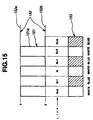
- Fig. 15 is a diagram (theory diagram for method 2) which represents the voltages (potentials) on the pixel electrodes 64 in the drum 91 and the common electrode 923 in the drum 92, together with a display pattern corresponding thereto.
- Method 2 i.e. the action of the electronic paper printer 1 is now described with reference to Fig. 15.
- the voltage 152 on the common electrode 923 is fluctuated between the maximum value of the voltage 151 on the pixel electrodes 64 (V volts in Fig. 15) and the minimum value thereof (0 volts in Fig. 15) (common potential oscillation). That is, when a one-row description is to be made in a desired row on the electronic paper 2, during the time that the gates of the thin film transistors 65 in the row corresponding to that row are turned on, the voltage 152 on the common electrode 923 is switched, either from V volts to 0 volts, or from 0 volts to V volts (setting to V volts and 0 volts on a time-division basis).
- the turning drive for the drums 91 and 92 is made a step drive, that is, description is performed while turning the drums 91 and 92 in steps.
- the display pattern 153 diagrammed in Fig. 15, for example, is to be described in a specific row on the electronic paper 2, and the gates of the thin film transistors 65 in the row corresponding to that row are turned on, the voltages indicated by the voltage pattern 151a are applied to the sources of those thin film transistors 65, that is, voltages of either 0 or V volts are applied.
- the voltage 152 on the common electrode 923 is held at the voltage indicated by the voltage pattern 152a, that is, to V volts, for a prescribed time, and then, when the gates of the thin film transistors 65 noted above continue to be turned on, [the voltage 152] is switched to the voltage indicated by the voltage pattern 152b, that is, to 0 volts, and held for a prescribed time.
- the voltage between the common electrode 923, on the one hand, and the pixel electrodes 64 in the (N-1) column, (N+1) column, and (N+3) column, on the other, is 0 volts, and no electric field is formed between these electrodes, wherefore the color of the display surface 20 of the electronic paper 2 is not changed in these portions, but is kept blue.
- the direction of the electric fields formed between the pixel electrodes 64 and the common electrode 923 is determined by the voltages 151 on the pixel electrodes 64, and the display pattern 153 can be described in a prescribed row on the electronic paper 2.
- the colors in prescribed locations (pixels) on the display surface 20 of the electronic paper 2 are determined solely by the voltages 151 on the pixel electrodes 64, on a one-to-one basis. Therefore, irrespective of what color the display surface 20 of the electronic paper 2 was before (prior to description), display patterns can be described on that electronic paper 2 merely with a single passage of the electronic paper 2 between the drum 91 and the drum 92 in the describing head 9 (i.e. a white and blue pattern is determined on a one-to-one basis). In other words, display patterns on the electronic paper 2 can be overwritten.
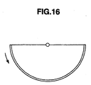
- the shape of the drums is cylindrical, but the drum shape is not limited thereto in the present invention, but may, for example, be shaped as a half drum as diagrammed in Fig. 16.
- the portion or portions of the head that come into contact with the electronic paper be shaped as a curved surface (i.e. that the electrode or electrodes be shaped as curved surfaces).
- the portions of the heads that contact the electronic paper are shaped as curved surfaces (with the shape of the drums in the heads being cylindrical or half-drums, for example), wherefore display patterns can be described properly and definitely on the electronic paper.
Landscapes
- Electrochromic Elements, Electrophoresis, Or Variable Reflection Or Absorption Elements (AREA)
- Devices For Indicating Variable Information By Combining Individual Elements (AREA)
- Printers Or Recording Devices Using Electromagnetic And Radiation Means (AREA)
Applications Claiming Priority (2)
| Application Number | Priority Date | Filing Date | Title |
|---|---|---|---|
| JP30151298 | 1998-10-22 | ||
| JP30151298A JP4138106B2 (ja) | 1998-10-22 | 1998-10-22 | 電子ペーパー用プリンター |
Publications (3)
| Publication Number | Publication Date |
|---|---|
| EP1000741A2 true EP1000741A2 (de) | 2000-05-17 |
| EP1000741A3 EP1000741A3 (de) | 2000-08-09 |
| EP1000741B1 EP1000741B1 (de) | 2009-04-01 |
Family
ID=17897827
Family Applications (1)
| Application Number | Title | Priority Date | Filing Date |
|---|---|---|---|
| EP99120725A Expired - Lifetime EP1000741B1 (de) | 1998-10-22 | 1999-10-19 | Drucker für elektronisches Papier |
Country Status (7)
| Country | Link |
|---|---|
| US (3) | US20020141801A1 (de) |
| EP (1) | EP1000741B1 (de) |
| JP (1) | JP4138106B2 (de) |
| KR (2) | KR100584784B1 (de) |
| CN (1) | CN1154567C (de) |
| DE (1) | DE69940660D1 (de) |
| TW (1) | TW436427B (de) |
Cited By (10)
| Publication number | Priority date | Publication date | Assignee | Title |
|---|---|---|---|---|
| WO2001091096A1 (en) * | 2000-05-26 | 2001-11-29 | Seiko Epson Corporation | Display and recorded medium |
| DE10117906A1 (de) * | 2001-04-10 | 2002-10-24 | Hubert Schmucker | Mobiles Datensichthandgerät |
| EP1184714A3 (de) * | 2000-08-31 | 2003-09-17 | Seiko Epson Corporation | Elektrophoretische Anzeigevorrichtung |
| WO2003034137A3 (en) * | 2001-10-16 | 2003-11-27 | Hewlett Packard Co | Portable electronic reading apparatus |
| US6738050B2 (en) | 1998-05-12 | 2004-05-18 | E Ink Corporation | Microencapsulated electrophoretic electrostatically addressed media for drawing device applications |
| US6816147B2 (en) | 2000-08-17 | 2004-11-09 | E Ink Corporation | Bistable electro-optic display, and method for addressing same |
| US6864875B2 (en) | 1998-04-10 | 2005-03-08 | E Ink Corporation | Full color reflective display with multichromatic sub-pixels |
| US7167155B1 (en) | 1995-07-20 | 2007-01-23 | E Ink Corporation | Color electrophoretic displays |
| EP1598709A3 (de) * | 2004-05-19 | 2007-03-28 | Samsung Electronics Co., Ltd. | Medium zur Erzeugung latenter Elektrostatischer Bilder mittels einer TFT matrix und Bilderzeugungsvorrichtung mit diesem Medium |
| US11747699B1 (en) * | 2022-07-19 | 2023-09-05 | Wistron Corporation | Electronic paper carrier and image update machine |
Families Citing this family (48)
| Publication number | Priority date | Publication date | Assignee | Title |
|---|---|---|---|---|
| US6704133B2 (en) | 1998-03-18 | 2004-03-09 | E-Ink Corporation | Electro-optic display overlays and systems for addressing such displays |
| JP4138106B2 (ja) * | 1998-10-22 | 2008-08-20 | セイコーエプソン株式会社 | 電子ペーパー用プリンター |
| JP2001350365A (ja) * | 2000-06-05 | 2001-12-21 | Minolta Co Ltd | 画像形成装置 |
| JP3750565B2 (ja) * | 2000-06-22 | 2006-03-01 | セイコーエプソン株式会社 | 電気泳動表示装置の駆動方法、駆動回路、および電子機器 |
| JP3925080B2 (ja) * | 2000-12-01 | 2007-06-06 | セイコーエプソン株式会社 | 電子ブック、それに用いる電子ペーパの製造方法 |
| US20030137496A1 (en) * | 2002-01-23 | 2003-07-24 | Chad Stevens | Systems and methods for facilitating interaction with a whiteboard |
| US8681352B2 (en) * | 2002-04-18 | 2014-03-25 | Hewlett-Packard Development Company, L.P. | Pull based computer output devices |
| US7584888B2 (en) * | 2002-06-04 | 2009-09-08 | Industrial Technology Research Institute | Item tag with liquid crystal display and image |
| US7161590B2 (en) * | 2002-09-04 | 2007-01-09 | John James Daniels | Thin, lightweight, flexible, bright, wireless display |
| KR100503413B1 (ko) * | 2002-10-31 | 2005-07-22 | 한국전자통신연구원 | 탬플릿 형태의 전기영동 디스플레이 및 그 제조방법 |
| CN1286655C (zh) | 2003-02-21 | 2006-11-29 | 精工爱普生株式会社 | 彩色电子纸写入装置及写入方法 |
| US20050263903A1 (en) * | 2003-08-30 | 2005-12-01 | Visible Tech-Knowledgy, Inc. | Method for pattern metalization of substrates |
| US20060017659A1 (en) * | 2004-04-28 | 2006-01-26 | Matsushita Electric Industrial Co., Ltd. | Electronic paper display system |
| KR100700523B1 (ko) * | 2005-02-11 | 2007-03-29 | 엘지전자 주식회사 | 충돌 대전형 전자종이 표시소자 및 그 제조 방법 |
| US7812813B2 (en) * | 2006-10-12 | 2010-10-12 | International Business Machines Corporation | ePaper stamp |
| KR101481821B1 (ko) * | 2007-08-24 | 2015-01-12 | 삼성전자주식회사 | 전자 종이에 이미지를 기록하기 위한 장치 |
| JP5184970B2 (ja) * | 2008-05-28 | 2013-04-17 | トッパン・フォームズ株式会社 | 表示制御装置 |
| US8457013B2 (en) | 2009-01-13 | 2013-06-04 | Metrologic Instruments, Inc. | Wireless dual-function network device dynamically switching and reconfiguring from a wireless network router state of operation into a wireless network coordinator state of operation in a wireless communication network |
| US8234507B2 (en) | 2009-01-13 | 2012-07-31 | Metrologic Instruments, Inc. | Electronic-ink display device employing a power switching mechanism automatically responsive to predefined states of device configuration |
| JP5540851B2 (ja) | 2009-06-04 | 2014-07-02 | セイコーエプソン株式会社 | 表示装置および表示シート |
| TW201109769A (en) * | 2009-09-02 | 2011-03-16 | Ind Tech Res Inst | Multistable display system and method for writing image on multistable display |
| US20110065081A1 (en) * | 2009-09-17 | 2011-03-17 | Shengmin Wen | Electrically erasable writable educational flash card |
| JP5402653B2 (ja) * | 2010-01-13 | 2014-01-29 | 富士ゼロックス株式会社 | 像保持体及びこれを用いた画像形成装置 |
| JP2011170189A (ja) * | 2010-02-19 | 2011-09-01 | Seiko Epson Corp | 電子ペーパーへの画像記録装置及び画像記録方法 |
| JP2011170045A (ja) * | 2010-02-17 | 2011-09-01 | Seiko Epson Corp | 電子ペーパーへの画像記録装置及び画像記録方法 |
| JP2011164145A (ja) * | 2010-02-04 | 2011-08-25 | Seiko Epson Corp | 電子ペーパーへの画像記録装置及び画像記録方法 |
| KR101114762B1 (ko) * | 2010-02-05 | 2012-02-29 | 삼성전자주식회사 | 컬러 전자 종이 키패드 장치 |
| TWI431565B (zh) * | 2010-05-20 | 2014-03-21 | Prime View Int Co Ltd | 電子紙刷寫裝置及方法 |
| US20110298760A1 (en) | 2010-06-02 | 2011-12-08 | Omer Gila | Systems and methods for writing on and using electronic paper |
| CN102289124A (zh) * | 2010-06-18 | 2011-12-21 | 元太科技工业股份有限公司 | 电子纸刷写装置及方法 |
| CN102314037A (zh) * | 2010-07-06 | 2012-01-11 | 群康科技(深圳)有限公司 | 显示组件、显示装置与显示组件的制造方法 |
| TWI463450B (zh) * | 2010-07-28 | 2014-12-01 | E Ink Holdings Inc | 顯示器及其製造方法 |
| US8587622B2 (en) * | 2011-02-25 | 2013-11-19 | Xerox Corporation | Generation of digital electrostatic latent images and data communications system using rotary contacts |
| KR101260013B1 (ko) * | 2011-04-29 | 2013-05-06 | 인텔렉추얼디스커버리 주식회사 | 전자 종이용 데이터 기록 장치 및 이를 이용한 데이터 기록 방법 |
| KR101275338B1 (ko) * | 2012-10-15 | 2013-06-17 | 삼성전기주식회사 | 전자종이 표시장치 |
| CN102929065B (zh) * | 2012-10-19 | 2016-05-25 | 京东方科技集团股份有限公司 | 一种电子纸打印装置以及打印方法 |
| US8941636B2 (en) | 2013-01-31 | 2015-01-27 | Hewlett-Packard Development Company, L.P. | E-paper printing system |
| CN103092038B (zh) * | 2013-02-20 | 2016-05-04 | 吴涛 | 一种打印、复印方法和设备 |
| EP3100111B1 (de) | 2014-01-31 | 2020-01-22 | Hewlett-Packard Development Company, L.P. | Anzeigevorrichtung |
| WO2016133224A1 (ja) * | 2015-02-18 | 2016-08-25 | 株式会社オルガノサーキット | ドラム型電子ペーパーライター |
| US10126626B1 (en) | 2015-03-23 | 2018-11-13 | Amazon Technologies, Inc. | Reusable electrically printable medium |
| US9304449B1 (en) * | 2015-03-23 | 2016-04-05 | Amazon Technologies, Inc. | Printer for reusable electrically printable medium |
| WO2017074340A1 (en) | 2015-10-28 | 2017-05-04 | Hewlett-Packard Development Company, L.P. | Passive e-paper imaging |
| WO2017074396A1 (en) * | 2015-10-29 | 2017-05-04 | Hewlett-Packard Development Company, L.P. | E-paper imager |
| JP2016026328A (ja) * | 2015-10-30 | 2016-02-12 | 株式会社半導体エネルギー研究所 | 電気泳動表示装置 |
| CN108292070B (zh) * | 2015-10-30 | 2021-03-09 | 惠普发展公司,有限责任合伙企业 | 用于可重写显示介质的带驱动器 |
| US12180746B2 (en) * | 2021-05-17 | 2024-12-31 | Knoll, Inc. | Storage apparatus |
| KR20230091729A (ko) | 2021-12-16 | 2023-06-23 | 이윤형 | 열인화 종이 말림 방지 장치 및 이를 구비한 열인화 종이 프린터 |
Family Cites Families (27)
| Publication number | Priority date | Publication date | Assignee | Title |
|---|---|---|---|---|
| US2283752A (en) * | 1940-05-10 | 1942-05-19 | Faust R Gonsett | Eye shield |
| JPS5244197A (en) | 1975-10-03 | 1977-04-06 | Hitachi Ltd | Display panel |
| JPS5468238A (en) | 1977-11-10 | 1979-06-01 | Nec Corp | Electrode for electrostatic recording |
| JPS61115649A (ja) | 1984-11-07 | 1986-06-03 | Sumitomo Metal Ind Ltd | スラブの連続鋳造方法 |
| JPS6238626A (ja) | 1985-08-13 | 1987-02-19 | Toa Tokushu Denki Kk | サ−ビス・エリア・チエツク装置 |
| JPS62149024A (ja) | 1985-12-23 | 1987-07-03 | Fuji Electric Co Ltd | 磁気記録媒体 |
| NL8601376A (nl) * | 1986-05-29 | 1987-12-16 | Oce Nederland Bv | Beeldvormingselement voor een elektrostatische drukinrichting, alsmede een drukinrichting waarin zulk een element wordt toegepast. |
| JPH0748786B2 (ja) * | 1989-10-04 | 1995-05-24 | 富士ゼロックス株式会社 | イメージセンサ |
| CA2027440C (en) | 1989-11-08 | 1995-07-04 | Nicholas K. Sheridon | Paper-like computer output display and scanning system therefor |
| JP3282220B2 (ja) | 1992-07-15 | 2002-05-13 | 富士ゼロックス株式会社 | 電気泳動型画像複写装置およびその複写画像を保持するための電気泳動型画像表示シート |
| JP3233463B2 (ja) * | 1992-09-25 | 2001-11-26 | 株式会社東芝 | 像形成体、この像形成体を含む像担持体及びこの像形成体を組み込んだ画像形成装置並びに画像形成方法 |
| US5604027A (en) * | 1995-01-03 | 1997-02-18 | Xerox Corporation | Some uses of microencapsulation for electric paper |
| JPH0916116A (ja) | 1995-06-26 | 1997-01-17 | Nok Corp | 電気泳動表示装置 |
| US5723204A (en) * | 1995-12-26 | 1998-03-03 | Xerox Corporation | Two-sided electrical paper |
| US5961804A (en) * | 1997-03-18 | 1999-10-05 | Massachusetts Institute Of Technology | Microencapsulated electrophoretic display |
| US6980196B1 (en) | 1997-03-18 | 2005-12-27 | Massachusetts Institute Of Technology | Printable electronic display |
| US5866284A (en) * | 1997-05-28 | 1999-02-02 | Hewlett-Packard Company | Print method and apparatus for re-writable medium |
| US6100909A (en) * | 1998-03-02 | 2000-08-08 | Xerox Corporation | Matrix addressable array for digital xerography |
| US6064410A (en) * | 1998-03-03 | 2000-05-16 | Eastman Kodak Company | Printing continuous tone images on receivers having field-driven particles |
| EP0940261A1 (de) * | 1998-03-05 | 1999-09-08 | Eastman Kodak Company | Herstellung von Bildern auf Empfänger die feldgesteuerte Teilchen enthalten |
| US6177947B1 (en) * | 1998-04-02 | 2001-01-23 | Eastman Kodak Company | Color image formation in receivers having field-driven particles |
| JP4651193B2 (ja) * | 1998-05-12 | 2011-03-16 | イー インク コーポレイション | ドローイングデバイス用途のためのマイクロカプセル化した電気泳動性の静電的にアドレスした媒体 |
| JP4061734B2 (ja) * | 1998-09-30 | 2008-03-19 | ブラザー工業株式会社 | 表示媒体の表示方法及び表示装置 |
| JP4138106B2 (ja) * | 1998-10-22 | 2008-08-20 | セイコーエプソン株式会社 | 電子ペーパー用プリンター |
| US6531997B1 (en) * | 1999-04-30 | 2003-03-11 | E Ink Corporation | Methods for addressing electrophoretic displays |
| US6795101B2 (en) * | 2001-04-27 | 2004-09-21 | Oce-Technologies B.V. | Direct imaging process with feed back control by measuring the amount of toner deposited |
| JP2006235013A (ja) * | 2005-02-23 | 2006-09-07 | Seiko Epson Corp | 電気泳動装置、及び電子機器 |
-
1998
- 1998-10-22 JP JP30151298A patent/JP4138106B2/ja not_active Expired - Fee Related
-
1999
- 1999-10-19 DE DE69940660T patent/DE69940660D1/de not_active Expired - Lifetime
- 1999-10-19 EP EP99120725A patent/EP1000741B1/de not_active Expired - Lifetime
- 1999-10-21 CN CNB99121871XA patent/CN1154567C/zh not_active Expired - Fee Related
- 1999-10-21 TW TW088118363A patent/TW436427B/zh not_active IP Right Cessation
- 1999-10-21 US US09/422,378 patent/US20020141801A1/en not_active Abandoned
- 1999-10-22 KR KR1019990046117A patent/KR100584784B1/ko not_active Expired - Fee Related
-
2004
- 2004-07-14 US US10/891,254 patent/US7114864B2/en not_active Expired - Fee Related
-
2005
- 2005-12-30 KR KR1020050135704A patent/KR100635965B1/ko not_active Expired - Fee Related
-
2006
- 2006-04-26 US US11/412,226 patent/US7381000B2/en not_active Expired - Fee Related
Non-Patent Citations (1)
| Title |
|---|
| BARRETT COMISKEY; JONATHAN D. ALBERT; JOE JACOBSON: "Electrophoretic Ink: A printable display material", PROCEEDINGS OF SID 97 IN BOSTON, 1997 |
Cited By (18)
| Publication number | Priority date | Publication date | Assignee | Title |
|---|---|---|---|---|
| US7167155B1 (en) | 1995-07-20 | 2007-01-23 | E Ink Corporation | Color electrophoretic displays |
| US6864875B2 (en) | 1998-04-10 | 2005-03-08 | E Ink Corporation | Full color reflective display with multichromatic sub-pixels |
| US7075502B1 (en) | 1998-04-10 | 2006-07-11 | E Ink Corporation | Full color reflective display with multichromatic sub-pixels |
| US8466852B2 (en) | 1998-04-10 | 2013-06-18 | E Ink Corporation | Full color reflective display with multichromatic sub-pixels |
| US6738050B2 (en) | 1998-05-12 | 2004-05-18 | E Ink Corporation | Microencapsulated electrophoretic electrostatically addressed media for drawing device applications |
| US6842165B2 (en) | 2000-05-26 | 2005-01-11 | Seiko Epson Corporation | Display device and recording medium |
| WO2001091096A1 (en) * | 2000-05-26 | 2001-11-29 | Seiko Epson Corporation | Display and recorded medium |
| US6816147B2 (en) | 2000-08-17 | 2004-11-09 | E Ink Corporation | Bistable electro-optic display, and method for addressing same |
| US7280094B2 (en) | 2000-08-17 | 2007-10-09 | E Ink Corporation | Bistable electro-optic display, and method for addressing same |
| US6987503B2 (en) | 2000-08-31 | 2006-01-17 | Seiko Epson Corporation | Electrophoretic display |
| EP1184714A3 (de) * | 2000-08-31 | 2003-09-17 | Seiko Epson Corporation | Elektrophoretische Anzeigevorrichtung |
| DE10117906A1 (de) * | 2001-04-10 | 2002-10-24 | Hubert Schmucker | Mobiles Datensichthandgerät |
| DE10117906B4 (de) * | 2001-04-10 | 2004-11-18 | Hubert Schmucker | Handgerät zur Anzeige von Daten |
| US6940497B2 (en) | 2001-10-16 | 2005-09-06 | Hewlett-Packard Development Company, L.P. | Portable electronic reading apparatus |
| WO2003034137A3 (en) * | 2001-10-16 | 2003-11-27 | Hewlett Packard Co | Portable electronic reading apparatus |
| EP1598709A3 (de) * | 2004-05-19 | 2007-03-28 | Samsung Electronics Co., Ltd. | Medium zur Erzeugung latenter Elektrostatischer Bilder mittels einer TFT matrix und Bilderzeugungsvorrichtung mit diesem Medium |
| US7388594B2 (en) | 2004-05-19 | 2008-06-17 | Samsung Electronics Co., Ltd. | Electrostatic latent image forming medium, image forming apparatus including the electrostatic latent image forming medium and method of forming an electrostatic latent image |
| US11747699B1 (en) * | 2022-07-19 | 2023-09-05 | Wistron Corporation | Electronic paper carrier and image update machine |
Also Published As
| Publication number | Publication date |
|---|---|
| JP2000127478A (ja) | 2000-05-09 |
| EP1000741B1 (de) | 2009-04-01 |
| JP4138106B2 (ja) | 2008-08-20 |
| TW436427B (en) | 2001-05-28 |
| US20060210339A1 (en) | 2006-09-21 |
| US7114864B2 (en) | 2006-10-03 |
| KR20000029263A (ko) | 2000-05-25 |
| KR100635965B1 (ko) | 2006-10-18 |
| US7381000B2 (en) | 2008-06-03 |
| KR20060012559A (ko) | 2006-02-08 |
| US20040247360A1 (en) | 2004-12-09 |
| DE69940660D1 (de) | 2009-05-14 |
| EP1000741A3 (de) | 2000-08-09 |
| CN1154567C (zh) | 2004-06-23 |
| US20020141801A1 (en) | 2002-10-03 |
| CN1252538A (zh) | 2000-05-10 |
| KR100584784B1 (ko) | 2006-05-30 |
Similar Documents
| Publication | Publication Date | Title |
|---|---|---|
| US7381000B2 (en) | Electronic paper printer | |
| US6879430B2 (en) | Image display medium and image writing device | |
| US7292231B2 (en) | Writing device for color electronic paper | |
| US6842165B2 (en) | Display device and recording medium | |
| US7106297B2 (en) | Color display device | |
| US8928575B2 (en) | Electrophoretic display device, electronic apparatus, and method of driving electrophoretic display device | |
| CN101840669A (zh) | 电泳显示设备及其驱动方法 | |
| US8350802B2 (en) | Electrophoretic device with capacitive storage and applied fluctuating signal, method of driving the same, and electronic apparatus | |
| JP3956493B2 (ja) | 電気泳動表示装置 | |
| US20090223821A1 (en) | Electrophoretic device, method for driving same, and electronic apparatus | |
| US20090096773A1 (en) | Electrophoretic display device, electronic apparatus, and method of driving electrophoretic display device | |
| JPS5939794B2 (ja) | 電位記録プリント装置 | |
| US20050104845A1 (en) | Driving apparatus of electronic ink display device and method therefor | |
| KR100565196B1 (ko) | 전자잉크 표시 패널 구동 장치 및 방법 | |
| JP4389458B2 (ja) | カラー電子ペーパ書込み装置及びカラー電子ペーパ書込み方法 | |
| JPH11212501A (ja) | 画像形成装置 | |
| JP5517426B2 (ja) | 表示装置 | |
| JPH01298375A (ja) | 多色画像表示装置 | |
| KR20050047343A (ko) | 전자잉크 표시 패널 구동 방법 | |
| JP2022157571A (ja) | 表示装置の駆動方法 | |
| JP2004252308A (ja) | カラー表示媒体の書込み装置 | |
| JP2009244487A (ja) | 表示パネル、その帯電粒子供給方法 |
Legal Events
| Date | Code | Title | Description |
|---|---|---|---|
| PUAI | Public reference made under article 153(3) epc to a published international application that has entered the european phase |
Free format text: ORIGINAL CODE: 0009012 |
|
| AK | Designated contracting states |
Kind code of ref document: A2 Designated state(s): DE FR GB NL |
|
| AX | Request for extension of the european patent |
Free format text: AL;LT;LV;MK;RO;SI |
|
| PUAL | Search report despatched |
Free format text: ORIGINAL CODE: 0009013 |
|
| AK | Designated contracting states |
Kind code of ref document: A3 Designated state(s): AT BE CH CY DE DK ES FI FR GB GR IE IT LI LU MC NL PT SE |
|
| AX | Request for extension of the european patent |
Free format text: AL;LT;LV;MK;RO;SI |
|
| 17P | Request for examination filed |
Effective date: 20010117 |
|
| AKX | Designation fees paid |
Free format text: DE FR GB NL |
|
| 17Q | First examination report despatched |
Effective date: 20060901 |
|
| GRAP | Despatch of communication of intention to grant a patent |
Free format text: ORIGINAL CODE: EPIDOSNIGR1 |
|
| GRAP | Despatch of communication of intention to grant a patent |
Free format text: ORIGINAL CODE: EPIDOSNIGR1 |
|
| GRAS | Grant fee paid |
Free format text: ORIGINAL CODE: EPIDOSNIGR3 |
|
| GRAA | (expected) grant |
Free format text: ORIGINAL CODE: 0009210 |
|
| AK | Designated contracting states |
Kind code of ref document: B1 Designated state(s): DE FR GB NL |
|
| REG | Reference to a national code |
Ref country code: GB Ref legal event code: FG4D |
|
| REF | Corresponds to: |
Ref document number: 69940660 Country of ref document: DE Date of ref document: 20090514 Kind code of ref document: P |
|
| NLV1 | Nl: lapsed or annulled due to failure to fulfill the requirements of art. 29p and 29m of the patents act | ||
| PG25 | Lapsed in a contracting state [announced via postgrant information from national office to epo] |
Ref country code: NL Free format text: LAPSE BECAUSE OF FAILURE TO SUBMIT A TRANSLATION OF THE DESCRIPTION OR TO PAY THE FEE WITHIN THE PRESCRIBED TIME-LIMIT Effective date: 20090401 |
|
| PLBE | No opposition filed within time limit |
Free format text: ORIGINAL CODE: 0009261 |
|
| STAA | Information on the status of an ep patent application or granted ep patent |
Free format text: STATUS: NO OPPOSITION FILED WITHIN TIME LIMIT |
|
| 26N | No opposition filed |
Effective date: 20100105 |
|
| PGFP | Annual fee paid to national office [announced via postgrant information from national office to epo] |
Ref country code: FR Payment date: 20141008 Year of fee payment: 16 Ref country code: DE Payment date: 20141014 Year of fee payment: 16 Ref country code: GB Payment date: 20141015 Year of fee payment: 16 |
|
| REG | Reference to a national code |
Ref country code: DE Ref legal event code: R119 Ref document number: 69940660 Country of ref document: DE |
|
| GBPC | Gb: european patent ceased through non-payment of renewal fee |
Effective date: 20151019 |
|
| PG25 | Lapsed in a contracting state [announced via postgrant information from national office to epo] |
Ref country code: GB Free format text: LAPSE BECAUSE OF NON-PAYMENT OF DUE FEES Effective date: 20151019 Ref country code: DE Free format text: LAPSE BECAUSE OF NON-PAYMENT OF DUE FEES Effective date: 20160503 |
|
| REG | Reference to a national code |
Ref country code: FR Ref legal event code: ST Effective date: 20160630 |
|
| PG25 | Lapsed in a contracting state [announced via postgrant information from national office to epo] |
Ref country code: FR Free format text: LAPSE BECAUSE OF NON-PAYMENT OF DUE FEES Effective date: 20151102 |