EP1001335A1 - Datenverarbeitungseinheit mit einer Koprozessorschnittstelle - Google Patents
Datenverarbeitungseinheit mit einer Koprozessorschnittstelle Download PDFInfo
- Publication number
- EP1001335A1 EP1001335A1 EP99116655A EP99116655A EP1001335A1 EP 1001335 A1 EP1001335 A1 EP 1001335A1 EP 99116655 A EP99116655 A EP 99116655A EP 99116655 A EP99116655 A EP 99116655A EP 1001335 A1 EP1001335 A1 EP 1001335A1
- Authority
- EP
- European Patent Office
- Prior art keywords
- coprocessor
- instruction
- data processing
- processing unit
- execution
- Prior art date
- Legal status (The legal status is an assumption and is not a legal conclusion. Google has not performed a legal analysis and makes no representation as to the accuracy of the status listed.)
- Granted
Links
Images


Classifications
-
- G—PHYSICS
- G06—COMPUTING OR CALCULATING; COUNTING
- G06F—ELECTRIC DIGITAL DATA PROCESSING
- G06F9/00—Arrangements for program control, e.g. control units
- G06F9/06—Arrangements for program control, e.g. control units using stored programs, i.e. using an internal store of processing equipment to receive or retain programs
- G06F9/30—Arrangements for executing machine instructions, e.g. instruction decode
- G06F9/38—Concurrent instruction execution, e.g. pipeline or look ahead
- G06F9/3885—Concurrent instruction execution, e.g. pipeline or look ahead using a plurality of independent parallel functional units
- G06F9/3893—Concurrent instruction execution, e.g. pipeline or look ahead using a plurality of independent parallel functional units controlled in tandem, e.g. multiplier-accumulator
- G06F9/3895—Concurrent instruction execution, e.g. pipeline or look ahead using a plurality of independent parallel functional units controlled in tandem, e.g. multiplier-accumulator for complex operations, e.g. multidimensional or interleaved address generators, macros
- G06F9/3897—Concurrent instruction execution, e.g. pipeline or look ahead using a plurality of independent parallel functional units controlled in tandem, e.g. multiplier-accumulator for complex operations, e.g. multidimensional or interleaved address generators, macros with adaptable data path
-
- G—PHYSICS
- G06—COMPUTING OR CALCULATING; COUNTING
- G06F—ELECTRIC DIGITAL DATA PROCESSING
- G06F9/00—Arrangements for program control, e.g. control units
- G06F9/06—Arrangements for program control, e.g. control units using stored programs, i.e. using an internal store of processing equipment to receive or retain programs
- G06F9/30—Arrangements for executing machine instructions, e.g. instruction decode
- G06F9/38—Concurrent instruction execution, e.g. pipeline or look ahead
- G06F9/3877—Concurrent instruction execution, e.g. pipeline or look ahead using a secondary processor, e.g. coprocessor
-
- G—PHYSICS
- G06—COMPUTING OR CALCULATING; COUNTING
- G06F—ELECTRIC DIGITAL DATA PROCESSING
- G06F9/00—Arrangements for program control, e.g. control units
- G06F9/06—Arrangements for program control, e.g. control units using stored programs, i.e. using an internal store of processing equipment to receive or retain programs
- G06F9/30—Arrangements for executing machine instructions, e.g. instruction decode
- G06F9/38—Concurrent instruction execution, e.g. pipeline or look ahead
- G06F9/3885—Concurrent instruction execution, e.g. pipeline or look ahead using a plurality of independent parallel functional units
Definitions
- the present invention relates to a data processing unit with a coprocessor interface.
- a coprocessor is used in a data processing system to perform special tasks, such as floating point operations, digital signal processing, etc.
- Many data processors are capable of working in combination with a coprocessor.
- a main processor addresses a coprocessor through the system bus. If the main processor decodes a coprocessor instruction, it transfers, for example by means of an exception routine, the coprocessor instruction and respective data to a coprocessor which performs the instruction and transfers back a result to the main processor.
- the main processor usually is set in a wait state.
- U.S. patent 5,603,047 describes such a system.
- Fig. 7 of 5,603,047 shows a block diagram of such a coprocessor having 24 registers.
- a coprocessor instruction has a specific format which is detected during the decode stage of the pipeline shown in Fig. 2 of 5,603,047.
- the respective coprocessor instructions are described in column 20 of the 5,603,047. They include instructions for loading and storing data and control from or to the coprocessor.
- the coprocessor can be able to perform a variety of functions which might be selected by various programs which can be selected through respective addresses which are transferred to the coprocessor.
- the coprocessor executes these programs and when finished, the respective results can be transferred to the main processor through respective transfer instructions.
- a data processing unit comprising a register file, a memory, a plurality of execution units, a pipeline configuration for processing instructions having a fetch stage for fetching an instruction from said memory, a decode stage for decoding an operational code from the instruction, an execution stage for activating one of the execution units, and a write-back stage for writing back from the execution unit, a coprocessor interface for coupling at least one coprocessor.
- the data processing unit has read- and write-lines coupling the register file with the coprocessor for exchanging operands, at least one control line indicating that the coprocessor is busy, a plurality of control lines from the decode stage for controlling said coprocessor which are operated upon detection of a coprocessor instruction.
- the coprocessor is using the registers from the register file during execution of a coprocessor instruction.
- the coprocessor is using the register file of the main processor it can execute instructions as fast as any execution unit, such as the arithmetic logic unit, a shifter, a load/store unit, etc.
- a coprocessor instruction is decoded and executed in the same manner as any other instruction.
- a field programmable gate array (FPGA) is used as a coprocessor.
- FPGA field programmable gate array
- Fig.1 shows a memory cache subsystem 1 coupled through a bus with a register file 2.
- Register file 2 contains an align unit 201, address buffer 202 and data buffer 207, address registers 203 and data registers 208, address forwarding unit 204 and data forwarding unit 209, address write-back buffer 205 and data write-back buffer 210, and a control unit 206.
- the data registers are interfaced with the coprocessor. Therefore, only the most relevant connecting lines are shown in Fig.1 for the sake of a better overview. Nevertheless any kind of register from a register file can be used to interface with the coprocessor interface.
- the data registers 208 are coupled through data buffer 207 and align unit 201 with the cache memory subsystem 1.
- the first read bus 211 comprises 64 bit lines
- the second read bus 212 has 32 bit lines
- the third read bus 213 provides also 32 bit lines.
- the number of bit lines per read port is freely selectable and depends on the instruction set.
- a write bus 214 having 64 bit lines is provided. These four busses 211, 212, 213, and 214 allow read and write access to the respective data registers 208 of the register file 2.
- An instruction fetch unit 5 provides instructions to a following instruction decoder 6.
- the instruction decoder 6 provides all execution units with respective operational codes and selects the respective registers 203, 208 in the register file 2.
- a coprocessor interface 7 is provided which is coupled with the four busses 211, 212, 213, and 214. Furthermore, coprocessor interface 7 is coupled through busses 61 and 62 with instruction decoder 6. Bus 61 can have n instruction lines for providing operational code and other information. In addition, bus 62 has m control lines to provide the pipeline with status information from the coprocessors.
- the control bus 61, 62 can have the following functionality: One line can indicate a valid instruction which would be asserted when the integer pipeline is valid. Another line or set of lines could be provided for an instruction sequencer. Depending on the number of instruction cycles needed a 2 bit , 3bit, 4 bit, etc., -wide bus would be provided. A further line can indicate a multi cycle start which would be activated by the coprocessor to indicate when the instruction in the coprocessor decoder is a multi cycle instruction. Yet another line would be activated by the coprocessor to indicate the end of a multi cycle instruction, signaling the last re-inject of the instruction.
- a multi cycle continue control line can be provided which would be activated by the coprocessor to re-inject an instruction during multi cycle start and end phase.
- a further control line may be provided.
- Further control lines indicate which coprocessor has to be enabled, for example, two lines can address four different coprocessors. Other control signals may be provided depending on the structure of the coprocessor unit.
- the embodiment according to Fig. 1 shows three coprocessors.
- the number of coprocessors which can be added to the system internally or externally depends on the instruction size of the data processing unit as will be explained later.
- the first coprocessor 4a in this embodiment shows a floating point coprocessor.
- the second coprocessor 4b is a fuzzy logic coprocessor and the third coprocessor is a re-programmable coprocessor in form of a FPGA. All coprocessors are coupled with the six busses 211,212,213,214, 61, and 62 through interface 7.
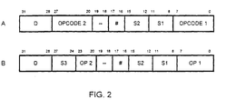
- Fig. 2 shows two possible formats A and B of a coprocessor instruction.
- an instruction is 32 bits long and the bit fields indicating a coprocessor instruction can be one or both of the opcode fields OPCODE 1, OPCODE 2, and OP 1, OP2, respectively.
- the bit field D indicates the destination in form of a register number where the result of the respective instruction will be written to.
- the bit field # indicates the number of the coprocessor for executing the instruction defined in the opcode bit field.
- Bit fields S1, S2, S3 contain either data register or immediate data for the respective instruction. In this embodiment each of the bit field S1, S2, S3, and D are 4 bits wide, the OPCODE field comprises 12 or 16 bits.
- the # field has 2 bits, and the 2 bits are not used in both instruction formats A and B indicated as "--".
- Instruction fetch unit 5 provides instruction decoder 6 with an instruction from a instruction stream. Instruction decoder 6 determines whether an instruction is designated to a coprocessor by means of the bit field OPCODE 1, OPCODE 2, and OP 1, OP 2, respectively. After decoding of an instruction the coprocessor indicated in the bit field # receives the respective instruction stored in the opcode bit fields and eventually immediate data from one or more of the bit fields S1, S2, S3 through bus 61 and the contents of the selected data registers in bit fields S1, S2, and S3 through the three data read busses 211, 212, and 213.
- the coprocessor executes the instruction decoded by the instruction decoder and writes during the write-back cycle the respective result back to a data register designated in bit field D.
- execution of a coprocessor instruction can be as quick as an execution of any execution units. No transfers from or to registers are delaying the process of executing a special instruction because the respective coprocessor does not need its own registers. Nevertheless, a coprocessor may have additional registers which contain data that need not be accessible by the data processing unit.
- a common known coprocessor needs to be initialized by transferring data to the coprocessor, configuring the coprocessor and transferring the respective instruction to the coprocessor. This creates an overhead affecting the overall speed of the system.
- a known coprocessor will stall the respective pipelines for a plurality of cycles.
- the coprocessor according to the present invention does not need these steps. It can operate directly with the register file of the main CPU. Transfer of data is similar to the transfer of data to regular execution units. Thus every instruction which can be executed in a single cycle can be executed in parallel with another pipeline or multiple pipelines. In the embodiment of Fig. 1 this would be the load/store pipeline coupled with the address register file 203, and the units 202, 204, 205.
- control lines indicating a multi-cycle start, a multi-cycle end, and a multi-cycle continuation described above are used.
- a microcontroller system using a data processing unit according to the present invention is programmed initially.
- the FPGA may be re-programmed and adapted to each specific task of a complex program dynamically.
- an instruction for performing a convolution operation is not available in standard instruction sets of either a RISC or a CISC processor.
- Such an instruction forms, for example, a 32 bit long word out of two 16 bit words by alternatively concatenating the bits of each input word. For example, if the first input word contains only "1111...111" and the second input word contains only "0" the result would be a 32 bit word with alternating "0" and "1".
- the resulting word consists of bit 16 of the first word, followed by bit 16 of the second word, followed by bit 15 of the first word and so on.
- a FPGA can be easily programmed to couple a multiplexer or respective logic with the input and output lines to perform this task in a single cycle. Because such an instruction can be performed with the registers of the data processing unit no additional transfers are necessary.
- the embodiment of a coprocessor interface provides three data read busses 211, 212, and 213 and one write-back bus 214.
- digital signal processing functionality can be provided by the coprocessors. For example, a single instruction can perform a multiplication of two operands and an addition of the result with a third operand. The final result is written into a designated register. All three operands can be transferred during the decode cycle to the respective coprocessor and written back to the destination register during the write-back cycle.
- Fig. 3 shows the main blocks of a coprocessor 4 coupled with a coprocessor interface according to the invention.
- Each coprocessor may have a decode unit 41 which receives the respective coprocessor instruction from the CPU.
- Decode unit 41 decodes the instruction, for example, bits 16 to 23 according to an instruction as shown in Fig. 2.
- decode unit 41 provides an execute unit 42 coupled with decode unit 41 with the respective control signals.
- Execute unit may contain multiplexers, adders, shifter, etc. connected in a way to perform respective functions.
- the control signals provided by decode unit 41 activate the respective units to operate in a predetermined way.
- the result is passed to the coprocessor interface, which couples the result bus to the write back bus of the integer pipeline.
- the coprocessor behaves in a similar way as an additional execution unit as shown in Fig. 1.
- Fig. 4 shows a solution where multiple execution units 43, 44, 45, and 46 share the same decode unit 41.
- Decode unit 41 decodes the respective coprocessor instruction and selects one of the execution units 43, 44, 45, or 46 which performs the respective function. The result is again written back through interface 7 into the register file.
- additional control lines 62 are provided which supply information from the coprocessors to the pipeline as described above.
- the coprocessor executing a respective instruction which needs a plurality of system cycles sends a busy signal through bus 62 to the instruction decode unit 6 to stall the pipeline.
- the coprocessor interface includes all necessary buffers and logic to feed necessary signals from or to the coprocessors.
- the coprocessors according to the present invention can be coupled with the coprocessor interface 7 either on-chip or externally.
- the coprocessors are coupled with the integer pipeline.
- the coprocessor interface can also be coupled with a different type of pipeline or with more than one pipeline. Thus, two or more coprocessors could operate in parallel.
Landscapes
- Engineering & Computer Science (AREA)
- Software Systems (AREA)
- Theoretical Computer Science (AREA)
- Physics & Mathematics (AREA)
- General Engineering & Computer Science (AREA)
- General Physics & Mathematics (AREA)
- Advance Control (AREA)
Applications Claiming Priority (2)
| Application Number | Priority Date | Filing Date | Title |
|---|---|---|---|
| US189111 | 1994-01-31 | ||
| US09/189,111 US6434689B2 (en) | 1998-11-09 | 1998-11-09 | Data processing unit with interface for sharing registers by a processor and a coprocessor |
Publications (2)
| Publication Number | Publication Date |
|---|---|
| EP1001335A1 true EP1001335A1 (de) | 2000-05-17 |
| EP1001335B1 EP1001335B1 (de) | 2002-10-30 |
Family
ID=22695981
Family Applications (1)
| Application Number | Title | Priority Date | Filing Date |
|---|---|---|---|
| EP99116655A Expired - Lifetime EP1001335B1 (de) | 1998-11-09 | 1999-08-26 | Datenverarbeitungseinheit mit einer Koprozessorschnittstelle |
Country Status (3)
| Country | Link |
|---|---|
| US (1) | US6434689B2 (de) |
| EP (1) | EP1001335B1 (de) |
| DE (1) | DE69903704D1 (de) |
Cited By (3)
| Publication number | Priority date | Publication date | Assignee | Title |
|---|---|---|---|---|
| EP1422617A3 (de) * | 2002-11-19 | 2006-03-15 | STMicroelectronics, Inc. | Zusatzprozessorarchitektur auf Basis von einem Befehlsaufspaltungs-Transaktionsmodell |
| CN102750127A (zh) * | 2012-06-12 | 2012-10-24 | 清华大学 | 一种协处理器 |
| EP2525286A1 (de) | 2011-05-17 | 2012-11-21 | Nxp B.V. | Koprozessorschnittstelle |
Families Citing this family (33)
| Publication number | Priority date | Publication date | Assignee | Title |
|---|---|---|---|---|
| US6505290B1 (en) * | 1997-09-05 | 2003-01-07 | Motorola, Inc. | Method and apparatus for interfacing a processor to a coprocessor |
| JP2001092662A (ja) * | 1999-09-22 | 2001-04-06 | Toshiba Corp | プロセッサコア及びこれを用いたプロセッサ |
| JP2002041489A (ja) * | 2000-07-25 | 2002-02-08 | Mitsubishi Electric Corp | 同期信号生成回路、それを用いたプロセッサシステムおよび同期信号生成方法 |
| JP4125475B2 (ja) * | 2000-12-12 | 2008-07-30 | 株式会社東芝 | Rtl生成システム、rtl生成方法、rtl生成プログラム及び半導体装置の製造方法 |
| US7376811B2 (en) * | 2001-11-06 | 2008-05-20 | Netxen, Inc. | Method and apparatus for performing computations and operations on data using data steering |
| US6886092B1 (en) * | 2001-11-19 | 2005-04-26 | Xilinx, Inc. | Custom code processing in PGA by providing instructions from fixed logic processor portion to programmable dedicated processor portion |
| JP2006510129A (ja) * | 2002-12-12 | 2006-03-23 | コーニンクレッカ フィリップス エレクトロニクス エヌ ヴィ | システム・オン・チップへのアレイ・プロセッサのモジュラ統合 |
| US6996785B1 (en) | 2003-04-25 | 2006-02-07 | Universal Network Machines, Inc . | On-chip packet-based interconnections using repeaters/routers |
| US20050071830A1 (en) * | 2003-09-30 | 2005-03-31 | Starcore, Llc | Method and system for processing a sequence of instructions |
| US7441106B2 (en) * | 2004-07-02 | 2008-10-21 | Seagate Technology Llc | Distributed processing in a multiple processing unit environment |
| JP2006048661A (ja) * | 2004-07-06 | 2006-02-16 | Matsushita Electric Ind Co Ltd | プロセッサとコプロセッサとの間でのデータ転送を制御する演算処理装置 |
| US7395410B2 (en) * | 2004-07-06 | 2008-07-01 | Matsushita Electric Industrial Co., Ltd. | Processor system with an improved instruction decode control unit that controls data transfer between processor and coprocessor |
| US7546441B1 (en) * | 2004-08-06 | 2009-06-09 | Xilinx, Inc. | Coprocessor interface controller |
| US7346759B1 (en) | 2004-08-06 | 2008-03-18 | Xilinx, Inc. | Decoder interface |
| US7590823B1 (en) | 2004-08-06 | 2009-09-15 | Xilinx, Inc. | Method and system for handling an instruction not supported in a coprocessor formed using configurable logic |
| US7590822B1 (en) | 2004-08-06 | 2009-09-15 | Xilinx, Inc. | Tracking an instruction through a processor pipeline |
| WO2006064460A1 (en) * | 2004-12-14 | 2006-06-22 | Koninklijke Philips Electronics N.V. | Programmable signal processing circuit and method of demodulating |
| US7587579B2 (en) * | 2004-12-28 | 2009-09-08 | Ceva D.S.P. Ltd. | Processor core interface for providing external hardware modules with access to registers of the core and methods thereof |
| JP3867804B2 (ja) * | 2005-03-22 | 2007-01-17 | セイコーエプソン株式会社 | 集積回路装置 |
| US20060230213A1 (en) * | 2005-03-29 | 2006-10-12 | Via Technologies, Inc. | Digital signal system with accelerators and method for operating the same |
| US20070168646A1 (en) * | 2006-01-17 | 2007-07-19 | Jean-Francois Collard | Data exchange between cooperating processors |
| JP2007200180A (ja) * | 2006-01-30 | 2007-08-09 | Nec Electronics Corp | プロセッサシステム |
| JP2008310693A (ja) * | 2007-06-15 | 2008-12-25 | Panasonic Corp | 情報処理装置 |
| US7996656B2 (en) * | 2007-09-25 | 2011-08-09 | Intel Corporation | Attaching and virtualizing reconfigurable logic units to a processor |
| US20090183161A1 (en) * | 2008-01-16 | 2009-07-16 | Pasi Kolinummi | Co-processor for stream data processing |
| US9317286B2 (en) * | 2009-03-31 | 2016-04-19 | Oracle America, Inc. | Apparatus and method for implementing instruction support for the camellia cipher algorithm |
| US8832464B2 (en) * | 2009-03-31 | 2014-09-09 | Oracle America, Inc. | Processor and method for implementing instruction support for hash algorithms |
| US20100250965A1 (en) * | 2009-03-31 | 2010-09-30 | Olson Christopher H | Apparatus and method for implementing instruction support for the advanced encryption standard (aes) algorithm |
| US20100246815A1 (en) * | 2009-03-31 | 2010-09-30 | Olson Christopher H | Apparatus and method for implementing instruction support for the kasumi cipher algorithm |
| US11132203B2 (en) * | 2014-08-14 | 2021-09-28 | Texas Instruments Incorporated | System and method for synchronizing instruction execution between a central processor and a coprocessor |
| US11126537B2 (en) * | 2019-05-02 | 2021-09-21 | Microsoft Technology Licensing, Llc | Coprocessor-based logging for time travel debugging |
| US11263014B2 (en) * | 2019-08-05 | 2022-03-01 | Arm Limited | Sharing instruction encoding space between a coprocessor and auxiliary execution circuitry |
| CN113254070B (zh) * | 2020-02-07 | 2024-01-02 | 阿里巴巴集团控股有限公司 | 加速单元、片上系统、服务器、数据中心和相关方法 |
Citations (3)
| Publication number | Priority date | Publication date | Assignee | Title |
|---|---|---|---|---|
| US4547849A (en) * | 1981-12-09 | 1985-10-15 | Glenn Louie | Interface between a microprocessor and a coprocessor |
| EP0651321A1 (de) * | 1993-10-29 | 1995-05-03 | Advanced Micro Devices, Inc. | Superskalarmikroprozessoren |
| US5507000A (en) * | 1994-09-26 | 1996-04-09 | Bull Hn Information Systems Inc. | Sharing of register stack by two execution units in a central processor |
Family Cites Families (16)
| Publication number | Priority date | Publication date | Assignee | Title |
|---|---|---|---|---|
| US5021991A (en) * | 1983-04-18 | 1991-06-04 | Motorola, Inc. | Coprocessor instruction format |
| JPS62214464A (ja) * | 1986-03-17 | 1987-09-21 | Hitachi Ltd | データ処理システム |
| JPS63261449A (ja) * | 1987-04-20 | 1988-10-28 | Hitachi Ltd | デ−タ処理装置 |
| JPH01147656A (ja) * | 1987-12-03 | 1989-06-09 | Nec Corp | マイクロプロセッサ |
| JP2741867B2 (ja) * | 1988-05-27 | 1998-04-22 | 株式会社日立製作所 | 情報処理システムおよびプロセツサ |
| JPH0343827A (ja) * | 1989-07-12 | 1991-02-25 | Omron Corp | ファジーマイクロコンピュータ |
| US5185872A (en) * | 1990-02-28 | 1993-02-09 | Intel Corporation | System for executing different cycle instructions by selectively bypassing scoreboard register and canceling the execution of conditionally issued instruction if needed resources are busy |
| US5347181A (en) | 1992-04-29 | 1994-09-13 | Motorola, Inc. | Interface control logic for embedding a microprocessor in a gate array |
| FR2719926B1 (fr) * | 1994-05-10 | 1996-06-07 | Sgs Thomson Microelectronics | Circuit électronique et procédé d'utilisation d'un coprocesseur. |
| JP2987308B2 (ja) * | 1995-04-28 | 1999-12-06 | 松下電器産業株式会社 | 情報処理装置 |
| US5752071A (en) * | 1995-07-17 | 1998-05-12 | Intel Corporation | Function coprocessor |
| US5603047A (en) * | 1995-10-06 | 1997-02-11 | Lsi Logic Corporation | Superscalar microprocessor architecture |
| US5713039A (en) * | 1995-12-05 | 1998-01-27 | Advanced Micro Devices, Inc. | Register file having multiple register storages for storing data from multiple data streams |
| US6061711A (en) * | 1996-08-19 | 2000-05-09 | Samsung Electronics, Inc. | Efficient context saving and restoring in a multi-tasking computing system environment |
| US5923893A (en) * | 1997-09-05 | 1999-07-13 | Motorola, Inc. | Method and apparatus for interfacing a processor to a coprocessor |
| US5983338A (en) * | 1997-09-05 | 1999-11-09 | Motorola, Inc. | Method and apparatus for interfacing a processor to a coprocessor for communicating register write information |
-
1998
- 1998-11-09 US US09/189,111 patent/US6434689B2/en not_active Expired - Lifetime
-
1999
- 1999-08-26 EP EP99116655A patent/EP1001335B1/de not_active Expired - Lifetime
- 1999-08-26 DE DE69903704T patent/DE69903704D1/de not_active Expired - Lifetime
Patent Citations (3)
| Publication number | Priority date | Publication date | Assignee | Title |
|---|---|---|---|---|
| US4547849A (en) * | 1981-12-09 | 1985-10-15 | Glenn Louie | Interface between a microprocessor and a coprocessor |
| EP0651321A1 (de) * | 1993-10-29 | 1995-05-03 | Advanced Micro Devices, Inc. | Superskalarmikroprozessoren |
| US5507000A (en) * | 1994-09-26 | 1996-04-09 | Bull Hn Information Systems Inc. | Sharing of register stack by two execution units in a central processor |
Non-Patent Citations (1)
| Title |
|---|
| S. TOWER: "Programmable sections give array processor new flexibility", ELECTRONIC DESIGN, vol. 31, no. 11, 26 May 1983 (1983-05-26), US, pages 189 - 196, XP000211561 * |
Cited By (4)
| Publication number | Priority date | Publication date | Assignee | Title |
|---|---|---|---|---|
| EP1422617A3 (de) * | 2002-11-19 | 2006-03-15 | STMicroelectronics, Inc. | Zusatzprozessorarchitektur auf Basis von einem Befehlsaufspaltungs-Transaktionsmodell |
| EP2525286A1 (de) | 2011-05-17 | 2012-11-21 | Nxp B.V. | Koprozessorschnittstelle |
| CN102750127A (zh) * | 2012-06-12 | 2012-10-24 | 清华大学 | 一种协处理器 |
| CN102750127B (zh) * | 2012-06-12 | 2015-06-24 | 清华大学 | 一种协处理器 |
Also Published As
| Publication number | Publication date |
|---|---|
| US6434689B2 (en) | 2002-08-13 |
| EP1001335B1 (de) | 2002-10-30 |
| US20010042193A1 (en) | 2001-11-15 |
| DE69903704D1 (de) | 2002-12-05 |
Similar Documents
| Publication | Publication Date | Title |
|---|---|---|
| EP1001335B1 (de) | Datenverarbeitungseinheit mit einer Koprozessorschnittstelle | |
| JP2834837B2 (ja) | プログラマブルコントローラ | |
| US5978838A (en) | Coordination and synchronization of an asymmetric, single-chip, dual multiprocessor | |
| US5838984A (en) | Single-instruction-multiple-data processing using multiple banks of vector registers | |
| EP0901071B1 (de) | Verfahren zur Anbindung eines Prozessors an einen Koprozessor | |
| US5067069A (en) | Control of multiple functional units with parallel operation in a microcoded execution unit | |
| US5185872A (en) | System for executing different cycle instructions by selectively bypassing scoreboard register and canceling the execution of conditionally issued instruction if needed resources are busy | |
| US5590352A (en) | Dependency checking and forwarding of variable width operands | |
| US5923893A (en) | Method and apparatus for interfacing a processor to a coprocessor | |
| US6571328B2 (en) | Method and apparatus for obtaining a scalar value directly from a vector register | |
| US5764943A (en) | Data path circuitry for processor having multiple instruction pipelines | |
| US5564056A (en) | Method and apparatus for zero extension and bit shifting to preserve register parameters in a microprocessor utilizing register renaming | |
| US5881307A (en) | Deferred store data read with simple anti-dependency pipeline inter-lock control in superscalar processor | |
| JP3745039B2 (ja) | 遅延命令を有するマイクロプロセッサ | |
| US6832117B1 (en) | Processor core for using external extended arithmetic unit efficiently and processor incorporating the same | |
| EP1089167A2 (de) | Prozessorarchitektur zur Ausführung von zwei verschiedenen Befehlssätzen mit fester Länge | |
| US5913054A (en) | Method and system for processing a multiple-register instruction that permit multiple data words to be written in a single processor cycle | |
| US5983338A (en) | Method and apparatus for interfacing a processor to a coprocessor for communicating register write information | |
| KR100267089B1 (ko) | 스칼라/벡터연산이조합된단일명령복수데이터처리 | |
| US6405303B1 (en) | Massively parallel decoding and execution of variable-length instructions | |
| US6449712B1 (en) | Emulating execution of smaller fixed-length branch/delay slot instructions with a sequence of larger fixed-length instructions | |
| US7340591B1 (en) | Providing parallel operand functions using register file and extra path storage | |
| US5428811A (en) | Interface between a register file which arbitrates between a number of single cycle and multiple cycle functional units | |
| US20020116599A1 (en) | Data processing apparatus | |
| US5768553A (en) | Microprocessor using an instruction field to define DSP instructions |
Legal Events
| Date | Code | Title | Description |
|---|---|---|---|
| PUAI | Public reference made under article 153(3) epc to a published international application that has entered the european phase |
Free format text: ORIGINAL CODE: 0009012 |
|
| AK | Designated contracting states |
Kind code of ref document: A1 Designated state(s): DE FR GB IE |
|
| AX | Request for extension of the european patent |
Free format text: AL;LT;LV;MK;RO;SI |
|
| 17P | Request for examination filed |
Effective date: 20000707 |
|
| 17Q | First examination report despatched |
Effective date: 20001027 |
|
| AKX | Designation fees paid |
Free format text: DE FR GB IE |
|
| GRAG | Despatch of communication of intention to grant |
Free format text: ORIGINAL CODE: EPIDOS AGRA |
|
| GRAG | Despatch of communication of intention to grant |
Free format text: ORIGINAL CODE: EPIDOS AGRA |
|
| GRAH | Despatch of communication of intention to grant a patent |
Free format text: ORIGINAL CODE: EPIDOS IGRA |
|
| GRAH | Despatch of communication of intention to grant a patent |
Free format text: ORIGINAL CODE: EPIDOS IGRA |
|
| GRAA | (expected) grant |
Free format text: ORIGINAL CODE: 0009210 |
|
| RIN1 | Information on inventor provided before grant (corrected) |
Inventor name: LEMAY, DANIELLE G. Inventor name: HOLMER, BRUCE K. Inventor name: ARNOLD, ROGER D. Inventor name: FLECK, ROD G. |
|
| AK | Designated contracting states |
Kind code of ref document: B1 Designated state(s): DE FR GB IE |
|
| PG25 | Lapsed in a contracting state [announced via postgrant information from national office to epo] |
Ref country code: FR Free format text: LAPSE BECAUSE OF FAILURE TO SUBMIT A TRANSLATION OF THE DESCRIPTION OR TO PAY THE FEE WITHIN THE PRESCRIBED TIME-LIMIT Effective date: 20021030 |
|
| REG | Reference to a national code |
Ref country code: GB Ref legal event code: FG4D |
|
| REG | Reference to a national code |
Ref country code: IE Ref legal event code: FG4D |
|
| REF | Corresponds to: |
Ref document number: 69903704 Country of ref document: DE Date of ref document: 20021205 |
|
| PG25 | Lapsed in a contracting state [announced via postgrant information from national office to epo] |
Ref country code: DE Free format text: LAPSE BECAUSE OF FAILURE TO SUBMIT A TRANSLATION OF THE DESCRIPTION OR TO PAY THE FEE WITHIN THE PRESCRIBED TIME-LIMIT Effective date: 20030131 |
|
| RAP2 | Party data changed (patent owner data changed or rights of a patent transferred) |
Owner name: INFINEON TECHNOLOGIES NORTH AMERICA CORP. |
|
| EN | Fr: translation not filed | ||
| PLBE | No opposition filed within time limit |
Free format text: ORIGINAL CODE: 0009261 |
|
| STAA | Information on the status of an ep patent application or granted ep patent |
Free format text: STATUS: NO OPPOSITION FILED WITHIN TIME LIMIT |
|
| 26N | No opposition filed |
Effective date: 20030731 |
|
| REG | Reference to a national code |
Ref country code: GB Ref legal event code: 732E Free format text: REGISTERED BETWEEN 20130815 AND 20130821 |
|
| PGFP | Annual fee paid to national office [announced via postgrant information from national office to epo] |
Ref country code: IE Payment date: 20150820 Year of fee payment: 17 |
|
| REG | Reference to a national code |
Ref country code: IE Ref legal event code: MM4A |
|
| PG25 | Lapsed in a contracting state [announced via postgrant information from national office to epo] |
Ref country code: IE Free format text: LAPSE BECAUSE OF NON-PAYMENT OF DUE FEES Effective date: 20160826 |
|
| PGFP | Annual fee paid to national office [announced via postgrant information from national office to epo] |
Ref country code: GB Payment date: 20180822 Year of fee payment: 20 |
|
| REG | Reference to a national code |
Ref country code: GB Ref legal event code: PE20 Expiry date: 20190825 |
|
| PG25 | Lapsed in a contracting state [announced via postgrant information from national office to epo] |
Ref country code: GB Free format text: LAPSE BECAUSE OF EXPIRATION OF PROTECTION Effective date: 20190825 |