EP1001459A2 - Circuit integré avec condensateur et son procédé de fabrication - Google Patents
Circuit integré avec condensateur et son procédé de fabrication Download PDFInfo
- Publication number
- EP1001459A2 EP1001459A2 EP99202911A EP99202911A EP1001459A2 EP 1001459 A2 EP1001459 A2 EP 1001459A2 EP 99202911 A EP99202911 A EP 99202911A EP 99202911 A EP99202911 A EP 99202911A EP 1001459 A2 EP1001459 A2 EP 1001459A2
- Authority
- EP
- European Patent Office
- Prior art keywords
- etch
- diffusion barrier
- plasma
- tialn
- pzt
- Prior art date
- Legal status (The legal status is an assumption and is not a legal conclusion. Google has not performed a legal analysis and makes no representation as to the accuracy of the status listed.)
- Granted
Links
Images


Classifications
-
- H—ELECTRICITY
- H10—SEMICONDUCTOR DEVICES; ELECTRIC SOLID-STATE DEVICES NOT OTHERWISE PROVIDED FOR
- H10B—ELECTRONIC MEMORY DEVICES
- H10B12/00—Dynamic random access memory [DRAM] devices
- H10B12/01—Manufacture or treatment
- H10B12/02—Manufacture or treatment for one transistor one-capacitor [1T-1C] memory cells
- H10B12/03—Making the capacitor or connections thereto
- H10B12/033—Making the capacitor or connections thereto the capacitor extending over the transistor
-
- H—ELECTRICITY
- H10—SEMICONDUCTOR DEVICES; ELECTRIC SOLID-STATE DEVICES NOT OTHERWISE PROVIDED FOR
- H10B—ELECTRONIC MEMORY DEVICES
- H10B53/00—Ferroelectric RAM [FeRAM] devices comprising ferroelectric memory capacitors
-
- H—ELECTRICITY
- H10—SEMICONDUCTOR DEVICES; ELECTRIC SOLID-STATE DEVICES NOT OTHERWISE PROVIDED FOR
- H10B—ELECTRONIC MEMORY DEVICES
- H10B53/00—Ferroelectric RAM [FeRAM] devices comprising ferroelectric memory capacitors
- H10B53/30—Ferroelectric RAM [FeRAM] devices comprising ferroelectric memory capacitors characterised by the memory core region
-
- H—ELECTRICITY
- H10—SEMICONDUCTOR DEVICES; ELECTRIC SOLID-STATE DEVICES NOT OTHERWISE PROVIDED FOR
- H10D—INORGANIC ELECTRIC SEMICONDUCTOR DEVICES
- H10D1/00—Resistors, capacitors or inductors
- H10D1/60—Capacitors
- H10D1/68—Capacitors having no potential barriers
- H10D1/682—Capacitors having no potential barriers having dielectrics comprising perovskite structures
-
- H—ELECTRICITY
- H10—SEMICONDUCTOR DEVICES; ELECTRIC SOLID-STATE DEVICES NOT OTHERWISE PROVIDED FOR
- H10P—GENERIC PROCESSES OR APPARATUS FOR THE MANUFACTURE OR TREATMENT OF DEVICES COVERED BY CLASS H10
- H10P50/00—Etching of wafers, substrates or parts of devices
- H10P50/20—Dry etching; Plasma etching; Reactive-ion etching
- H10P50/28—Dry etching; Plasma etching; Reactive-ion etching of insulating materials
- H10P50/282—Dry etching; Plasma etching; Reactive-ion etching of insulating materials of inorganic materials
- H10P50/283—Dry etching; Plasma etching; Reactive-ion etching of insulating materials of inorganic materials by chemical means
-
- H—ELECTRICITY
- H10—SEMICONDUCTOR DEVICES; ELECTRIC SOLID-STATE DEVICES NOT OTHERWISE PROVIDED FOR
- H10P—GENERIC PROCESSES OR APPARATUS FOR THE MANUFACTURE OR TREATMENT OF DEVICES COVERED BY CLASS H10
- H10P50/00—Etching of wafers, substrates or parts of devices
- H10P50/73—Etching of wafers, substrates or parts of devices using masks for insulating materials
-
- H—ELECTRICITY
- H10—SEMICONDUCTOR DEVICES; ELECTRIC SOLID-STATE DEVICES NOT OTHERWISE PROVIDED FOR
- H10P—GENERIC PROCESSES OR APPARATUS FOR THE MANUFACTURE OR TREATMENT OF DEVICES COVERED BY CLASS H10
- H10P76/00—Manufacture or treatment of masks on semiconductor bodies, e.g. by lithography or photolithography
- H10P76/40—Manufacture or treatment of masks on semiconductor bodies, e.g. by lithography or photolithography of masks comprising inorganic materials
- H10P76/405—Manufacture or treatment of masks on semiconductor bodies, e.g. by lithography or photolithography of masks comprising inorganic materials characterised by their composition, e.g. multilayer masks
Definitions
- the invention relates to electronic semiconductor devices, and, more particularly, to capacitor and memory structures and fabrication methods for such structures.
- High density integrated circuit memories have density dominated by cell size; thus alternative capacitor dielectrics such as high dielectric constant paraelectrics for dynamic memory (DRAM) and ferroelectrics for nonvolatile ferroelectric memory (FeRAM) have recently received intense investigation.
- the paraelectrics currently being investigated include barium strontium titanate (BST) and tantalum pentoxide (Ta2O5) and the ferroelectrics include strontium bismuth tantalate (SBT) and lead zirconate titanate (PZT). See for example, Schumaier et al, Properties of SrBi 2 Ta 2 O 5 Thin Films Grown by MOCVD for High Density FeRAM, 1998 Symp. VLSI Tech. Dig. 56.
- the present invention provides fabrication for paraelectric and ferroelectric capacitors, and includes multi-step stack etches with remote endpoint detection for step transitions.
- the preferred embodiments provide fabrication methods and structures for ferroelectric and high-dielectric-constant paraelectric integrated circuit capacitors and random access memories including multi-step stack etches of electrodes and dielectric within a single plasma reactor using remote endpoint detection for etch step transitions.
- Figures 1a-1b illustrates an ECR reactor setup for use with the preferred embodiments, although other reactors could be used.
- Figure 2 schematically shows the functional blocks of a DRAM.
- An FeRAM is analogous but with drive lines (paralleling the word lines) replacing the common capacitor plate.
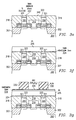
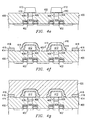
- Figure 3a-o illustrates in cross sectional elevation views the steps of first preferred embodiment fabrication methods for integrated circuits (e.g., CMOS or BiCMOS) with capacitors or memory cells (e.g., DRAM or FeRAM cells) as follows.
- integrated circuits e.g., CMOS or BiCMOS
- capacitors or memory cells e.g., DRAM or FeRAM cells
- the TiAlN hardmask 332 could be replaced with a hardmask of silicon dioxide or silicon nitride or silcon oxynitride; although the selectivity of the Pt etch will decrease. In this case an organic ARC layer would be used. A silicon dioxide or silicon nitride hardmask does not need the pre etch oxidation treatment.
- organic ARC oxygen plasma
- silicon oxide/nitride/oxynitride layer fluorine-based plasma
- TiAlN chlorine-based plasma
- strip the photoresist and organic ARC oxygen plasma
- N2 e.g., 10%
- An alternative Pt etch eliminates the hardmask and uses only a photoresist mask during a Cl2 RIE etch.
- photoresist-only mask etching of Pt with Cl2 leads to redeposition on the photoresist sidewall, forming a "fence" of residues which is difficult to remove.
- the preferred embodiment uses a two-step etch process. During the first step, performed with a Cl2 flow of 50 sccm at a pressure of 0.5 mTorr and a MW power of 1500 watts and RF power of 900 watts, etch the Pt (plus any adhesion layer) through to the underlying dielectric (e.g., oxide).
- This two-step preferred embodiment Pt etch could be used for lower density devices because the area enhancement is not as great as with steeper sidewalls, but the two-step process with only photoresist masking simplifies the Pt etch processing.
- This two-step etch could also be used for ferroelectric capacitor stack etches as described in subsequent preferred embodiments.
- a radiation source e.g., KrF excimer laser
- a radiation source can be mounted on the outside of the chamber and illuminate the wafer during etching.
- Anneals in hydrogen-containing atmospheres during CMOS processing can lead to degradation of BST, PZT, SBT, and other such materials.
- Pt electrodes have insufficient hydrogen diffusion barrier properties, but other materials such as PtOx, Ir, IrO2 Ru, RuO2, ... do provide hydrogen diffusion barriers.
- the resistivity of PtOx is at least an order of magnitude greater than that of Pt.
- Pt electrode for use with the foregoing preferred embodiments has a thin layer of PtOx at the interface of the BST, PZT, or SBT and the Pt.
- activated oxygen such as from a plasma in an ECR reactor.
- 1000 W of MW power and low power RF bias to create a plasma bias in the range of 0-100 volts
- a pressure of 10 mTorr and an oxygen flow of 100 sccm for 5 minutes This grows roughly 4-4.5 nm of PtOx when the wafer temperature is 64 C, but grows only about 3.7 nm of PtOx at 400 C and almost none at 650 C.
- the PtOx appears to be amorphous and primarily PtO2 with some PtO and thermally metastable.
- the oxidation appears to be self-limiting, and the 64 C oxidations yields a rougher surface than the 400 C oxidations.
- an analogous thin PtOx layer at the interface of the BST and the top Pt electrode can be formed by first sputtering a very thin (e.g., 2 nm) Pt layer and then completely oxidizing it with an oxygen plasma as just used to oxidize the surface of the bottom Pt electrode. Deposition of such a thin Pt layer requires low temperatures, and the Pt may not completely cover the surface. After the oxidation of the thin Pt layer, sputter deposit more Pt to complete the top Pt electrode.
- oxygen-containing plasmas can be used such as O2, O3, N2O, and combinations of these along with optional inert gasses.
- various types of reactors could be used to create the active oxygen for the Pt oxidation, including remote plasmas and photochemical assistance.
- the hydrogen barrier properties of PtOx can also protect the BST (or PZT or SBT) with the PtOx buried in the Pt electrode away from the interface with the BST.
- This imbedding the PtOx in the Pt electrode makes fabrication of the top Pt electrode simpler: deposit half of the top Pt, surface oxidize it as with the bottom electrode, and then deposit the other half of the top Pt.
- other multilayers of Pt and PtOx can be fabricated by in the same manner for use as electrodes.
- the PtOx can act as an oxygen source during a high temperature crystallization anneal of the BST.
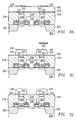
- Figures 4a-4h illustrate a capacitor-under-bitline version of the foregoing capacitor-over-bitline structure.
- Figure 4a shows vias formed
- Figure 4b illustrates the vias partially filled with doped polysilicon 404.
- the partial filling may be by a blanket deposition with etch back. This is analogous to Figure 3d showing polysilicon 320 filling vias.
- Figure 4c shows silicide 406 formed by blanket metal deposition followed by silicidation reaction and unreacted metal strip.
- Figure 4d illustrates diffusion barrier 408 analogous to diffusion barrier 322 of Figure 3e; the diffusion barrier may be made of TiAlN and formed by blanket deposition and planarization such as by CMP.
- Figure 4e illustrates platinum bottom electrodes 412 with adhesion TiAlN 410 after etching; this is analogous to Figure 3j.
- Figure 4f shows the BST 414, platinum top electrode 416, and top diffusion barrier 418 after patterning.
- the BST and top electrode may be common for all capacitors, and opening 419 is just at the location of the eventual bitline contact; opening 419 separates the top electrode from the eventual bitline contact 432.
- Figure 4g shows planarized dielectric 420.
- Figure 4h shows bitline 430 making contact 432 to the common drain of the transistors after contact etch and fill.
- the portion of bitline contact 432 through dielectric 400 could have been formed and filled (with polysilicon) simultaneously with the capacitor stems in Figures 4a-4d.
- the bitline contact through dielectric 420 would be a shallower and simpler to etch rather than through both dielectrics 400 and 420 at the same time.
- the foregoing etches of the Pt bottom electrodes may be adapted to etch materials such as Ir, Ru, ..., and their oxides (as described in the following sections) and used for DRAMs and FeRAMs but also may be adapted to etch materials such as FeNi, FeNiCo, NiCr, ... which are used in magnetic storage devices. That is, the N2 added to the plasma gasses and/or TiAlN or variant hardmasks used should improve sidewall slopes for essentially sputtering or ion milling etches with Ar and/or Cl.
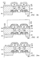
- Figures 6a-o illustrate in cross sectional elevation views the steps of second preferred embodiment fabrication methods for integrated circuits (e.g., CMOS or BiCMOS) with memory cells (e.g., FeRAM cells) as follows.
- integrated circuits e.g., CMOS or BiCMOS
- memory cells e.g., FeRAM cells
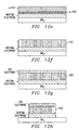
- FIG. 14 illustrates alternative onestep and two-step etches with photoresist (PR) mask through ILD (SiO2) and insulating diffusion barrier TiO2.
- PR photoresist
- the chemistries for the SiO 2 etch should contain a mixture of H- and F-containing gas, and an inert gas (e.g., He, Ne, Ar, Kr, Xe) can be used.
- an inert gas e.g., He, Ne, Ar, Kr, Xe
- the preferred chemistry for a particular reactor (AMAT P5000 RIE system) consisted of 15sccm CF 4 , 30 sccm CF 3 H and 100 sccm Ar flows to give a total process pressure of 100 mTorr.
- gases e.g., CH 2 F 2 , CH 3 F, CH 4 , C 2 F 6 , C 3 F 6 , C 3 F 8 , XeF 2 , NF 3 , SF 6
- gases e.g., CH 2 F 2 , CH 3 F, CH 4 , C 2 F 6 , C 3 F 6 , C 3 F 8 , XeF 2 , NF 3 , SF 6
- An etch chemistry which substitutes or adds compounds containing Cl, Br or I species will have similar properties.
- a combination of Cl- and F-containing species is used.
- Preferred embodiments include a Cl 2 /CF 4 /Ar mixture of the ratio 10/25/50 sccm or 25/25/5 sccm or a Cl 2 /O 2 /CF 4 /Ar mixture of the ratio 10/20/25/50 sccm.
- other gases can be substituted or added, such as other inert gases, or other sources of Cl, O or F (e.g., XeF 2 , NF 3 , SF 6 ).
- An etch chemistry which or adds or substitutes Br-containing species in place of the Cl-containing species will have similar properties. This etch can be also used for PZT of different compositions and doping, as well as other sidewall insulating diffusion barrier (Al 2 O 3 , AlN, etc.) or ferroelectric materials (e.g., SBT, BST).
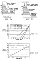
- Figure 15 illustrates the quadratic model for TiO 2 etch selectivity to photoresist. Non-linear dependences on Cl 2 fraction and the halogen fraction, expressed in terms of the Cl 2 and CF 4 flow (Cl 2 + CF 4 ), are seen. While the photoresist etch rate is not so sensitive to the change in conditions, the TiO 2 rate is greatest with high (although not 100%) halogen fraction. Predictions of the etch rates and selectivity for various Ar/Cl 2 /CF 4 mixtures shown in Figure 15 indicate that the most useful area of process space appears to be the lower two-thirds of the triangular mixture plot.
- the total process pressure is an important variable which provides additional control of etch rate and material selectivity. For example, high pressure operation (10 mTorr) increases chemical etching at the expense of physical sputtering, compared with low pressure conditions (0.5 mTorr).
- the plasma power(s) and plasma-substrate bias also control variables which can be used to adjust the process. These variables will depend on the reactor type that is employed. For the ECR-enhanced RIE reactor used for our demonstrations, we used pressures in the range 0.1 to 10 mTorr, microwave power from 300 to 1500 W and RF power from 0 to 900 W. The plasma bias under these conditions ranged from 0 (at 0 W applied RF power) to ⁇ -325 V (at 900 W RF power).
- the wafer temperature is another variable which will affect etch parameters. These etches described here used a He backside cooling in order to keep a low wafer temperature. Although the maximum temperature was not measured, photoresist on top of the wafer was still easily removed after etching. Increasing the wafer temperature will increase the component of chemical etching at the expense of sputter etching. It should then be possible to reduce the ion energies of the etch gas which will reduce the physical etch component and hence potentially improve the etch selectivities as well.
- etch reactors can be used to accomplish this etch, with suitable flow ratio and additive optimization, to improve selectivity and etch profile.
- Some examples are those with a single RF supply (such as inductively-coupled plasma (ICP) or parallel plate reactors) or dual RF supplies, or other enhanced plasma generation sources. While the system employed here uses 13.56 MHz rf and 2.45 GHz microwave generators, other plasma frequencies can be used with similar chemistries to those described here.
- etch endpoint can be accomplished in numerous ways, including optical emission spectroscopy (OES), mass spectrometry, or applied RF power sensing.
- OES optical emission spectroscopy
- material-specific signatures have been determined for SiO 2 (483.5 nm) and TiO 2 etching (322, 335, 364, 375, 415 and 430nm).
- Additional wet-etch or recovery anneal steps may also be used to remove etch damage layers, as appropriate.
- Ir electrodes either bottom or top or both of the foregoing capacitors could be replaced with Ir plus IrO2 layers in order to have an oxygen source to deter oxygen depletion during crystallization anneals.
- a preferred embodiment method of making alternating layers of Ir and IrO2 first deposits Ir (e.g., sputter deposit 50 nm), then oxidize the surface of the Ir with an oxygen plasma to grow about 3 nm of IrO2.
- Another layer of Ir can be deposited by further sputter deposition, and another oxidation can be performed. In this manner any number of alternating Ir and IrO2 layers can be made.
- a thin Ir layer can be entirely oxidized, so a stack can begin and end with either Ir or IrO2.
- Plasma oxidation appears to give smoother IrO2 surfaces than furnace oxidation and at a much lower temperature.
- Ir and IrO2 layers are possible electrodes; in particular, the following: Ir/PZT/IrO2, IrO2/PZT/Ir, Ir/PZT/IrO2/Ir, Ir/PZT/Ir/IrO2/Ir, Ir/IrO2/PZT/IrO2/Ir, Ir/IrO2/PZT/Ir/IrO2/Ir, Ir/IrO2/Ir/PZT/IrO2/Ir, Ir/IrO2/Ir/PZT/Ir/IrO2/Ir.
- top and bottom electrodes such as noble metals (Ir, Pt, Ru, Rh, Pd, Pt, Ag, Au) or conducting oxides such as IrO2, RuO2, PdO, RhO2, SrRuO3, LaSrCoO3, YBa2Cu3O7, etc. or multiple layers or alloys of these materials.
- noble metals Ir, Pt, Ru, Rh, Pd, Pt, Ag, Au
- conducting oxides such as IrO2, RuO2, PdO, RhO2, SrRuO3, LaSrCoO3, YBa2Cu3O7, etc. or multiple layers or alloys of these materials.
- the ferroelectric material needs to be smooth with a uniform grain structure.
- Small grain size is important in obtaining smooth surfaces. Smooth surfaces are needed in order to have a uniform electric field through the ferroelectric film as well as maintaining a low leakage current through the film. Thickness non-uniformities also degrade reliability because they create regions with large electric fields.
- Standard thermal MOCVD PZT has fairly large grain size (roughly 100 nm diameter) and rough surfaces (peak-to-valley variation of roughly 40 nm).
- the preferred embodiments enhance nucleation density with approaches which include: (1) Use plasma pre-treatment of the bottom electrode prior to thermal MOCVD or plasma-enhanced MOCVD ferroelectric deposition. (2) Use an initial growth step of plasma-enhanced MOCVD ferroelectric deposition prior to thermal MOCVD ferroelectric deposition. (3) Use plasma pre-treatment of the bottom electrode prior to sputtered or reactive sputtered ferroelectric deposition.
- FIGs 11a-11d A heuristic illustration of how low nucleation density impacts roughness and grain size is shown in Figures 11a-11d. These figures assume that nuclei grow three dimensionally with a roughly isotropic growth rate. SBT when grown in the crystalline phase will form in a very non-isotropic facetted manner. This will result in similar trends but different quantitative relationships between average film thickness, grain size, and surface roughness. Nucleation occurs randomly at the start as per Figure 11a. During growth the nuclei grow until they impinge on each other, at which point grain boundaries are formed as in Figure 11b. As the film becomes thicker the grains finally cover the surface of the film as shown by Figure 11c.
- the preferred embodiment treatment of the bottom electrode essentially textures the bottom electrode surface to provide more nucleation sites and thus a larger nucleation density.
- an oxygen plasma treatment may even grow metal oxide on the electrode surface.
- Various process methods to implement plasma pre-treatment of the bottom electrode are as follows.
- Process methods to implement plasma enhanced MOCVD of the ferroelectric for the seed layer are as follows.
- the RF plasma Prior to thermal MOCVD the RF plasma is turned on with Ar and/or O 2 gas flowing into the chamber.
- the RF energy might be either remote and / or applied to the wafer surface.
- the precursors are then turned on into the deposition chamber.
- the MOCVD process parameters for the plasma-enhanced process need to be optimized separately from the thermal MOCVD process. Therefore the pressure, carrier flows, oxidizer flows, liquid flows and perhaps liquid composition can be different from the thermal MOCVD process values.
- the plasma bias could be about 100 volts and the duration only seconds to insure at least partial surface coverage and high nucleation density.
- the preferred embodiment grain structure control provides an amorphous lead titanate buffer layer prior to the PZT deposition.
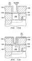
- Figure 12a shows a bottom electrode on oxide, the bottom electrode could be Ir, Pt, IrO2, etc.
- Figure 12b shows a thin (5 nm) layer of Ti (or TiO2) formed on the bottom electrode, such as by CVD, sputtering, or e-beam evaporation.
- Figures 12c-12d illustrates sputtering PbO (or Pb) into the Ti (or TiO2) to form an amorphous PbTiO3 (a-PTO) layer containing 10-20% excess Pb atoms (over stoichiometric) and having a thickness of about 8 nm.
- Figure 12e shows 250 nm thick layer of amorphous PZT (a-PZT) formed on the a-PTO by cosputtering Pb(Zr 0.5 Ti 0.5 )O 3 and PbO targets at 200 C.
- the PZT was crystallized at 500 C (instead of 520 C required without the PTO seed layer) or by rapid thermal annealing at 600 C in an oxygen atmosphere for 20 seconds (Figure 12f).
- Figure 12g shows deposition of top electrode (Ir, Pt, IrO2, etc.) by sputtering or e-beam evaporation.
- Figure 12h illustrates the stack etch to form the ferroelectric capacitor.
- the PZT ferroelectric could be replaced by other perovskite ferroelectrics such as doped PZT, PZT with the lead replaced (at least in part) by Ca, Sr, Ba, Na, Li, K, La, Ce, Bi or combinations, PZT with the Zr and/or Ti replaced (at least in part) by Zr, Ti, Hf, Ta, Nb, Mn, Fe, Co, Ni, Al or combinations, and combinations of the replacements.
- Layered perovskites such as Bi4Ti3O12, SrBi2(Ta,Nb)O9, etc. may also be used. Further, paraelectric versions of these materials could be used for the dielectric of the first preferred embodiments.
- step (6)-(7) above An alternative to the sidewall diffusion barrier formation by deposition and anisotropic etching (steps (6)-(7) above) proceeds as follows. First conformally deposit metal such as titanium or aluminum to a thickness of 10-20 nm on the capacitor and dielecctric; next, anisotropically etch the metal to leave a metal sidewall; and, lastly, oxidizes the metal to form the sidewall insulating diffusion barrier of TiO2 or Al2O3. Oxidize the metal sidewall with a low temperature (50 C) oxygen plasma (10 Torr pressure and 100 V plasma bias); this avoids also oxidizing exposed TiAlN.
- metal such as titanium or aluminum
- This sidewall alternative allows use of an anisotropic metal etch which can be more selective to the other insulators than the anisotropic insulating diffusion barrier etch.
- the conformal metal deposition may be by TiCl4 thermal decomposition or sputtering Ti or Al to avoid hydrogen generation.
- the anisotropic etches may be plasmas of BCl3 and Cl2.
- the foregoing preferred embodiments may be varied by using a thick (e.g., 200 nm) top TiAlN diffusion barrier also as the hardmask and eliminating the oxide hardmask.
- a thick (e.g., 200 nm) top TiAlN diffusion barrier also as the hardmask and eliminating the oxide hardmask.
- the photoresist is stripped after the TiAlN top etch but prior to the Ir etch by switching to a gas flow of 92 sccm O2 and 8 sccm N2 at a pressure of 10 mTorr and 1500 W of MW power but 0 plasma bias.
- the top TiAlN will survive the bottom TiAlN strip due to its thickness.
- the Ir and PZT etches may have N2 added to help deter hardmask erosion as with the previously described Pt etch of the first preferred embodiments.
- TiAlN/Ir/PZT/Ir/TiAlN capacitor stack and diffusion barrier materials and plasma etches may be modified in various ways including the following.
- the Cl2 etch can have O2 and N2 added; the O2 and N2 deter erosion of hardmasks such as TiAlN, but oxygen will erode softmasks.
- the N2 modifies the noble metal and helps increase sidewall slope.
- other gasses can be the sources of the Cl, O, and N species, such as OCl2, N2O, ... .
- Other halogens (Br and I) could also be used in place of or in addition to the Cl.
- the Cl2+CF4+Ar etch can have O2 added and the mixture varied; the O2 addition helps deter loss of oxygen from the PZT.
- other gasses can be the sources of the Cl, F, Ar, and O species, such as OCl2, ClF2, ... .
- the Ar breaks the PZT bonds allowing the Cl and F to react to form volatiles products with the Pb, Zr, and Ti.
- the relative volatilities of the fluorides and chlorides vary for Pb, Zr, and Ti; so the composition of the PZT (Zr to Ti ratio) leads to selection of the F to Cl ratio.
- the low pressure, high bias Cl2 plasma etch can be replaced with a low pressure (0.5 mTorr), high bias (ECR reactor with 1500 W MW power and 900 W RF bias power) plasma of Cl2 (10 sccm), CF4 (25 sccm), and Ar (50 sccm). Adding oxygen to this barrier etch yields the PZT etch; this provides convenient multistep etches.
- the etch process for each layer has a reasonable selectivity for the underlying layers. This allows the use of a more liberal overetch of each layer prior to etching subsequent layers. This overetch will help compensate for non-uniformity in etch rates across the wafer. Under the best case conditions, the non-uniformity of the final etch will be only a little worse than the nonuniformity in the etch process of the last material and not be a combined total of all of the etch processes.
- a large overetch is also desirable. This overetch can only be done if the selectivity between the hardmask and etched material is large. In addition, a large selectivity to the underlying materials is necessary for a large overetch.
- hardmask materials are very dependent on etch chemistries, etch processes and resulting etch selectivities.
- the choice of electrode materials and ferroelectrics is usually determined by optimum properties.
- the optimum hardmask material is simple to deposit, can be chemically etched to achieve sharp profile yet under etch conditions that work well for underlying materials etches has a good selectivity (low etch rate).
- the hardmask must also either be easily removed or must be useful or at least not cause problems for further processing.
- Etch recipes used to demonstrate etch selectivities were used to demonstrate etch selectivities.
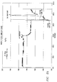
- Figure 9a illustrates the optical emission spectroscopy (OES) signals for an Ir/PZT/Ir stack etch with a 20-second off time for the plasma during gas mixture shifts.
- the Ir etch is Cl2 and the PZT etch is Cl2+CF4+Ar+O2, and both Ir and PZT related OES signals are monitored.
- the changes in OES signals determine etch step endpoint, and the preferred embodiments then add a timed overetch followed by a plasma off time for gas mixture switching and then plasma reignition and the next etch step. This allows automatic process control.
- Figure 9b shows the OES signals that occur during the Ir etch step under two different chemistries.
- Light emission occurs during plasma etching as, for instance, etch products are excited by electrons or ions in the plasma.
- Two Ir emission bands (350-352 nm and 378-380 nm) are available, and can be further enhanced with various background subtraction techniques:
- Figure 9c illustrates the during and after Ir etch spectra, and Figure 9d the 380 nm intensity minus the 381.4 nm intensity as a function of time about the endpoint. The large change of the background subtracted signal clearly indicates the endpoint.
- emission wavelengths can be very sensitive to particuarl etching materials (e.g., 380 nm for Ir etching in Cl2 chemistries), while others are not.
- Other wavelengths are indirectly related to the etched species (e.g., CO emission at 438.5 nm during oxide etch), but are still useful process monitors.
- Figure 9e illustrates OES traces for five emission lines during a stack etch in which the photoresist used to mask the hardmask etch (TiAlN HM Etch) is stripped (PR Ash).
- TiAlN HM Etch hardmask etch
- PR Ash PR Ash
- the TiAlN etch endpoint is on the TiAlN and Ir (top electrode) signals
- the photoresist ash is timed
- the Ir top electrode endoint is on the Ir and PZT signals
- the PZT etch endoint is on the PZT and Ir (bottom electrode) signals.
- the RF harmonics could be used for endpoint detection analogous to Figure 5b.
- reflectometry or spectral reflectometry or mass spectrometry could be used for endpoint detection.
- these endpoint detection methods sense one of: (1) the gas environment (OES, mass spectrometry), (2) the plasma characteristics (RF power harmonics, electron energy distribution, discharge current), and (3) etched wafer characteristics (reflectormetry).
- OES gas environment
- RF power harmonics RF power harmonics
- RF current harmonics etched wafer characteristics
- a softmask photoresist only mask on Ir/PZT/Ir or Pt/SBT/Pt stacks
- two-step etch may be used.
- photoresist-only mask etching of Pt or Ir with Cl2 plus etching PZT or SBT with Cl2 plus O2 leads to redeposition on the photoresist sidewall, forming the fence of residues which is difficult to remove.
- the preferred embodiment softmask stack etch uses a two-step etch process.
- the first step performed at a pressure of 0.5 mTorr and a MW power of 1500 watts and RF power of 900 watts, etch the top Pt or Ir with Cl2 at 50 sccm, next etch the PZT or SBT with Cl2 at 25 sccm plus O2 at 25 sccm, then etch the bottom Pt or Ir again with Cl2 at 50 sccm through to the underlying dielectric (e.g., oxide). Then increase the pressure to about 10 mTorr and continue for a 20% overetch. The higher pressure leads to an enhanced photoresist removal rate, which, in turn, serves to remove the residue fence. This approach yields sidewall slopes about 60 degrees with no fence using standard photoresist processing.
- This two-step etch has the advantages of omitting the hardmask layer deposition and etch steps while still providing a sufficiently steep sidewall so that the self-aligned diffusion barrier as previously described in connection with Figures 7a-7d can be formed.
- the second preferred embodiments adapt to a capacitor under bitline structure fabricated in a manner analogous to that illustrated in Figures 4a-4h.
- capacitor stems 1020 plus also bitline stems 1021 as illustrated in Figure 10a first form capacitor stems 1020 plus also bitline stems 1021 as illustrated in Figure 10a.
- FIG. 10b illustrates the silicon oxynitride hardmask case.
- interlevel dielectric 1050 and form drive lines with a dual damascene process as follows. First etch vias down to the bitline stems and capacitor top electrodes (through any insulating hardmasks on the top electrodes). Then etch trenches for drive lines which parallel the word lines. Lastly, fill the vias and trenches with metal (diffusion barriers plus copper) and planarize with CMP to form the drive lines 1060 and filled vias 1062 to the bitline stems; see Figure 10c.
- bitlines 1070 Deposit interlevel dielectric 1070 and form bitlines with a dual damascene process as follows. First etch vias down to the filled vias on the bitline stems. Then etch trenches for bitlines which are perpendicular to the drive lines and the word lines. Lastly, fill the vias and trenches with metal (diffusion barriers plus copper) and planarize with CMP to form the bitlines 1080; see Figure 10d.
- Figure 8 illustrates in cross sectional elevation views the new step of third preferred embodiments methods for fabrication of integrated circuits (e.g., CMOS or BiCMOS) with capacitors or memory cells (e.g., FeRAM cells) as follows.
- integrated circuits e.g., CMOS or BiCMOS
- capacitors or memory cells e.g., FeRAM cells
- Step (3) of the foregoing provided for bismuth infusion into the Pt bottom electrode prior to deposition of SBT.
- An alternative to the spin coating method would be to transport Bi by gas phase; that is, use MOCVD to deposit Bi on Pt bottom electrode and diffuse the Bi into the Pt by an anneal. Afterwards, any residual Bi compounds can be stripped in an acid solution. Also, annealing in an atmosphere saturated with Bi could be direct gas phase doping of the Pt. Bi has a vapor pressure of about 20 mTorr at 700 C.
- the bottom electrode could have a composition on the order of 1% Bi.
- the co-sputtering may be replaced by a simpler sequential sputtering process: sputter 10-20 nm Pt, then 1 nm Bi (full coverage is not necessary, this is just an average thickness), then 10-20 nm Pt. In this case the Bi diffuses in the Pt during SBT recrystallization.
- An alternative embodiment provides a Bi atmosphere for the recrystallization anneal of the SBT; this helps maintain the stoichiometry of the SBT against Bi evaporation.
- Alternative preferred embodiments add to or replace the Bi atmosphere as follows:
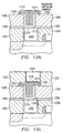
- Figures 13a-13h Illustrate a fourth preferred embodiment PZT or SBT capacitor extending in three dimensions in the shape of a cup instead of the planar capacitors of Figures 6a-6f, 10a-10d.
- the fourth preferred embodiment may be fabricated as follows.
- the preferred embodiments can be modified in various ways while retaining the features of a multistep via etch through dielectric plus insulating diffusion barrier.
Landscapes
- Engineering & Computer Science (AREA)
- Manufacturing & Machinery (AREA)
- Semiconductor Memories (AREA)
- Semiconductor Integrated Circuits (AREA)
- Internal Circuitry In Semiconductor Integrated Circuit Devices (AREA)
- Drying Of Semiconductors (AREA)
Applications Claiming Priority (8)
| Application Number | Priority Date | Filing Date | Title |
|---|---|---|---|
| US9957198P | 1998-09-09 | 1998-09-09 | |
| US99571P | 1998-09-09 | ||
| US9984898P | 1998-09-11 | 1998-09-11 | |
| US99848P | 1998-09-11 | ||
| US11422898P | 1998-12-30 | 1998-12-30 | |
| US114228P | 1998-12-30 | ||
| US12368799P | 1999-03-10 | 1999-03-10 | |
| US123687P | 1999-03-10 |
Publications (3)
| Publication Number | Publication Date |
|---|---|
| EP1001459A2 true EP1001459A2 (fr) | 2000-05-17 |
| EP1001459A3 EP1001459A3 (fr) | 2000-09-20 |
| EP1001459B1 EP1001459B1 (fr) | 2011-11-09 |
Family
ID=27493068
Family Applications (1)
| Application Number | Title | Priority Date | Filing Date |
|---|---|---|---|
| EP99202911A Expired - Lifetime EP1001459B1 (fr) | 1998-09-09 | 1999-09-09 | Circuit integré avec condensateur et son procédé de fabrication |
Country Status (4)
| Country | Link |
|---|---|
| US (3) | US6211035B1 (fr) |
| EP (1) | EP1001459B1 (fr) |
| JP (1) | JP2000133633A (fr) |
| AT (1) | ATE533178T1 (fr) |
Cited By (12)
| Publication number | Priority date | Publication date | Assignee | Title |
|---|---|---|---|---|
| WO2000049202A3 (fr) * | 1999-02-17 | 2000-12-28 | Applied Materials Inc | Procedes de gravure ameliores pour profil de platine anisotrope |
| WO2002059976A1 (fr) * | 2001-01-24 | 2002-08-01 | Infineon Technologies North America Corp. | Procede de fabrication d'un dispositif memoire a semi-conducteurs |
| DE19942119C2 (de) * | 1999-09-03 | 2002-08-08 | Mosel Vitelic Inc | Oberflächenbehandlung für eine Metallschicht |
| WO2002069378A1 (fr) * | 2001-02-27 | 2002-09-06 | Infineon Technologies Ag | Procede pour enlever une couche de masquage d'un substrat semi-conducteur |
| US6482745B1 (en) | 1998-01-13 | 2002-11-19 | Applied Materials, Inc. | Etching methods for anisotropic platinum profile |
| WO2003012838A1 (fr) * | 2001-07-31 | 2003-02-13 | Applied Materials, Inc. | Procede d'attaque de couches conductrices pour condensateur et fabrication de dispositifs a semi-conducteur |
| WO2003012851A3 (fr) * | 2001-07-31 | 2003-04-24 | Applied Materials Inc | Procede de gravure de couches ferroelectriques |
| WO2003103027A1 (fr) * | 2002-06-04 | 2003-12-11 | Infineon Technologies Ag | Procede permettant de former un contact pour un condensateur |
| US7055263B2 (en) | 2003-11-25 | 2006-06-06 | Air Products And Chemicals, Inc. | Method for cleaning deposition chambers for high dielectric constant materials |
| EP1341220A3 (fr) * | 2002-02-28 | 2007-08-01 | Fujitsu Limited | Procédé de fabrication d'un dispositif semiconducteur |
| US7285490B2 (en) | 2003-01-15 | 2007-10-23 | Infineon Technologies Ag | Method for the producing an integrated circuit bar arrangement, in particular comprising a capacitor assembly, in addition to an integrated circuit arrangement |
| US7357138B2 (en) | 2002-07-18 | 2008-04-15 | Air Products And Chemicals, Inc. | Method for etching high dielectric constant materials and for cleaning deposition chambers for high dielectric constant materials |
Families Citing this family (236)
| Publication number | Priority date | Publication date | Assignee | Title |
|---|---|---|---|---|
| US6333066B1 (en) * | 1997-11-21 | 2001-12-25 | Samsung Electronics Co., Ltd. | Method for forming PZT thin film using seed layer |
| JP3381774B2 (ja) * | 1997-12-24 | 2003-03-04 | 東京エレクトロン株式会社 | CVD−Ti膜の成膜方法 |
| US6972436B2 (en) * | 1998-08-28 | 2005-12-06 | Cree, Inc. | High voltage, high temperature capacitor and interconnection structures |
| JP2000133633A (ja) * | 1998-09-09 | 2000-05-12 | Texas Instr Inc <Ti> | ハ―ドマスクおよびプラズマ活性化エッチャントを使用した材料のエッチング方法 |
| JP3931445B2 (ja) * | 1998-09-10 | 2007-06-13 | 株式会社日立製作所 | 半導体装置の製造方法 |
| US6218293B1 (en) * | 1998-11-13 | 2001-04-17 | Micron Technology, Inc. | Batch processing for semiconductor wafers to form aluminum nitride and titanium aluminum nitride |
| US6204178B1 (en) * | 1998-12-29 | 2001-03-20 | Micron Technology, Inc. | Nucleation and deposition of PT films using ultraviolet irradiation |
| US6387748B1 (en) | 1999-02-16 | 2002-05-14 | Micron Technology, Inc. | Semiconductor circuit constructions, capacitor constructions, and methods of forming semiconductor circuit constructions and capacitor constructions |
| US6265262B1 (en) * | 1999-06-02 | 2001-07-24 | Matsushita Electric Industrial Co., Ltd. | Semiconductor device and method of fabricating the same |
| KR20010001924A (ko) * | 1999-06-09 | 2001-01-05 | 김영환 | 반도체소자의 커패시터 제조방법 |
| KR100309077B1 (ko) * | 1999-07-26 | 2001-11-01 | 윤종용 | 삼중 금속 배선 일 트랜지스터/일 커패시터 및 그 제조 방법 |
| US7554829B2 (en) | 1999-07-30 | 2009-06-30 | Micron Technology, Inc. | Transmission lines for CMOS integrated circuits |
| JP4381526B2 (ja) * | 1999-10-26 | 2009-12-09 | 東京エレクトロン株式会社 | プラズマエッチング方法 |
| US6485988B2 (en) * | 1999-12-22 | 2002-11-26 | Texas Instruments Incorporated | Hydrogen-free contact etch for ferroelectric capacitor formation |
| US6534809B2 (en) * | 1999-12-22 | 2003-03-18 | Agilent Technologies, Inc. | Hardmask designs for dry etching FeRAM capacitor stacks |
| KR100328450B1 (ko) * | 1999-12-29 | 2002-03-16 | 박종섭 | 반도체 소자의 캐패시터 제조방법 |
| KR20010059284A (ko) * | 1999-12-30 | 2001-07-06 | 박종섭 | 반도체 소자의 캐패시터 형성방법 |
| JP3976462B2 (ja) * | 2000-01-26 | 2007-09-19 | エルピーダメモリ株式会社 | 半導体装置の製造方法 |
| GB2361244B (en) | 2000-04-14 | 2004-02-11 | Trikon Holdings Ltd | A method of depositing dielectric |
| US6436838B1 (en) * | 2000-04-21 | 2002-08-20 | Applied Materials, Inc. | Method of patterning lead zirconium titanate and barium strontium titanate |
| US6455326B1 (en) * | 2000-05-15 | 2002-09-24 | Ramtron International Corporation | Enhanced process capability for sputtered ferroelectric films using low frequency pulsed DC and RF power supplies |
| US6573167B2 (en) * | 2000-08-10 | 2003-06-03 | Texas Instruments Incorporated | Using a carbon film as an etch hardmask for hard-to-etch materials |
| US6787833B1 (en) * | 2000-08-31 | 2004-09-07 | Micron Technology, Inc. | Integrated circuit having a barrier structure |
| US6682969B1 (en) * | 2000-08-31 | 2004-01-27 | Micron Technology, Inc. | Top electrode in a strongly oxidizing environment |
| US7067176B2 (en) | 2000-10-03 | 2006-06-27 | Cree, Inc. | Method of fabricating an oxide layer on a silicon carbide layer utilizing an anneal in a hydrogen environment |
| US6610366B2 (en) | 2000-10-03 | 2003-08-26 | Cree, Inc. | Method of N2O annealing an oxide layer on a silicon carbide layer |
| US6956238B2 (en) | 2000-10-03 | 2005-10-18 | Cree, Inc. | Silicon carbide power metal-oxide semiconductor field effect transistors having a shorting channel and methods of fabricating silicon carbide metal-oxide semiconductor field effect transistors having a shorting channel |
| US6767843B2 (en) * | 2000-10-03 | 2004-07-27 | Cree, Inc. | Method of N2O growth of an oxide layer on a silicon carbide layer |
| US6521529B1 (en) * | 2000-10-05 | 2003-02-18 | Advanced Micro Devices, Inc. | HDP treatment for reduced nickel silicide bridging |
| JP4666740B2 (ja) * | 2000-10-06 | 2011-04-06 | 川崎マイクロエレクトロニクス株式会社 | 半導体製造装置、被処理基板表面の処理方法およびプラズマ生成物の付着状態の観察方法 |
| US6737728B1 (en) * | 2000-10-12 | 2004-05-18 | Intel Corporation | On-chip decoupling capacitor and method of making same |
| US6958508B2 (en) | 2000-10-17 | 2005-10-25 | Matsushita Electric Industrial Co., Ltd. | Ferroelectric memory having ferroelectric capacitor insulative film |
| JP4829678B2 (ja) * | 2000-10-17 | 2011-12-07 | パナソニック株式会社 | 強誘電体メモリ及びその製造方法 |
| US6627463B1 (en) * | 2000-10-19 | 2003-09-30 | Applied Materials, Inc. | Situ measurement of film nitridation using optical emission spectroscopy |
| US6458722B1 (en) * | 2000-10-25 | 2002-10-01 | Applied Materials, Inc. | Controlled method of silicon-rich oxide deposition using HDP-CVD |
| US6740603B2 (en) * | 2001-02-01 | 2004-05-25 | Texas Instruments Incorporated | Control of Vmin transient voltage drift by maintaining a temperature less than or equal to 350° C. after the protective overcoat level |
| US7132219B2 (en) * | 2001-02-02 | 2006-11-07 | Brewer Science Inc. | Polymeric antireflective coatings deposited by plasma enhanced chemical vapor deposition |
| US6852167B2 (en) | 2001-03-01 | 2005-02-08 | Micron Technology, Inc. | Methods, systems, and apparatus for uniform chemical-vapor depositions |
| US6900498B2 (en) * | 2001-05-08 | 2005-05-31 | Advanced Technology Materials, Inc. | Barrier structures for integration of high K oxides with Cu and Al electrodes |
| JP2002353414A (ja) * | 2001-05-22 | 2002-12-06 | Oki Electric Ind Co Ltd | 誘電体キャパシタおよびその製造方法 |
| US6828162B1 (en) * | 2001-06-28 | 2004-12-07 | Advanced Micro Devices, Inc. | System and method for active control of BPSG deposition |
| US6727140B2 (en) * | 2001-07-11 | 2004-04-27 | Micron Technology, Inc. | Capacitor with high dielectric constant materials and method of making |
| US8026161B2 (en) | 2001-08-30 | 2011-09-27 | Micron Technology, Inc. | Highly reliable amorphous high-K gate oxide ZrO2 |
| US6844203B2 (en) | 2001-08-30 | 2005-01-18 | Micron Technology, Inc. | Gate oxides, and methods of forming |
| TWI276153B (en) * | 2001-11-12 | 2007-03-11 | Hynix Semiconductor Inc | Method for fabricating semiconductor device |
| KR100422597B1 (ko) * | 2001-11-27 | 2004-03-16 | 주식회사 하이닉스반도체 | 다마신 공정에 의해 형성된 캐패시터와 금속배선을 가지는반도체소자 |
| US20040259316A1 (en) * | 2001-12-05 | 2004-12-23 | Baki Acikel | Fabrication of parallel plate capacitors using BST thin films |
| WO2003052781A1 (fr) * | 2001-12-14 | 2003-06-26 | Midwest Research Institute | Circuit accordable pour dispositifs de condensateurs accordables |
| US6953730B2 (en) | 2001-12-20 | 2005-10-11 | Micron Technology, Inc. | Low-temperature grown high quality ultra-thin CoTiO3 gate dielectrics |
| US6900122B2 (en) * | 2001-12-20 | 2005-05-31 | Micron Technology, Inc. | Low-temperature grown high-quality ultra-thin praseodymium gate dielectrics |
| US6635498B2 (en) | 2001-12-20 | 2003-10-21 | Texas Instruments Incorporated | Method of patterning a FeRAM capacitor with a sidewall during bottom electrode etch |
| US6713342B2 (en) * | 2001-12-31 | 2004-03-30 | Texas Instruments Incorporated | FeRAM sidewall diffusion barrier etch |
| US6773930B2 (en) * | 2001-12-31 | 2004-08-10 | Texas Instruments Incorporated | Method of forming an FeRAM capacitor having a bottom electrode diffusion barrier |
| US6767750B2 (en) | 2001-12-31 | 2004-07-27 | Texas Instruments Incorporated | Detection of AIOx ears for process control in FeRAM processing |
| US7067235B2 (en) * | 2002-01-15 | 2006-06-27 | Ming Huan Tsai | Bi-layer photoresist dry development and reactive ion etch method |
| US6767795B2 (en) * | 2002-01-17 | 2004-07-27 | Micron Technology, Inc. | Highly reliable amorphous high-k gate dielectric ZrOXNY |
| US20030143853A1 (en) * | 2002-01-31 | 2003-07-31 | Celii Francis G. | FeRAM capacitor stack etch |
| US7129178B1 (en) | 2002-02-13 | 2006-10-31 | Cypress Semiconductor Corp. | Reducing defect formation within an etched semiconductor topography |
| JP2003243630A (ja) * | 2002-02-18 | 2003-08-29 | Sony Corp | 磁気メモリ装置およびその製造方法 |
| US6806095B2 (en) * | 2002-03-06 | 2004-10-19 | Padmapani C. Nallan | Method of plasma etching of high-K dielectric materials with high selectivity to underlying layers |
| US20060252265A1 (en) * | 2002-03-06 | 2006-11-09 | Guangxiang Jin | Etching high-kappa dielectric materials with good high-kappa foot control and silicon recess control |
| US20030176073A1 (en) * | 2002-03-12 | 2003-09-18 | Chentsau Ying | Plasma etching of Ir and PZT using a hard mask and C12/N2/O2 and C12/CHF3/O2 chemistry |
| US6812100B2 (en) * | 2002-03-13 | 2004-11-02 | Micron Technology, Inc. | Evaporation of Y-Si-O films for medium-k dielectrics |
| JP4090766B2 (ja) * | 2002-03-19 | 2008-05-28 | 富士通株式会社 | 半導体装置の製造方法 |
| JP2003289134A (ja) * | 2002-03-28 | 2003-10-10 | Matsushita Electric Ind Co Ltd | 半導体装置及びその製造方法 |
| US7160577B2 (en) | 2002-05-02 | 2007-01-09 | Micron Technology, Inc. | Methods for atomic-layer deposition of aluminum oxides in integrated circuits |
| US7045430B2 (en) | 2002-05-02 | 2006-05-16 | Micron Technology Inc. | Atomic layer-deposited LaAlO3 films for gate dielectrics |
| US7589029B2 (en) | 2002-05-02 | 2009-09-15 | Micron Technology, Inc. | Atomic layer deposition and conversion |
| US7094704B2 (en) * | 2002-05-09 | 2006-08-22 | Applied Materials, Inc. | Method of plasma etching of high-K dielectric materials |
| US6686293B2 (en) * | 2002-05-10 | 2004-02-03 | Applied Materials, Inc | Method of etching a trench in a silicon-containing dielectric material |
| JP3883470B2 (ja) | 2002-05-14 | 2007-02-21 | 沖電気工業株式会社 | 半導体装置の製造方法 |
| US7205218B2 (en) | 2002-06-05 | 2007-04-17 | Micron Technology, Inc. | Method including forming gate dielectrics having multiple lanthanide oxide layers |
| US7135421B2 (en) | 2002-06-05 | 2006-11-14 | Micron Technology, Inc. | Atomic layer-deposited hafnium aluminum oxide |
| US7154140B2 (en) * | 2002-06-21 | 2006-12-26 | Micron Technology, Inc. | Write once read only memory with large work function floating gates |
| US6804136B2 (en) * | 2002-06-21 | 2004-10-12 | Micron Technology, Inc. | Write once read only memory employing charge trapping in insulators |
| US7193893B2 (en) * | 2002-06-21 | 2007-03-20 | Micron Technology, Inc. | Write once read only memory employing floating gates |
| US6902681B2 (en) * | 2002-06-26 | 2005-06-07 | Applied Materials Inc | Method for plasma etching of high-K dielectric materials |
| US7221017B2 (en) * | 2002-07-08 | 2007-05-22 | Micron Technology, Inc. | Memory utilizing oxide-conductor nanolaminates |
| US7221586B2 (en) | 2002-07-08 | 2007-05-22 | Micron Technology, Inc. | Memory utilizing oxide nanolaminates |
| US20040007561A1 (en) * | 2002-07-12 | 2004-01-15 | Applied Materials, Inc. | Method for plasma etching of high-K dielectric materials |
| US20040011380A1 (en) * | 2002-07-18 | 2004-01-22 | Bing Ji | Method for etching high dielectric constant materials and for cleaning deposition chambers for high dielectric constant materials |
| US20040014327A1 (en) * | 2002-07-18 | 2004-01-22 | Bing Ji | Method for etching high dielectric constant materials and for cleaning deposition chambers for high dielectric constant materials |
| US6664168B1 (en) * | 2002-07-24 | 2003-12-16 | Intel Corporation | Method of making an on-die decoupling capacitor for a semiconductor device |
| US6921702B2 (en) | 2002-07-30 | 2005-07-26 | Micron Technology Inc. | Atomic layer deposited nanolaminates of HfO2/ZrO2 films as gate dielectrics |
| US6790791B2 (en) * | 2002-08-15 | 2004-09-14 | Micron Technology, Inc. | Lanthanide doped TiOx dielectric films |
| US6884739B2 (en) | 2002-08-15 | 2005-04-26 | Micron Technology Inc. | Lanthanide doped TiOx dielectric films by plasma oxidation |
| US20040036129A1 (en) * | 2002-08-22 | 2004-02-26 | Micron Technology, Inc. | Atomic layer deposition of CMOS gates with variable work functions |
| US6967154B2 (en) * | 2002-08-26 | 2005-11-22 | Micron Technology, Inc. | Enhanced atomic layer deposition |
| US7199023B2 (en) * | 2002-08-28 | 2007-04-03 | Micron Technology, Inc. | Atomic layer deposited HfSiON dielectric films wherein each precursor is independendently pulsed |
| US7084078B2 (en) * | 2002-08-29 | 2006-08-01 | Micron Technology, Inc. | Atomic layer deposited lanthanide doped TiOx dielectric films |
| US7022378B2 (en) * | 2002-08-30 | 2006-04-04 | Cree, Inc. | Nitrogen passivation of interface states in SiO2/SiC structures |
| US6841458B2 (en) * | 2002-09-12 | 2005-01-11 | Intel Corporation | Dopant interface formation |
| US8349241B2 (en) | 2002-10-04 | 2013-01-08 | Molecular Imprints, Inc. | Method to arrange features on a substrate to replicate features having minimal dimensional variability |
| US20040072442A1 (en) * | 2002-10-15 | 2004-04-15 | Francis Gabriel Celii | Low-bias bottom electrode etch for patterning ferroelectric memory elements |
| US7183120B2 (en) * | 2002-10-31 | 2007-02-27 | Honeywell International Inc. | Etch-stop material for improved manufacture of magnetic devices |
| EP1420451A3 (fr) * | 2002-11-13 | 2007-10-03 | Matsushita Electric Industrial Co., Ltd. | Dispositif de mémoire à semi-conducteurs non-volatile et son procédé de fabrication |
| TWI229935B (en) * | 2002-11-13 | 2005-03-21 | Matsushita Electric Industrial Co Ltd | Semiconductor device and method for fabricating the same |
| US6958302B2 (en) | 2002-12-04 | 2005-10-25 | Micron Technology, Inc. | Atomic layer deposited Zr-Sn-Ti-O films using TiI4 |
| US7101813B2 (en) * | 2002-12-04 | 2006-09-05 | Micron Technology Inc. | Atomic layer deposited Zr-Sn-Ti-O films |
| US7221010B2 (en) * | 2002-12-20 | 2007-05-22 | Cree, Inc. | Vertical JFET limited silicon carbide power metal-oxide semiconductor field effect transistors |
| KR20040060562A (ko) * | 2002-12-30 | 2004-07-06 | 동부전자 주식회사 | 반도체 소자 제조시 배리어 메탈 산화방지방법 |
| KR100484900B1 (ko) * | 2002-12-30 | 2005-04-22 | 동부아남반도체 주식회사 | 반도체 제조 장치에서의 플라즈마 점화 방법 |
| US6943039B2 (en) * | 2003-02-11 | 2005-09-13 | Applied Materials Inc. | Method of etching ferroelectric layers |
| US6858442B2 (en) * | 2003-02-25 | 2005-02-22 | Infineon Technologies Aktiengesellschaft | Ferroelectric memory integrated circuit with improved reliability |
| US7098141B1 (en) | 2003-03-03 | 2006-08-29 | Lam Research Corporation | Use of silicon containing gas for CD and profile feature enhancements of gate and shallow trench structures |
| US7192892B2 (en) | 2003-03-04 | 2007-03-20 | Micron Technology, Inc. | Atomic layer deposited dielectric layers |
| US7250349B2 (en) * | 2003-03-06 | 2007-07-31 | Texas Instruments Incorporated | Method for forming ferroelectric memory capacitor |
| JP4650602B2 (ja) * | 2003-03-26 | 2011-03-16 | セイコーエプソン株式会社 | 強誘電体キャパシタの製造方法 |
| JP2004296923A (ja) * | 2003-03-27 | 2004-10-21 | Seiko Epson Corp | 強誘電体キャパシタの製造方法、強誘電体キャパシタ、記憶素子、電子素子、メモリ装置及び電子機器 |
| US6998275B2 (en) | 2003-04-09 | 2006-02-14 | Texas Instruments Incorporated | Hydrogen-less CVD TiN process for FeRAM VIA0 barrier application |
| WO2004093193A1 (fr) * | 2003-04-15 | 2004-10-28 | Fujitsu Limited | Procede de fabrication d'un dispositif a semiconducteurs |
| US7183186B2 (en) * | 2003-04-22 | 2007-02-27 | Micro Technology, Inc. | Atomic layer deposited ZrTiO4 films |
| US7074643B2 (en) * | 2003-04-24 | 2006-07-11 | Cree, Inc. | Silicon carbide power devices with self-aligned source and well regions and methods of fabricating same |
| US6979863B2 (en) * | 2003-04-24 | 2005-12-27 | Cree, Inc. | Silicon carbide MOSFETs with integrated antiparallel junction barrier Schottky free wheeling diodes and methods of fabricating the same |
| US6869812B1 (en) | 2003-05-13 | 2005-03-22 | Heng Liu | High power AllnGaN based multi-chip light emitting diode |
| US6841396B2 (en) | 2003-05-19 | 2005-01-11 | Texas Instruments Incorporated | VIA0 etch process for FRAM integration |
| US6867447B2 (en) * | 2003-05-20 | 2005-03-15 | Texas Instruments Incorporated | Ferroelectric memory cell and methods for fabricating the same |
| JP4459900B2 (ja) * | 2003-05-27 | 2010-04-28 | パナソニック株式会社 | 半導体装置の製造方法 |
| US7228865B2 (en) * | 2003-05-28 | 2007-06-12 | Texas Instruments Incorporated | FRAM capacitor stack clean |
| KR100533973B1 (ko) * | 2003-06-30 | 2005-12-07 | 주식회사 하이닉스반도체 | 하부전극과 강유전체막의 접착력을 향상시킬 수 있는강유전체캐패시터 형성 방법 |
| US20050003673A1 (en) * | 2003-07-02 | 2005-01-06 | Omid Mahdavi | Thin film resistor etch |
| US6967365B2 (en) * | 2003-07-15 | 2005-11-22 | Texas Instruments Incorporated | Ferroelectric memory cell with angled cell transistor active region and methods for fabricating the same |
| US7220665B2 (en) * | 2003-08-05 | 2007-05-22 | Micron Technology, Inc. | H2 plasma treatment |
| US7015049B2 (en) * | 2003-09-03 | 2006-03-21 | Infineon Technologies Ag | Fence-free etching of iridium barrier having a steep taper angle |
| US6953724B2 (en) * | 2003-09-25 | 2005-10-11 | International Business Machines Corporation | Self-limited metal recess for deep trench metal fill |
| CN100505265C (zh) * | 2003-12-26 | 2009-06-24 | 富士通微电子株式会社 | 半导体装置、半导体装置的制造方法 |
| US20050145908A1 (en) * | 2003-12-30 | 2005-07-07 | Moise Theodore S.Iv | High polarization ferroelectric capacitors for integrated circuits |
| KR100583961B1 (ko) * | 2004-01-26 | 2006-05-26 | 삼성전자주식회사 | 복수개의 박스형 강유전체 커패시터들을 제조하는 방법 |
| WO2005081317A1 (fr) * | 2004-02-19 | 2005-09-01 | Fujitsu Limited | Procede de fabrication d’un dispositif a semiconducteur |
| US20050233477A1 (en) * | 2004-03-05 | 2005-10-20 | Tokyo Electron Limited | Substrate processing apparatus, substrate processing method, and program for implementing the method |
| US7001836B2 (en) * | 2004-03-25 | 2006-02-21 | Taiwan Semiconductor Manufacturing Company | Two step trench definition procedure for formation of a dual damascene opening in a stack of insulator layers |
| US20060255349A1 (en) * | 2004-05-11 | 2006-11-16 | Heng Liu | High power AllnGaN based multi-chip light emitting diode |
| US6887785B1 (en) | 2004-05-13 | 2005-05-03 | International Business Machines Corporation | Etching openings of different depths using a single mask layer method and structure |
| KR20060007325A (ko) * | 2004-07-19 | 2006-01-24 | 삼성전자주식회사 | 플라즈마 유도 원자층 증착 기술을 이용한 유전막 형성 방법 |
| KR100601959B1 (ko) * | 2004-07-28 | 2006-07-14 | 삼성전자주식회사 | Ir-Ru 합금 전극 및 이를 하부 전극으로 사용한강유전체 캐패시터 |
| US7081421B2 (en) | 2004-08-26 | 2006-07-25 | Micron Technology, Inc. | Lanthanide oxide dielectric layer |
| US7494939B2 (en) | 2004-08-31 | 2009-02-24 | Micron Technology, Inc. | Methods for forming a lanthanum-metal oxide dielectric layer |
| DE102004046174B4 (de) * | 2004-09-23 | 2008-12-11 | Texas Instruments Deutschland Gmbh | Integrierter BiCMOS-Halbleiterschaltkreis |
| US7098536B2 (en) * | 2004-10-21 | 2006-08-29 | International Business Machines Corporation | Structure for strained channel field effect transistor pair having a member and a contact via |
| US7102233B2 (en) * | 2004-10-21 | 2006-09-05 | International Business Machines Corporation | Structure for strained channel field effect transistor pair having underlapped dual liners |
| WO2006051876A1 (fr) * | 2004-11-10 | 2006-05-18 | Dai Nippon Printing Co., Ltd. | Procede de fabrication d'un film d'oxyde metallique |
| US20060102197A1 (en) * | 2004-11-16 | 2006-05-18 | Kang-Lie Chiang | Post-etch treatment to remove residues |
| US7235501B2 (en) | 2004-12-13 | 2007-06-26 | Micron Technology, Inc. | Lanthanum hafnium oxide dielectrics |
| KR100641546B1 (ko) * | 2004-12-16 | 2006-11-01 | 동부일렉트로닉스 주식회사 | 금속-절연체-금속 커패시터의 제조 방법 |
| US7220600B2 (en) * | 2004-12-17 | 2007-05-22 | Texas Instruments Incorporated | Ferroelectric capacitor stack etch cleaning methods |
| KR100641362B1 (ko) * | 2005-01-13 | 2006-10-31 | 삼성전자주식회사 | 이중 확산방지막을 갖는 배선구조 및 그 제조방법 |
| KR100718267B1 (ko) * | 2005-03-23 | 2007-05-14 | 삼성전자주식회사 | 강유전체 구조물, 이의 제조 방법, 이를 포함하는 반도체장치 및 그 제조 방법 |
| US7687409B2 (en) | 2005-03-29 | 2010-03-30 | Micron Technology, Inc. | Atomic layer deposited titanium silicon oxide films |
| US7384869B2 (en) * | 2005-04-07 | 2008-06-10 | Texas Instruments Incorporated | Protection of silicon from phosphoric acid using thick chemical oxide |
| US7642205B2 (en) | 2005-04-08 | 2010-01-05 | Mattson Technology, Inc. | Rapid thermal processing using energy transfer layers |
| US7192855B2 (en) * | 2005-04-15 | 2007-03-20 | Freescale Semiconductor, Inc. | PECVD nitride film |
| US7662729B2 (en) | 2005-04-28 | 2010-02-16 | Micron Technology, Inc. | Atomic layer deposition of a ruthenium layer to a lanthanide oxide dielectric layer |
| JP5076890B2 (ja) | 2005-06-17 | 2012-11-21 | 富士通セミコンダクター株式会社 | 半導体装置及びその製造方法 |
| US7927948B2 (en) | 2005-07-20 | 2011-04-19 | Micron Technology, Inc. | Devices with nanocrystals and methods of formation |
| US20070037386A1 (en) * | 2005-08-13 | 2007-02-15 | Williams John L | Sloped thin film substrate edges |
| JP2007081378A (ja) * | 2005-08-17 | 2007-03-29 | Fujitsu Ltd | 半導体装置とその製造方法、および薄膜装置 |
| US7727904B2 (en) | 2005-09-16 | 2010-06-01 | Cree, Inc. | Methods of forming SiC MOSFETs with high inversion layer mobility |
| US7728377B2 (en) * | 2005-09-23 | 2010-06-01 | Agile Rf, Inc. | Varactor design using area to perimeter ratio for improved tuning range |
| JP2007115972A (ja) * | 2005-10-21 | 2007-05-10 | Fujitsu Ltd | 半導体装置とその製造方法 |
| EP1780779A3 (fr) * | 2005-10-28 | 2008-06-11 | Interuniversitair Microelektronica Centrum ( Imec) | Procédé de gravure d'empilements de porte |
| JPWO2007063573A1 (ja) * | 2005-11-29 | 2009-05-07 | 富士通マイクロエレクトロニクス株式会社 | 半導体装置とその製造方法 |
| JP4887802B2 (ja) * | 2006-01-26 | 2012-02-29 | 富士通セミコンダクター株式会社 | 半導体装置とその製造方法 |
| TW200731589A (en) * | 2006-02-06 | 2007-08-16 | Yang Jae Woo | Organic thin film transistor using ultra-thin metal oxide as gate dielectric and fabrication method thereof |
| US7709402B2 (en) | 2006-02-16 | 2010-05-04 | Micron Technology, Inc. | Conductive layers for hafnium silicon oxynitride films |
| JP5028829B2 (ja) * | 2006-03-09 | 2012-09-19 | セイコーエプソン株式会社 | 強誘電体メモリ装置の製造方法 |
| JP4600322B2 (ja) * | 2006-03-14 | 2010-12-15 | セイコーエプソン株式会社 | 強誘電体メモリ装置の製造方法 |
| US8432012B2 (en) | 2006-08-01 | 2013-04-30 | Cree, Inc. | Semiconductor devices including schottky diodes having overlapping doped regions and methods of fabricating same |
| US7728402B2 (en) * | 2006-08-01 | 2010-06-01 | Cree, Inc. | Semiconductor devices including schottky diodes with controlled breakdown |
| US8710510B2 (en) * | 2006-08-17 | 2014-04-29 | Cree, Inc. | High power insulated gate bipolar transistors |
| US7563730B2 (en) | 2006-08-31 | 2009-07-21 | Micron Technology, Inc. | Hafnium lanthanide oxynitride films |
| US7692907B2 (en) * | 2006-09-11 | 2010-04-06 | Industrial Technology Research Institute | Circuit for electrostatic discharge (ESD) protection |
| US7846845B2 (en) * | 2006-10-26 | 2010-12-07 | Applied Materials, Inc. | Integrated method for removal of halogen residues from etched substrates in a processing system |
| US7655571B2 (en) * | 2006-10-26 | 2010-02-02 | Applied Materials, Inc. | Integrated method and apparatus for efficient removal of halogen residues from etched substrates |
| WO2008075412A1 (fr) | 2006-12-19 | 2008-06-26 | Fujitsu Limited | Dispositif à changement de résistance et procédé pour la fabrication de celui-ci |
| US7946759B2 (en) * | 2007-02-16 | 2011-05-24 | Applied Materials, Inc. | Substrate temperature measurement by infrared transmission |
| US8835987B2 (en) * | 2007-02-27 | 2014-09-16 | Cree, Inc. | Insulated gate bipolar transistors including current suppressing layers |
| US7592273B2 (en) * | 2007-04-19 | 2009-09-22 | Freescale Semiconductor, Inc. | Semiconductor device with hydrogen barrier and method therefor |
| JP2008277514A (ja) * | 2007-04-27 | 2008-11-13 | Toshiba Corp | 半導体装置 |
| US7812384B2 (en) | 2007-04-27 | 2010-10-12 | Kabushiki Kaisha Toshiba | Semiconductor device including a transistor and a ferroelectric capacitor |
| US7709349B2 (en) * | 2007-05-18 | 2010-05-04 | Texas Instruments Incorporated | Semiconductor device manufactured using a gate silicidation involving a disposable chemical/mechanical polishing stop layer |
| US7772014B2 (en) * | 2007-08-28 | 2010-08-10 | Texas Instruments Incorporated | Semiconductor device having reduced single bit fails and a method of manufacture thereof |
| JP4515492B2 (ja) * | 2007-08-29 | 2010-07-28 | 富士通セミコンダクター株式会社 | 半導体装置の製造方法 |
| US8232558B2 (en) | 2008-05-21 | 2012-07-31 | Cree, Inc. | Junction barrier Schottky diodes with current surge capability |
| US8138036B2 (en) * | 2008-08-08 | 2012-03-20 | International Business Machines Corporation | Through silicon via and method of fabricating same |
| JP4489132B2 (ja) | 2008-08-22 | 2010-06-23 | 株式会社東芝 | 磁気記録媒体の製造方法 |
| JP4575498B2 (ja) * | 2009-02-20 | 2010-11-04 | 株式会社東芝 | 磁気記録媒体の製造方法 |
| JP4575499B2 (ja) | 2009-02-20 | 2010-11-04 | 株式会社東芝 | 磁気記録媒体の製造方法 |
| US8288220B2 (en) * | 2009-03-27 | 2012-10-16 | Cree, Inc. | Methods of forming semiconductor devices including epitaxial layers and related structures |
| US8294507B2 (en) | 2009-05-08 | 2012-10-23 | Cree, Inc. | Wide bandgap bipolar turn-off thyristor having non-negative temperature coefficient and related control circuits |
| US8193848B2 (en) | 2009-06-02 | 2012-06-05 | Cree, Inc. | Power switching devices having controllable surge current capabilities |
| US8629509B2 (en) * | 2009-06-02 | 2014-01-14 | Cree, Inc. | High voltage insulated gate bipolar transistors with minority carrier diverter |
| US7939421B2 (en) * | 2009-07-08 | 2011-05-10 | Nanya Technology Corp. | Method for fabricating integrated circuit structures |
| US8541787B2 (en) * | 2009-07-15 | 2013-09-24 | Cree, Inc. | High breakdown voltage wide band-gap MOS-gated bipolar junction transistors with avalanche capability |
| US8354690B2 (en) | 2009-08-31 | 2013-01-15 | Cree, Inc. | Solid-state pinch off thyristor circuits |
| US8450822B2 (en) * | 2009-09-23 | 2013-05-28 | International Business Machines Corporation | Thick bond pad for chip with cavity package |
| US9117739B2 (en) | 2010-03-08 | 2015-08-25 | Cree, Inc. | Semiconductor devices with heterojunction barrier regions and methods of fabricating same |
| US8415671B2 (en) | 2010-04-16 | 2013-04-09 | Cree, Inc. | Wide band-gap MOSFETs having a heterojunction under gate trenches thereof and related methods of forming such devices |
| JP5592210B2 (ja) * | 2010-09-09 | 2014-09-17 | ルネサスエレクトロニクス株式会社 | 半導体装置およびその製造方法 |
| JP5238780B2 (ja) | 2010-09-17 | 2013-07-17 | 株式会社東芝 | 磁気記録媒体とその製造方法及び磁気記録装置 |
| KR101895307B1 (ko) | 2011-03-01 | 2018-10-04 | 어플라이드 머티어리얼스, 인코포레이티드 | 듀얼 로드락 구성의 저감 및 스트립 프로세스 챔버 |
| WO2012148568A1 (fr) | 2011-03-01 | 2012-11-01 | Applied Materials, Inc. | Procédé et appareil de transfert de substrat et confinement radical |
| US11171008B2 (en) | 2011-03-01 | 2021-11-09 | Applied Materials, Inc. | Abatement and strip process chamber in a dual load lock configuration |
| US8845816B2 (en) | 2011-03-01 | 2014-09-30 | Applied Materials, Inc. | Method extending the service interval of a gas distribution plate |
| US8992689B2 (en) | 2011-03-01 | 2015-03-31 | Applied Materials, Inc. | Method for removing halogen-containing residues from substrate |
| US9142662B2 (en) | 2011-05-06 | 2015-09-22 | Cree, Inc. | Field effect transistor devices with low source resistance |
| US9029945B2 (en) | 2011-05-06 | 2015-05-12 | Cree, Inc. | Field effect transistor devices with low source resistance |
| US9984894B2 (en) | 2011-08-03 | 2018-05-29 | Cree, Inc. | Forming SiC MOSFETs with high channel mobility by treating the oxide interface with cesium ions |
| US9373617B2 (en) | 2011-09-11 | 2016-06-21 | Cree, Inc. | High current, low switching loss SiC power module |
| US8680587B2 (en) | 2011-09-11 | 2014-03-25 | Cree, Inc. | Schottky diode |
| US8664665B2 (en) | 2011-09-11 | 2014-03-04 | Cree, Inc. | Schottky diode employing recesses for elements of junction barrier array |
| US9640617B2 (en) | 2011-09-11 | 2017-05-02 | Cree, Inc. | High performance power module |
| US8618582B2 (en) | 2011-09-11 | 2013-12-31 | Cree, Inc. | Edge termination structure employing recesses for edge termination elements |
| WO2013036370A1 (fr) | 2011-09-11 | 2013-03-14 | Cree, Inc. | Module d'alimentation à haute densité de courant comprenant des transistors à topologie améliorée |
| US8808562B2 (en) * | 2011-09-12 | 2014-08-19 | Tokyo Electron Limited | Dry metal etching method |
| CN106847737B (zh) | 2012-02-29 | 2020-11-13 | 应用材料公司 | 配置中的除污及剥除处理腔室 |
| US10312433B2 (en) * | 2012-04-06 | 2019-06-04 | Taiwan Semiconductor Manufacturing Company, Ltd | Reduction of capping layer resistance area product for magnetic device applications |
| JP2012256950A (ja) * | 2012-10-01 | 2012-12-27 | Renesas Electronics Corp | 半導体装置及び半導体装置の製造方法 |
| US8815729B1 (en) * | 2013-03-04 | 2014-08-26 | Globalfoundries Inc. | Methods of forming structures on an integrated circuit product |
| US8828869B1 (en) | 2013-03-28 | 2014-09-09 | Globalfoundries Inc. | Methods of forming masking layers for use in forming integrated circuit products |
| US9318337B2 (en) | 2013-09-17 | 2016-04-19 | Texas Instruments Incorporated | Three dimensional three semiconductor high-voltage capacitors |
| US20160233371A1 (en) * | 2014-09-04 | 2016-08-11 | AMI Research & Development, LLC | Ir planar antenna-coupled metal-insulator-metal rectifier |
| US9640756B2 (en) | 2015-03-11 | 2017-05-02 | Kabushiki Kaisha Toshiba | Method for manufacturing magnetic memory |
| JP6917737B2 (ja) * | 2017-03-13 | 2021-08-11 | ユナイテッド・セミコンダクター・ジャパン株式会社 | 半導体装置の製造方法 |
| CN111816605A (zh) * | 2019-04-10 | 2020-10-23 | 联华电子股份有限公司 | 半导体元件及其制作方法 |
| US11289497B2 (en) | 2019-12-27 | 2022-03-29 | Kepler Computing Inc. | Integration method of ferroelectric memory array |
| US11430861B2 (en) | 2019-12-27 | 2022-08-30 | Kepler Computing Inc. | Ferroelectric capacitor and method of patterning such |
| US11482528B2 (en) * | 2019-12-27 | 2022-10-25 | Kepler Computing Inc. | Pillar capacitor and method of fabricating such |
| US11792998B1 (en) | 2021-06-11 | 2023-10-17 | Kepler Computing Inc. | Process integration flow for embedded memory with multi-pocket masks for decoupling processing of memory areas from non-memory areas |
| US11984802B2 (en) * | 2021-06-30 | 2024-05-14 | Texas Instruments Incorporated | Rectifier with signal reconstruction |
| US11832451B1 (en) | 2021-08-06 | 2023-11-28 | Kepler Computing Inc. | High density ferroelectric random access memory (FeRAM) devices and methods of fabrication |
| US11942133B2 (en) | 2021-09-02 | 2024-03-26 | Kepler Computing Inc. | Pedestal-based pocket integration process for embedded memory |
| US12069866B2 (en) * | 2021-09-02 | 2024-08-20 | Kepler Computing Inc. | Pocket integration process for embedded memory |
| US12525543B1 (en) | 2021-10-01 | 2026-01-13 | Kepler Computing Inc. | Integration process for fabricating embedded memory |
| US11961877B1 (en) | 2021-12-14 | 2024-04-16 | Kepler Computing Inc. | Dual hydrogen barrier layer for trench capacitors integrated with low density film for logic structures |
| US11869928B2 (en) | 2021-12-14 | 2024-01-09 | Kepler Computing Inc. | Dual hydrogen barrier layer for memory devices |
| US12494366B2 (en) * | 2022-03-29 | 2025-12-09 | Taiwan Semiconductor Manufacturing Company, Ltd. | Method of manufacturing semiconductor devices and semiconductor devices |
Family Cites Families (27)
| Publication number | Priority date | Publication date | Assignee | Title |
|---|---|---|---|---|
| JPH0239433A (ja) * | 1988-07-28 | 1990-02-08 | Nec Corp | 半導体装置の製造方法 |
| JP2926864B2 (ja) * | 1990-04-12 | 1999-07-28 | ソニー株式会社 | 銅系金属膜のエッチング方法 |
| JP2524863B2 (ja) * | 1990-05-02 | 1996-08-14 | 三菱電機株式会社 | 半導体装置およびその製造方法 |
| EP0557937A1 (fr) * | 1992-02-25 | 1993-09-01 | Ramtron International Corporation | Traitement à l'ozone gazeux pour circuits à mémoire ferroélectrique |
| US5413950A (en) * | 1994-04-22 | 1995-05-09 | United Microelectronics Corporation | Method of forming a DRAM stacked capacitor cell |
| US5380673A (en) * | 1994-05-06 | 1995-01-10 | United Microelectronics Corporation | Dram capacitor structure |
| US5554564A (en) * | 1994-08-01 | 1996-09-10 | Texas Instruments Incorporated | Pre-oxidizing high-dielectric-constant material electrodes |
| JP3728465B2 (ja) * | 1994-11-25 | 2005-12-21 | 株式会社神戸製鋼所 | 単結晶ダイヤモンド膜の形成方法 |
| JPH08186120A (ja) * | 1994-12-28 | 1996-07-16 | Nec Corp | 半導体装置の製造方法 |
| US5607602A (en) * | 1995-06-07 | 1997-03-04 | Applied Komatsu Technology, Inc. | High-rate dry-etch of indium and tin oxides by hydrogen and halogen radicals such as derived from HCl gas |
| US5663090A (en) * | 1995-06-29 | 1997-09-02 | Micron Technology, Inc. | Method to thermally form hemispherical grain (HSG) silicon to enhance capacitance for application in high density DRAMs |
| EP0756318A1 (fr) * | 1995-07-24 | 1997-01-29 | International Business Machines Corporation | Méthode de contrÔle en temps réel in-situ d'un procédé de formation d'une tranchée |
| US5705428A (en) * | 1995-08-03 | 1998-01-06 | Chartered Semiconductor Manufacturing Pte, Ltd. | Method for preventing titanium lifting during and after metal etching |
| US5780315A (en) * | 1995-09-11 | 1998-07-14 | Taiwan Semiconductor Manufacturing Company, Ltd | Dry etch endpoint method |
| US6015986A (en) * | 1995-12-22 | 2000-01-18 | Micron Technology, Inc. | Rugged metal electrodes for metal-insulator-metal capacitors |
| US5567640A (en) * | 1996-01-11 | 1996-10-22 | Vanguard International Semiconductor Corporation | Method for fabricating T-shaped capacitors in DRAM cells |
| KR100413649B1 (ko) * | 1996-01-26 | 2004-04-28 | 마츠시타 덴끼 산교 가부시키가이샤 | 반도체장치의제조방법 |
| US5930639A (en) * | 1996-04-08 | 1999-07-27 | Micron Technology, Inc. | Method for precision etching of platinum electrodes |
| JP3070660B2 (ja) * | 1996-06-03 | 2000-07-31 | 日本電気株式会社 | 気体不純物の捕獲方法及び半導体製造装置 |
| KR100224660B1 (ko) * | 1996-06-17 | 1999-10-15 | 윤종용 | 백금-폴리실리콘 게이트 형성방법 |
| DE19631622A1 (de) * | 1996-08-05 | 1998-02-12 | Siemens Ag | Verfahren zum plasmaunterstützten anisotropen Ätzen von Metallen, Metalloxiden und deren Gemische |
| TW365691B (en) * | 1997-02-05 | 1999-08-01 | Samsung Electronics Co Ltd | Method for etching Pt film of semiconductor device |
| US6074943A (en) * | 1997-04-16 | 2000-06-13 | Texas Instruments Incorporated | Sidewalls for guiding the via etch |
| DE19728473A1 (de) * | 1997-07-03 | 1999-01-07 | Siemens Ag | Strukturierungsverfahren |
| US6171970B1 (en) * | 1998-01-27 | 2001-01-09 | Texas Instruments Incorporated | Method for forming high-density integrated circuit capacitors |
| US6037220A (en) * | 1998-07-24 | 2000-03-14 | Vanguard International Semiconductor Corporation | Method of increasing the surface area of a DRAM capacitor structure via the use of hemispherical grained polysilicon |
| JP2000133633A (ja) * | 1998-09-09 | 2000-05-12 | Texas Instr Inc <Ti> | ハ―ドマスクおよびプラズマ活性化エッチャントを使用した材料のエッチング方法 |
-
1999
- 1999-09-09 JP JP11256316A patent/JP2000133633A/ja not_active Abandoned
- 1999-09-09 AT AT99202911T patent/ATE533178T1/de active
- 1999-09-09 EP EP99202911A patent/EP1001459B1/fr not_active Expired - Lifetime
- 1999-09-09 US US09/392,988 patent/US6211035B1/en not_active Expired - Lifetime
-
2001
- 2001-04-03 US US09/826,283 patent/US6444542B2/en not_active Expired - Lifetime
-
2002
- 2002-08-19 US US10/223,643 patent/US6902939B2/en not_active Expired - Lifetime
Cited By (20)
| Publication number | Priority date | Publication date | Assignee | Title |
|---|---|---|---|---|
| US6777342B2 (en) | 1998-01-13 | 2004-08-17 | Jeng H. Hwang | Method of plasma etching platinum |
| US6323132B1 (en) | 1998-01-13 | 2001-11-27 | Applied Materials, Inc. | Etching methods for anisotropic platinum profile |
| US6749770B2 (en) | 1998-01-13 | 2004-06-15 | Jeng H. Hwang | Method of etching an anisotropic profile in platinum |
| US6482745B1 (en) | 1998-01-13 | 2002-11-19 | Applied Materials, Inc. | Etching methods for anisotropic platinum profile |
| WO2000049202A3 (fr) * | 1999-02-17 | 2000-12-28 | Applied Materials Inc | Procedes de gravure ameliores pour profil de platine anisotrope |
| DE19942119C2 (de) * | 1999-09-03 | 2002-08-08 | Mosel Vitelic Inc | Oberflächenbehandlung für eine Metallschicht |
| WO2002059976A1 (fr) * | 2001-01-24 | 2002-08-01 | Infineon Technologies North America Corp. | Procede de fabrication d'un dispositif memoire a semi-conducteurs |
| WO2002069378A1 (fr) * | 2001-02-27 | 2002-09-06 | Infineon Technologies Ag | Procede pour enlever une couche de masquage d'un substrat semi-conducteur |
| US7129173B2 (en) | 2001-02-27 | 2006-10-31 | Infineon Technologies Ag | Process for producing and removing a mask layer |
| WO2003012851A3 (fr) * | 2001-07-31 | 2003-04-24 | Applied Materials Inc | Procede de gravure de couches ferroelectriques |
| WO2003012838A1 (fr) * | 2001-07-31 | 2003-02-13 | Applied Materials, Inc. | Procede d'attaque de couches conductrices pour condensateur et fabrication de dispositifs a semi-conducteur |
| KR100851480B1 (ko) * | 2002-02-28 | 2008-08-08 | 후지쯔 가부시끼가이샤 | 반도체 장치의 제조 방법 |
| EP1341220A3 (fr) * | 2002-02-28 | 2007-08-01 | Fujitsu Limited | Procédé de fabrication d'un dispositif semiconducteur |
| US7763545B2 (en) | 2002-02-28 | 2010-07-27 | Fujitsu Semiconductor Limited | Semiconductor device manufacturing method |
| WO2003103027A1 (fr) * | 2002-06-04 | 2003-12-11 | Infineon Technologies Ag | Procede permettant de former un contact pour un condensateur |
| US7357138B2 (en) | 2002-07-18 | 2008-04-15 | Air Products And Chemicals, Inc. | Method for etching high dielectric constant materials and for cleaning deposition chambers for high dielectric constant materials |
| US7285490B2 (en) | 2003-01-15 | 2007-10-23 | Infineon Technologies Ag | Method for the producing an integrated circuit bar arrangement, in particular comprising a capacitor assembly, in addition to an integrated circuit arrangement |
| DE10301243B4 (de) * | 2003-01-15 | 2009-04-16 | Infineon Technologies Ag | Verfahren zum Herstellen einer integrierten Schaltungsanordnung, insbesondere mit Kondensatoranordnung |
| US7755196B2 (en) | 2003-01-15 | 2010-07-13 | Infineon Technologies Ag | Method for production of an integrated circuit bar arrangement, in particular comprising a capacitor assembly, as well as an integrated circuit arrangement |
| US7055263B2 (en) | 2003-11-25 | 2006-06-06 | Air Products And Chemicals, Inc. | Method for cleaning deposition chambers for high dielectric constant materials |
Also Published As
| Publication number | Publication date |
|---|---|
| EP1001459A3 (fr) | 2000-09-20 |
| US20010055852A1 (en) | 2001-12-27 |
| EP1001459B1 (fr) | 2011-11-09 |
| US6211035B1 (en) | 2001-04-03 |
| ATE533178T1 (de) | 2011-11-15 |
| US20030068846A1 (en) | 2003-04-10 |
| US6444542B2 (en) | 2002-09-03 |
| US6902939B2 (en) | 2005-06-07 |
| JP2000133633A (ja) | 2000-05-12 |
Similar Documents
| Publication | Publication Date | Title |
|---|---|---|
| US6211035B1 (en) | Integrated circuit and method | |
| US7361599B2 (en) | Integrated circuit and method | |
| US6773930B2 (en) | Method of forming an FeRAM capacitor having a bottom electrode diffusion barrier | |
| US6656748B2 (en) | FeRAM capacitor post stack etch clean/repair | |
| US6171970B1 (en) | Method for forming high-density integrated circuit capacitors | |
| US7029925B2 (en) | FeRAM capacitor stack etch | |
| US6713342B2 (en) | FeRAM sidewall diffusion barrier etch | |
| US6828161B2 (en) | Method of forming an FeRAM having a multi-layer hard mask and patterning thereof | |
| US6492222B1 (en) | Method of dry etching PZT capacitor stack to form high-density ferroelectric memory devices | |
| US6635498B2 (en) | Method of patterning a FeRAM capacitor with a sidewall during bottom electrode etch | |
| US6090697A (en) | Etchstop for integrated circuits | |
| KR100449949B1 (ko) | 강유전체 메모리 소자의 캐패시터 제조방법 | |
| US6600183B1 (en) | Integrated circuit capacitor and memory | |
| US6767750B2 (en) | Detection of AIOx ears for process control in FeRAM processing | |
| US20020000587A1 (en) | Method for forming capacitor of nonvolatile semiconductor memory device and the capacitor | |
| US20030042609A1 (en) | Semiconductor device and method of fabricating the same | |
| KR100403957B1 (ko) | 강유전체 메모리 소자의 제조 방법 | |
| US6891211B2 (en) | Ferroelectric random access memory device and method for fabricating the same | |
| KR100925028B1 (ko) | 유전막 및 그 형성방법, 이를 이용한 반도체 소자의커패시터 및 그 형성방법 | |
| KR100418589B1 (ko) | 강유전체 메모리 소자의 콘캐이브형 캐패시터 형성방법 | |
| KR20020043905A (ko) | 캐패시터의 제조 방법 | |
| KR100321690B1 (ko) | 에프램 소자의 캐패시터 제조 방법 | |
| KR100420405B1 (ko) | 강유전체 메모리 소자에서의 캐패시터의 제조방법 | |
| KR100578211B1 (ko) | 반도체 소자의 강유전체 캐패시터 형성방법 | |
| KR101016950B1 (ko) | 반도체 소자의 강유전체 캐패시터 형성방법 |
Legal Events
| Date | Code | Title | Description |
|---|---|---|---|
| PUAI | Public reference made under article 153(3) epc to a published international application that has entered the european phase |
Free format text: ORIGINAL CODE: 0009012 |
|
| AK | Designated contracting states |
Kind code of ref document: A2 Designated state(s): AT BE CH CY DE DK ES FI FR GB GR IE IT LI LU MC NL PT SE |
|
| AX | Request for extension of the european patent |
Free format text: AL;LT;LV;MK;RO;SI |
|
| RIC1 | Information provided on ipc code assigned before grant |
Free format text: 7H 01L 21/311 A, 7H 01L 21/02 B, 7H 01L 21/8242 B, 7H 01L 29/51 B, 7H 01L 27/108 B |
|
| RIN1 | Information on inventor provided before grant (corrected) |
Inventor name: COLOMBO, LUIGI Inventor name: CELII, FRANCIS Inventor name: GILBERT, STEPHEN R. Inventor name: SUMMERFELT, SCOTT R. Inventor name: GAYNOR, JUSTIN F. Inventor name: VISOKAY, MARK Inventor name: XING, GUOQIANG Inventor name: MOISE, THEODORE S. |
|
| PUAL | Search report despatched |
Free format text: ORIGINAL CODE: 0009013 |
|
| AK | Designated contracting states |
Kind code of ref document: A3 Designated state(s): AT BE CH CY DE DK ES FI FR GB GR IE IT LI LU MC NL PT SE |
|
| AX | Request for extension of the european patent |
Free format text: AL;LT;LV;MK;RO;SI |
|
| 17P | Request for examination filed |
Effective date: 20010320 |
|
| AKX | Designation fees paid |
Free format text: AT BE CH CY DE DK ES FI FR GB GR IE IT LI LU MC NL PT SE |
|
| 17Q | First examination report despatched |
Effective date: 20080407 |
|
| GRAP | Despatch of communication of intention to grant a patent |
Free format text: ORIGINAL CODE: EPIDOSNIGR1 |
|
| GRAS | Grant fee paid |
Free format text: ORIGINAL CODE: EPIDOSNIGR3 |
|
| GRAA | (expected) grant |
Free format text: ORIGINAL CODE: 0009210 |
|
| AK | Designated contracting states |
Kind code of ref document: B1 Designated state(s): AT BE CH CY DE DK ES FI FR GB GR IE IT LI LU MC NL PT SE |
|
| REG | Reference to a national code |
Ref country code: GB Ref legal event code: FG4D |
|
| REG | Reference to a national code |
Ref country code: CH Ref legal event code: EP |
|
| REG | Reference to a national code |
Ref country code: IE Ref legal event code: FG4D |
|
| REG | Reference to a national code |
Ref country code: DE Ref legal event code: R096 Ref document number: 69943845 Country of ref document: DE Effective date: 20120209 |
|
| REG | Reference to a national code |
Ref country code: NL Ref legal event code: VDEP Effective date: 20111109 |
|
| PG25 | Lapsed in a contracting state [announced via postgrant information from national office to epo] |
Ref country code: PT Free format text: LAPSE BECAUSE OF FAILURE TO SUBMIT A TRANSLATION OF THE DESCRIPTION OR TO PAY THE FEE WITHIN THE PRESCRIBED TIME-LIMIT Effective date: 20120309 Ref country code: SE Free format text: LAPSE BECAUSE OF FAILURE TO SUBMIT A TRANSLATION OF THE DESCRIPTION OR TO PAY THE FEE WITHIN THE PRESCRIBED TIME-LIMIT Effective date: 20111109 Ref country code: GR Free format text: LAPSE BECAUSE OF FAILURE TO SUBMIT A TRANSLATION OF THE DESCRIPTION OR TO PAY THE FEE WITHIN THE PRESCRIBED TIME-LIMIT Effective date: 20120210 Ref country code: BE Free format text: LAPSE BECAUSE OF FAILURE TO SUBMIT A TRANSLATION OF THE DESCRIPTION OR TO PAY THE FEE WITHIN THE PRESCRIBED TIME-LIMIT Effective date: 20111109 Ref country code: NL Free format text: LAPSE BECAUSE OF FAILURE TO SUBMIT A TRANSLATION OF THE DESCRIPTION OR TO PAY THE FEE WITHIN THE PRESCRIBED TIME-LIMIT Effective date: 20111109 |
|
| PG25 | Lapsed in a contracting state [announced via postgrant information from national office to epo] |
Ref country code: CY Free format text: LAPSE BECAUSE OF FAILURE TO SUBMIT A TRANSLATION OF THE DESCRIPTION OR TO PAY THE FEE WITHIN THE PRESCRIBED TIME-LIMIT Effective date: 20111109 |
|
| PG25 | Lapsed in a contracting state [announced via postgrant information from national office to epo] |
Ref country code: DK Free format text: LAPSE BECAUSE OF FAILURE TO SUBMIT A TRANSLATION OF THE DESCRIPTION OR TO PAY THE FEE WITHIN THE PRESCRIBED TIME-LIMIT Effective date: 20111109 |
|
| PG25 | Lapsed in a contracting state [announced via postgrant information from national office to epo] |
Ref country code: IT Free format text: LAPSE BECAUSE OF FAILURE TO SUBMIT A TRANSLATION OF THE DESCRIPTION OR TO PAY THE FEE WITHIN THE PRESCRIBED TIME-LIMIT Effective date: 20111109 |
|
| PLBE | No opposition filed within time limit |
Free format text: ORIGINAL CODE: 0009261 |
|
| STAA | Information on the status of an ep patent application or granted ep patent |
Free format text: STATUS: NO OPPOSITION FILED WITHIN TIME LIMIT |
|
| REG | Reference to a national code |
Ref country code: AT Ref legal event code: MK05 Ref document number: 533178 Country of ref document: AT Kind code of ref document: T Effective date: 20111109 |
|
| 26N | No opposition filed |
Effective date: 20120810 |
|
| REG | Reference to a national code |
Ref country code: DE Ref legal event code: R097 Ref document number: 69943845 Country of ref document: DE Effective date: 20120810 |
|
| PG25 | Lapsed in a contracting state [announced via postgrant information from national office to epo] |
Ref country code: AT Free format text: LAPSE BECAUSE OF FAILURE TO SUBMIT A TRANSLATION OF THE DESCRIPTION OR TO PAY THE FEE WITHIN THE PRESCRIBED TIME-LIMIT Effective date: 20111109 |
|
| PG25 | Lapsed in a contracting state [announced via postgrant information from national office to epo] |
Ref country code: MC Free format text: LAPSE BECAUSE OF NON-PAYMENT OF DUE FEES Effective date: 20120930 Ref country code: ES Free format text: LAPSE BECAUSE OF FAILURE TO SUBMIT A TRANSLATION OF THE DESCRIPTION OR TO PAY THE FEE WITHIN THE PRESCRIBED TIME-LIMIT Effective date: 20120220 |
|
| REG | Reference to a national code |
Ref country code: CH Ref legal event code: PL |
|
| REG | Reference to a national code |
Ref country code: IE Ref legal event code: MM4A |
|
| PG25 | Lapsed in a contracting state [announced via postgrant information from national office to epo] |
Ref country code: FI Free format text: LAPSE BECAUSE OF FAILURE TO SUBMIT A TRANSLATION OF THE DESCRIPTION OR TO PAY THE FEE WITHIN THE PRESCRIBED TIME-LIMIT Effective date: 20111109 |
|
| PG25 | Lapsed in a contracting state [announced via postgrant information from national office to epo] |
Ref country code: LI Free format text: LAPSE BECAUSE OF NON-PAYMENT OF DUE FEES Effective date: 20120930 Ref country code: CH Free format text: LAPSE BECAUSE OF NON-PAYMENT OF DUE FEES Effective date: 20120930 Ref country code: IE Free format text: LAPSE BECAUSE OF NON-PAYMENT OF DUE FEES Effective date: 20120909 |
|
| PG25 | Lapsed in a contracting state [announced via postgrant information from national office to epo] |
Ref country code: LU Free format text: LAPSE BECAUSE OF NON-PAYMENT OF DUE FEES Effective date: 20120909 |
|
| PGFP | Annual fee paid to national office [announced via postgrant information from national office to epo] |
Ref country code: FR Payment date: 20140825 Year of fee payment: 16 Ref country code: GB Payment date: 20140826 Year of fee payment: 16 |
|
| PGFP | Annual fee paid to national office [announced via postgrant information from national office to epo] |
Ref country code: DE Payment date: 20140930 Year of fee payment: 16 |
|
| REG | Reference to a national code |
Ref country code: DE Ref legal event code: R119 Ref document number: 69943845 Country of ref document: DE |
|
| GBPC | Gb: european patent ceased through non-payment of renewal fee |
Effective date: 20150909 |
|
| REG | Reference to a national code |
Ref country code: FR Ref legal event code: ST Effective date: 20160531 |
|
| PG25 | Lapsed in a contracting state [announced via postgrant information from national office to epo] |
Ref country code: GB Free format text: LAPSE BECAUSE OF NON-PAYMENT OF DUE FEES Effective date: 20150909 Ref country code: DE Free format text: LAPSE BECAUSE OF NON-PAYMENT OF DUE FEES Effective date: 20160401 |
|
| PG25 | Lapsed in a contracting state [announced via postgrant information from national office to epo] |
Ref country code: FR Free format text: LAPSE BECAUSE OF NON-PAYMENT OF DUE FEES Effective date: 20150930 |