EP1001463A2 - Aluminiumverbindungen mit Unter- und Überlagen aus Titan für integrierte Schaltungen - Google Patents
Aluminiumverbindungen mit Unter- und Überlagen aus Titan für integrierte Schaltungen Download PDFInfo
- Publication number
- EP1001463A2 EP1001463A2 EP99308278A EP99308278A EP1001463A2 EP 1001463 A2 EP1001463 A2 EP 1001463A2 EP 99308278 A EP99308278 A EP 99308278A EP 99308278 A EP99308278 A EP 99308278A EP 1001463 A2 EP1001463 A2 EP 1001463A2
- Authority
- EP
- European Patent Office
- Prior art keywords
- underlayer
- layer
- interconnect
- overlayer
- intermediate layer
- Prior art date
- Legal status (The legal status is an assumption and is not a legal conclusion. Google has not performed a legal analysis and makes no representation as to the accuracy of the status listed.)
- Withdrawn
Links
Images
Classifications
-
- H—ELECTRICITY
- H10—SEMICONDUCTOR DEVICES; ELECTRIC SOLID-STATE DEVICES NOT OTHERWISE PROVIDED FOR
- H10D—INORGANIC ELECTRIC SEMICONDUCTOR DEVICES
- H10D89/00—Aspects of integrated devices not covered by groups H10D84/00 - H10D88/00
-
- H—ELECTRICITY
- H10—SEMICONDUCTOR DEVICES; ELECTRIC SOLID-STATE DEVICES NOT OTHERWISE PROVIDED FOR
- H10W—GENERIC PACKAGES, INTERCONNECTIONS, CONNECTORS OR OTHER CONSTRUCTIONAL DETAILS OF DEVICES COVERED BY CLASS H10
- H10W20/00—Interconnections in chips, wafers or substrates
- H10W20/40—Interconnections external to wafers or substrates, e.g. back-end-of-line [BEOL] metallisations or vias connecting to gate electrodes
- H10W20/41—Interconnections external to wafers or substrates, e.g. back-end-of-line [BEOL] metallisations or vias connecting to gate electrodes characterised by their conductive parts
- H10W20/425—Barrier, adhesion or liner layers
Definitions
- the present invention relates generally to semiconductor devices and, more particularly, to interconnects for semiconductor integrated circuits having improved reliability performance and functionality.
- the invention also relates to a method of forming such interconnects.
- Integrated circuits typically incorporate and rely on aluminum (Al) based interconnections to carry current to and from active devices (i.e., Bipolar Transistors and Metal Oxide Semiconductor Field Effect Transistors (MOSFETS)). Interconnections of copper (Cu) and gold (Au) have also been used and continue to be used for a limited number of applications. The reliability of these interconnections is generally limited by a phenomenon known as electromigration.
- Electromigration is the motion of metal atoms in a conductor due to the passage of current. It is basically a diffusion phenomenon in which metal ions and vacancies diffuse in opposite directions with the applied electric field appearing to act as the driving force.
- Aluminum-based thin-film metallizations which are widely used to form conductor patterns and silicate integrated circuits, are especially susceptible to failure caused by electromigration. Electromigration can lead to failure in these devices primarily by one of two failure mechanisms. In both mechanisms, diffusion of the interconnect metal occurs along grain boundaries to cause a net amount of aluminum to migrate in the direction of the electron flow.
- the second mechanism by which electromigration failure occurs, is caused by the electromigration of metal atoms into a region faster than the atoms escape the region. This discrepancy creates a local pile-up of metal atoms downstream of the electron flow to form hillocks, or small hills, at the positive end of the interconnection.
- confined metal interconnects such as those deposited on an oxidized silicon substrate and covered by a dielectric passivation layer
- the accumulation of metal atoms due to continued mass transport exerts pressure on surrounding insulator layers which are contiguous to the interconnect. As the pressure increases, cracks form in the insulator into which aluminum can extrude.
- Short circuit failures occur when the extruded material extends and contacts adjacent interconnection lines to cause electrical short circuits.
- extrusion-short failures As microelectronics circuits are made more dense in order to improve performance, the electric fields (and resulting current densities) in the aluminum interconnects increase. Hence, as circuit densities increase, the rate of electromigration also increases.
- U.S. Patent No. 5,943,601 describes a method of depositing onto a substrate a first layer of titanium and then a layer of aluminum, aluminum alloy, or both aluminum and aluminum alloy.
- the resulting metallization structure exhibits enhanced electromigration characteristics and is both highly textured and free of hillocks.
- the metallization structure produced by the method exhibits relatively low resistivity and is relatively easy to fabricate.
- an object of the present invention is to provide a structure that exhibits enhanced electromigration performance while maintaining other favourable performance characteristics.
- the present invention provides an interconnect structure for an integrated circuit having improved reliability and functionality.
- the interconnect structure includes a titanium underlayer and a titanium overlayer wherein the titanium layers differ from one another in their cleanliness.
- the titanium underlayer has a relatively reduced contamination for improved electromigration and for supporting a strongly textured intermediate layer.
- An intermediate layer comprising aluminum is provided between the titanium underlayer and overlayer.
- the titanium overlayer has relatively increased contamination as compared to the underlayer to help retain a low sheet resistance.
- the reduced contamination of the underlayer is less than about 5 wt.% of a contaminant in an exemplary embodiment.
- the contaminant can be selected from nitrogen, carbon, and oxygen.
- the underlayer has a thickness of from about 1 nm to about 100 nm or, more preferably, the underlayer has a thickness of from about 10 nm to about 20 nm.
- the increased contamination of the overlayer is preferably greater than or equal to about 5 wt % of contaminant; more preferably greater than about 10 wt.% of the contaminant.
- the overlayer can preferably have a thickness of from about 10 nm to about 100 nm; more preferably, from about 20 nm to about 50 nm.
- a TiN layer can be positioned between the underlayer and the intermediate layer in order to reduce the formation of excessive amounts of TiAl3.
- Such a TiN layer preferably has a thickness up to about 50 nm.
- the intermediate layer (such as AlCu) can have a thickness from about 20 nm to about 2,000 nm or, more preferably, a thickness from about 230 nm to about 370 nm.
- the intermediate layer can be formed from Al alloyed with a solute such as Cu, Si, or Pd.
- the present invention also provides a method of forming an interconnect structure. It includes the steps of: (a) degassing a substrate; (b) depositing on the substrate an underlayer comprising titanium, wherein the underlayer has reduced contamination for supporting a strongly textured subsequent layer and for improved electromigration resistance; (c) depositing on the underlayer an intermediate layer comprising aluminum; and (d) depositing on the intermediate layer an overlayer comprising titanium, wherein the overlayer has increased contamination for providing low sheet resistance.
- Improving the cleanliness of the underlayer can be accomplished using long throw techniques, collimation, UHV deposition conditions, pasting or Ar cleaning, or high deposition rates. Reducing the cleanliness of the overlayer can be accomplished by using normal throw techniques, UV deposition conditions, lower deposition rates, or a low purity target.
- the reliability performance and functionality of AlCu alloys is significantly controlled by the deposition condition of the Ti/TiN under- and overlayer: (1) wafers deposited with a relatively clean Ti underlayer film show a significantly improved electromigration performance as compared to samples with a contaminated Ti underlayer; and (2) wafers deposited with a relatively dirty Ti overlayer film show significantly improved sheet resistance and time zero resistance in reliability testing as compared to samples with a clean Ti overlayer.
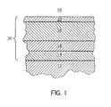
- Integrated circuit 10 generally designates a cross-sectional schematic view of the metallization 30 of an integrated circuit in accordance with an embodiment of the present invention.
- Integrated circuit 10 includes a body or substrate 12 such as a semiconductor body or a Si single crystal substrate.
- underlayer 14 Formed on body 12 is an underlayer 14 of titanium (Ti).
- the thickness of underlayer 14 is preferably in the range of from about 1 nm to about 100 nm and, more preferably, from about 10 nm to about 20 nm. If the underlayer is less than about 1 nm in thickness, it is difficult to ensure that an adequate layer has been deposited. On the other hand, if the underlayer thickness exceeds about 100 nm, then other layers may have to be thinned in order to maintain a predetermined overall thickness of the layered surface and there may be an increased chance of failure of the other layers.
- underlayer 14 should be relatively clean with a controlled degree of contamination. Most preferably, the level of contamination in underlayer 14 should be maintained at or below about 5 wt.%.
- the contaminates can be selected from nitrogen, carbon, and oxygen as well as any other known contaminants that can be substituted for this purpose. Such contaminants can be used alone or in any combination.
- underlayer 14 can be deposited with a collimator to make the deposited material more directional, for example, but it need not be applied with a collimator.
- a TiN layer 16 that is preferably maintained at a thickness at or below about 50 nm. There should at least be a very thin TiN layer in between the TiN and Al layer (to be described) in order to avoid excessive TiAl3 formation. Although not necessary, this TiN layer 16 can be deposited by collimation as well, if desired.
- a deposited layer 18 of AlCu On top of TiN layer 16 as shown in FIG. 1 is a deposited layer 18 of AlCu. It is preferred for the AlCu layer 18 to be within the range from about 20 nm to about 2,000 nm. More preferably, the thickness of the AlCu layer 18 is maintained within the range from about 230 nm to about 370 nm.
- the Al in layer 18 can alternatively be alloyed with a wide variety of solutes such as Cu, Si, and Pd, for example, and multiple solutes can also be used (e.g., AlCuSi) of various components.
- overlayer 20 On AlCu layer 18 is deposited a top overlayer 20 of Ti.
- An overlayer 20 provides a redundant layer for reliability, as an ARC layer, and as an etch layer stop. This overlayer 20 is relatively dirty as compared to Ti underlayer 14 in order to retain an adequate sheet resistance.
- the degree of contamination of overlayer 20 is preferably greater than about 10 wt.% of an impurity or contaminant such as nitrogen, oxygen, carbon, or other such contaminants or combinations of such contaminants.
- the thickness of the overlayer 20 is preferably in the range from about 10 nm to about 100 nm. A more preferred thickness is in the range from about 20 nm to about 50 nm.
- the impurity should be sufficient to reduce the formation of TiAl3 at the juncture between Ti overlayer 20 and AlCu layer 18. At the same time, the degree of contamination should not be so high as to bring about an excessive contact resistance.
- the quality of the underlayer and overlayer in a Complementary Metal-Oxide-Semiconductor (CMOS) wiring stack has been discovered to affect the AlCu texture and sheet resistance as well as the reliability performance.
- the Ti film quality can be improved (i.e., for the underlayer 14) by using any or all of the following: long throw techniques (with an increased distance between the target material and the deposit surface), collimation, ultra high vacuum (UHV) deposition conditions, pasting or Ar clean to remove surface contamination when Ti/TiN deposition is brought about in the same chamber, and high deposition rates.
- the Ti film quality can be decreased (i.e., for the Ti overlayer 20) by using normal throw, only UV deposition conditions, no pasting or Ar clean in the combined Ti/TiN chamber (wherein the nitrogen gas is turned off for Ti deposition and turned on for TiN deposition, both performed in the same chamber), lower deposition rates, or by using a low purity target.
- Various deposition techniques are described in U.S. Patent No. 5,943,601.
- the contamination level is controlled by improving the cleanliness of the background vacuum, by limiting the introduction of impurity gases during metal deposition, and by depositing each of the metal layers in a dedicated chamber to limit the cross-contamination from one metal film to another and improve the purity of each metal film.
- the cleanliness of the Ti underlayer is instrumental in the improvement of electromigration resistance.
- a relatively clean Ti layer can significantly increase the sheet resistance and, at the same time, it can lower electromigration resistance because of increased TiAl3 formation.
- a relatively dirty Ti layer should be used to help resist TiAl3 formation and to achieve a decreased metal sheet resistance while still providing good contact resistance and good adhesion.
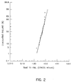
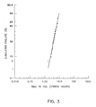
- FIGS. 2 and 3 both illustrate, graphically, the time to failure of samples having a Ti layer that is deposited by collimation techniques (FIG. 3) and non-collimation techniques (FIG. 2).
- the electromigration tests were conducted to compare collimated deposition to non-collimated deposition for clean Ti layers to determine the relative effects of texture and cleanliness on electromigration performance. All of the samples were formed in a dedicated Ti chamber, as opposed to a non-dedicated Ti/TiN chamber, to provide a cleanliness with contaminants comprising less than about 5 wt.% of the Ti layer.
- the samples illustrated in FIG. 2 were prepared in a non-collimated chamber. They were then tested for electromigration at 0.81 mA and 250 ⁇ C.
- the samples illustrated in FIG. 3 were prepared in a collimated chamber. They were also tested for electromigration at 0.81 mA and 250 ⁇ C.
- FIGS. 2 and 3 surprisingly illustrate substantially the same reliability test results as between the collimated samples (FIG. 3) and the non- collimated samples (FIG. 2).
- the results indicate that the cleanliness of the Ti underlayer (brought about by the use of a dedicated Ti chamber in this example) is a significant factor in achieving improved electromigration characteristics and reliability.
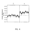
- Ti/TiN/AlCu/Ti/TiN (bottom to top) film stacks were formed to determine the correlation between sheet resistance and the cleanliness of the top Ti layer.
- the structure of each of the film stacks is summarized in the following table: Layer Thickness Top TiN 40 nm Top Ti 5 nm AlCu 230 nm Bottom TiN 10 nm Bottom Ti 10 nm
- FIG. 4 plots the sheet resistance for the case where the top Ti layer has about 5 wt.% or less of a contaminant (primarily nitrogen), shown on side "B" of FIG. 4, and when it has more than about 5 wt.% of a contaminant (primarily nitrogen), shown on side "A” of FIG. 4.
- the sheet resistance is about 5 to 10 wt.% lower when the top Ti layer has increased contamination. This is due at least in part to the prevention of TiAl3 formation between the relatively contaminated top Ti layer and the AlCu conducting layer because of the contamination contained within the Ti layer. Specifically, TiAl3 was formed between the relatively clean Ti top layer and the AlCu layer.
- Ti/TiN/AlCu/Ti/TiN film stacks were formed to determine the correlation between the cleanliness of the bottom Ti layer and electromigration performance.
- the following table shows electromigration results for two film stacks that were similar except that the bottom Ti has about 5 wt.% or less of a contaminant (deposited in a dedicated chamber) in one case and has more than about 5 wt.% of a contaminant (deposited in a shared chamber) in the other case.
- the sample with the relatively clean Ti had a significantly improved electromigration mean time to failure, deviation to mean time to failure, and maximum potential current density as compared to the sample with the relatively dirty Ti. This is characteristic of better electromigration performance for the sample with a Ti bottom layer having reduced contamination.
Landscapes
- Internal Circuitry In Semiconductor Integrated Circuit Devices (AREA)
- Electrodes Of Semiconductors (AREA)
Applications Claiming Priority (2)
| Application Number | Priority Date | Filing Date | Title |
|---|---|---|---|
| US18942898A | 1998-11-10 | 1998-11-10 | |
| US189428 | 1998-11-10 |
Publications (2)
| Publication Number | Publication Date |
|---|---|
| EP1001463A2 true EP1001463A2 (de) | 2000-05-17 |
| EP1001463A3 EP1001463A3 (de) | 2003-05-07 |
Family
ID=22697286
Family Applications (1)
| Application Number | Title | Priority Date | Filing Date |
|---|---|---|---|
| EP99308278A Withdrawn EP1001463A3 (de) | 1998-11-10 | 1999-10-20 | Aluminiumverbindungen mit Unter- und Überlagen aus Titan für integrierte Schaltungen |
Country Status (4)
| Country | Link |
|---|---|
| EP (1) | EP1001463A3 (de) |
| JP (1) | JP2000150520A (de) |
| KR (1) | KR100360740B1 (de) |
| TW (1) | TW457676B (de) |
Cited By (2)
| Publication number | Priority date | Publication date | Assignee | Title |
|---|---|---|---|---|
| EP1458030A3 (de) * | 2003-03-12 | 2006-03-15 | Samsung SDI Co., Ltd. | Neuartige leitende Elemente für Dünnfilmtransistoren in einem Flachbildschirm |
| EP1458029A3 (de) * | 2003-03-12 | 2006-03-15 | Samsung SDI Co., Ltd. | Neuartige leitende Elemente für Dünnfilmtransistoren in einem Flachbildschirm |
Families Citing this family (1)
| Publication number | Priority date | Publication date | Assignee | Title |
|---|---|---|---|---|
| JP2012164940A (ja) * | 2011-02-09 | 2012-08-30 | Rohm Co Ltd | 半導体装置およびその製造方法 |
Family Cites Families (4)
| Publication number | Priority date | Publication date | Assignee | Title |
|---|---|---|---|---|
| JPH0418760A (ja) * | 1989-02-20 | 1992-01-22 | Matsushita Electric Ind Co Ltd | 半導体装置 |
| US5641992A (en) * | 1995-08-10 | 1997-06-24 | Siemens Components, Inc. | Metal interconnect structure for an integrated circuit with improved electromigration reliability |
| US5747879A (en) * | 1995-09-29 | 1998-05-05 | Intel Corporation | Interface between titanium and aluminum-alloy in metal stack for integrated circuit |
| EP0875923A3 (de) * | 1997-04-30 | 1999-11-03 | International Business Machines Corporation | Mehrschichtige Metallisierungsstruktur mit einem IVA-Metall |
-
1999
- 1999-10-14 JP JP11292395A patent/JP2000150520A/ja active Pending
- 1999-10-20 EP EP99308278A patent/EP1001463A3/de not_active Withdrawn
- 1999-10-29 TW TW088118796A patent/TW457676B/zh not_active IP Right Cessation
- 1999-11-03 KR KR1019990048307A patent/KR100360740B1/ko not_active Expired - Fee Related
Cited By (2)
| Publication number | Priority date | Publication date | Assignee | Title |
|---|---|---|---|---|
| EP1458030A3 (de) * | 2003-03-12 | 2006-03-15 | Samsung SDI Co., Ltd. | Neuartige leitende Elemente für Dünnfilmtransistoren in einem Flachbildschirm |
| EP1458029A3 (de) * | 2003-03-12 | 2006-03-15 | Samsung SDI Co., Ltd. | Neuartige leitende Elemente für Dünnfilmtransistoren in einem Flachbildschirm |
Also Published As
| Publication number | Publication date |
|---|---|
| EP1001463A3 (de) | 2003-05-07 |
| TW457676B (en) | 2001-10-01 |
| KR100360740B1 (ko) | 2002-11-13 |
| KR20000035188A (ko) | 2000-06-26 |
| JP2000150520A (ja) | 2000-05-30 |
Similar Documents
| Publication | Publication Date | Title |
|---|---|---|
| EP0843895B1 (de) | Verfahren zur herstellung einer metall-leitungsstruktur für eine integrierte schaltung mit verbessertem elektromigrationswiderstand | |
| KR100301647B1 (ko) | 집적회로,집적회로용 호접속부부 제공방법 및 전도성 스트라이프 | |
| US7247946B2 (en) | On-chip Cu interconnection using 1 to 5 nm thick metal cap | |
| US6255733B1 (en) | Metal-alloy interconnections for integrated circuits | |
| US6174799B1 (en) | Graded compound seed layers for semiconductors | |
| US5700718A (en) | Method for increased metal interconnect reliability in situ formation of titanium aluminide | |
| US6787912B2 (en) | Barrier material for copper structures | |
| EP0716447A2 (de) | Aus geschichteten Subschichten geformte Metallschichten und Anordnungen mit diesen Metallschichten | |
| US20090203208A1 (en) | Copper alloy for wiring, semiconductor device, method for forming wiring, and method for manufacturing semiconductor device | |
| US5278448A (en) | Semiconductor device and method of fabricating the same | |
| US5238874A (en) | Fabrication method for laminated films comprising Al-Si-Co alloy film and refractory metal silioide copper film | |
| US5747879A (en) | Interface between titanium and aluminum-alloy in metal stack for integrated circuit | |
| US7566973B2 (en) | Semiconductor device and method of manufacturing the same | |
| EP1001463A2 (de) | Aluminiumverbindungen mit Unter- und Überlagen aus Titan für integrierte Schaltungen | |
| KR100896159B1 (ko) | 반도체 장치 및 그 제조 방법 | |
| JPH0653216A (ja) | 半導体装置およびその製造方法 | |
| EP0609501B1 (de) | Metallisierung auf Aluminiumbasis für Halbleiterbauelement | |
| CN1266284A (zh) | 上下钛层的洁净度对铝互连可靠性和功能的影响 | |
| JP3347019B2 (ja) | 半導体装置 | |
| US6777810B2 (en) | Interconnection alloy for integrated circuits | |
| WO2004066383A1 (en) | Titanium underlayer for lines in semiconductor devices | |
| HK1028294A (en) | The effects of cleanliness of the titanium under and overlayers on the reliability and functionality of aluminum interconnects | |
| EP0875923A2 (de) | Mehrschichtige Metallisierungsstruktur mit einem IVA-Metall | |
| US20040020891A1 (en) | Low Cu percentages for reducing shorts in AlCu lines | |
| JP2003124211A (ja) | エレクトロマイグレーションを減す構造及び方法 |
Legal Events
| Date | Code | Title | Description |
|---|---|---|---|
| PUAI | Public reference made under article 153(3) epc to a published international application that has entered the european phase |
Free format text: ORIGINAL CODE: 0009012 |
|
| AK | Designated contracting states |
Kind code of ref document: A2 Designated state(s): AT BE CH CY DE DK ES FI FR GB GR IE IT LI LU MC NL PT SE |
|
| AX | Request for extension of the european patent |
Free format text: AL;LT;LV;MK;RO;SI |
|
| PUAL | Search report despatched |
Free format text: ORIGINAL CODE: 0009013 |
|
| AK | Designated contracting states |
Designated state(s): AT BE CH CY DE DK ES FI FR GB GR IE IT LI LU MC NL PT SE |
|
| AX | Request for extension of the european patent |
Extension state: AL LT LV MK RO SI |
|
| 17P | Request for examination filed |
Effective date: 20030522 |
|
| AKX | Designation fees paid |
Designated state(s): AT BE CH CY DE DK ES FI FR GB GR IE IT LI LU MC NL PT SE |
|
| STAA | Information on the status of an ep patent application or granted ep patent |
Free format text: STATUS: THE APPLICATION HAS BEEN WITHDRAWN |
|
| 18W | Application withdrawn |
Effective date: 20051227 |