EP1001475A2 - Procédé de fabrication d'un dispositif organique électroluminescent - Google Patents
Procédé de fabrication d'un dispositif organique électroluminescent Download PDFInfo
- Publication number
- EP1001475A2 EP1001475A2 EP99203588A EP99203588A EP1001475A2 EP 1001475 A2 EP1001475 A2 EP 1001475A2 EP 99203588 A EP99203588 A EP 99203588A EP 99203588 A EP99203588 A EP 99203588A EP 1001475 A2 EP1001475 A2 EP 1001475A2
- Authority
- EP
- European Patent Office
- Prior art keywords
- light
- layer
- dopant
- emitting
- organic
- Prior art date
- Legal status (The legal status is an assumption and is not a legal conclusion. Google has not performed a legal analysis and makes no representation as to the accuracy of the status listed.)
- Withdrawn
Links
Images




Classifications
-
- H—ELECTRICITY
- H10—SEMICONDUCTOR DEVICES; ELECTRIC SOLID-STATE DEVICES NOT OTHERWISE PROVIDED FOR
- H10K—ORGANIC ELECTRIC SOLID-STATE DEVICES
- H10K50/00—Organic light-emitting devices
- H10K50/10—OLEDs or polymer light-emitting diodes [PLED]
- H10K50/11—OLEDs or polymer light-emitting diodes [PLED] characterised by the electroluminescent [EL] layers
-
- H—ELECTRICITY
- H10—SEMICONDUCTOR DEVICES; ELECTRIC SOLID-STATE DEVICES NOT OTHERWISE PROVIDED FOR
- H10K—ORGANIC ELECTRIC SOLID-STATE DEVICES
- H10K71/00—Manufacture or treatment specially adapted for the organic devices covered by this subclass
- H10K71/30—Doping active layers, e.g. electron transporting layers
Definitions
- the present invention relates to methods of making organic light-emitting devices and, more particularly to methods of providing in a light-emitting layer of an organic light-emitting device a dopant capable of modifying light emitted from the device.
- Organic light-emitting devices also referred to as organic electroluminescent (EL) devices or as organic internal junction light-emitting devices, contain spaced electrodes separated by an organic light-emitting structure (also referred to as an organic EL medium) which emits light in response to the application of an electrical potential difference across the electrodes.
- At least one of the electrodes is light-transmissive, and the organic light-emitting structure can have a multi-layer of organic thin films which provide for hole injection and transport from an anode, and for electron injection and transport from a cathode, respectively, with light emission resulting from electron-hole recombination at an internal junction formed at an interface between the hole-transporting and the electron-transporting thin films.
- the term "thin film” refers to layer thicknesses of less than 1 micrometer with layer thickness of less than about 0.5 micrometer being typical.
- Examples of organic light-emitting devices containing organic light-emitting structures and cathode constructions formed by thin film deposition techniques are provided in US-A-4,356,429; US-A-4,539,507 and US-A-4,720,432; and US-A-4,769,292.
- the spectral distribution of emitted light is related to the electroluminescent properties of the organic thin films used in the device construction. For example, if an organic light-emitting structure includes a layer which contains a light-emitting host material, the emitted light will be dominated by the light emission from the host material.
- the organic thin films of a light-emitting device are formed by vapor deposition (evaporation or sublimation) in successive deposition steps within a vacuum system which employs a deposition rate control.
- a fluorescent dopant is to be uniformly incorporated within an organic light-emitting layer
- the light-emitting host material and the fluorescent dopant material are co-deposited from two independently controlled deposition sources. It has been found to be difficult to reliably control the deposition rate of a fluorescent dopant when a desired dopant concentration in the host material of the organic light-emitting layer is at or near a lower end of a dopant concentration range of 10 -3 to about 10 mole percent.
- the difficulty of reliably controlling the deposition rates of an organic light-emitting host material and of a fluorescent dopant material has been an obstacle in the process of reproducibly fabricating organic electroluminescent devices containing a fluorescent dopant or fluorescent dopants.
- the present invention has as its purpose to separate the deposition of the organic host material forming the light-emitting layer from the deposition of an organic dopant material, and to introduce the dopant material into the host material during a subsequent processing step.
- an object of the present invention to provide a method of making an organic light-emitting device by forming a light-emitting layer of a light-emitting host material, forming at least one organic dopant layer adjacent to the light-emitting layer, and diffusing the dopant from the dopant layer into the light-emitting layer.
- this object is achieved by the steps of:
- this object is achieved by forming a first organic light-emitting layer, forming at least one organic dopant layer over the first light-emitting layer, forming a second organic light-emitting layer over the dopant layer, and diffusing the dopant from the dopant layer into the first and second light-emitting layers.
- this object is achieved by first forming at least one organic dopant layer, forming an organic light-emitting layer over the dopant layer, and diffusing the dopant from the dopant layer into the light-emitting layer.
- each of these layers can be formed separately to a desired thickness, thereby obviating the problems of deposition rate control associated with the prior art method of forming a doped light-emitting layer.
- the deposition processes are greatly simplified and require equipment of reduced complexity.
- the light-emitting layer of the organic light-emitting host material can be formed by conventional vapor deposition (evaporation, sublimation) and, alternatively, by solution coating of a polymeric organic light-emitting host material.
- the dopant layer can be formed by conventional vapor deposition and, alternatively, by thermally induced transfer from a dopant donor layer formed on a donor support.
- Two or more dopant layers containing different dopants can be formed adjacent to a light-emitting layer, thereby providing a broader range of options for modifying the light emitted from the light-emitting layer.
- Diffusion of a dopant or of dopants from a dopant layer or from dopant layers into an organic light-emitting layer by a fluid vapor treatment process requires relatively simple equipment and provides for relatively rapid processing to achieve uniform dispersion of the dopant or dopants throughout the organic light-emitting layer of the host material.
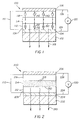
- an organic light-emitting device 100 shows, in sequence, a light-transmissive substrate 102, a light-transmissive anode 104, an organic light-emitting structure 110 formed over the anode, and a cathode 106 provided over the light-emitting structure.
- the organic light-emitting structure 110 comprises, in sequence, a hole-transporting layer 112, a light-emitting layer 114, and an electron-transporting layer 118.
- a junction 150 is formed at an interface between the hole-transporting layer 112 and the light-emitting layer 114 which is also capable of transporting electrons.
- the anode and cathode are connected to an external power source (drive voltage supply) by leads 124 and 126, respectively.
- the source 120 can be a continuous direct current or alternating current voltage source or an intermittent current voltage source. Any convenient conventional power source, including any desired switching circuitry, can be employed which is capable of positively biasing the anode with respect to the cathode. Either the anode or cathode can be at ground potential.
- the internal junction organic light-emitting device can be viewed as a diode which is forward biased when the anode is at a more positive potential than the cathode. Under these conditions, injection of holes 130 occurs from the anode 104 into the hole-transporting layer 112 as schematically shown by arrows 132, while electrons 140 are injected from the cathode 106 into the electron-transporting layer 118 as schematically shown by arrows 142. The injected holes and electrons each migrate toward the oppositely charged electrode, and hole-electron recombination occurs at or near the junction 150. When a migrating electron drops from its conduction band potential to a valance band in filling a hole, energy is released as light.
- the released light can be emitted from the light-emitting structure 110 through one or more side surfaces 108 or, as is usually preferred, the light is emitted through the light-transmissive anode 104 and the light-transmissive substrate 102 as indicated by the straight arrows 165.
- This emitted light substantially corresponds to light-emitting properties of a light-emitting organic host material of which the light-emitting layer 114 is constructed.
- the organic light-emitting device 200 differs from the device of FIG. 1 in that the light-emitting layer 214 contains a dopant 215 selected to modify the host light emission of the host material, as schematically indicated by wavy arrows 265.
- FIGS. 3A-3D there is shown a sequence of process steps which, taken together, illustrate one method of making an organic light-emitting device in accordance with the present invention.
- a light-transmissive anode 304 is provided over a light-transmissive substrate 302. Formed over the anode is an organic hole-transporting layer 312, and an organic light-emitting layer 314 is formed over the hole-transporting layer.
- a junction 350 is indicated at an interface between the hole-transporting layer 312 and the light-emitting layer 314 which is also capable of transporting electrons therethrough.
- the light-transmissive substrate 302 is electrically insulative and can be selected from glass, quartz, and plastic materials.
- the anode 304 is preferably formed of an anode material selected to provide hole injection from the anode into the hole-transporting layer 312. Suitable anode materials include indium oxide, tin oxide, and indium tin oxide (ITO).
- the hole-transporting layer 312 is preferably formed over the anode by vapor depositing an organic hole-transporting material. Following the teachings of US-A-4,539,507, the hole-transporting material is preferably selected from the group consisting of aromatic tertiary amines.
- the organic light-emitting layer 314 can be formed by vapor depositing an organic light-emitting host material to a desired thickness.
- Particularly preferred host materials for forming the light-emitting layer 314 are metal chelated oxinoid compounds, as disclosed in US-A-4,769,292 cited above.
- Particularly preferred metal chelated oxinoid compounds are mixed ligand aluminum chelates as the type disclosed in US-A-5,150,006.
- the light-emitting layer 314 can be formed by solution coating of a polymeric organic light-emitting host material.
- polymeric light-emitting host materials suitable for solution coating include polyphenylene vinylenes (PPV), PPV copolymers, polyanilines, poly-3-alkylthiopenes, poly-3-octylthiopenes, and polyparaphenylenes, following the teachings disclosed in US-A-5,807,627 the disclosure of which is incorporated herein by reference.
- a dopant layer 313 is formed over the light-emitting layer 314.
- the dopant layer contains a fluorescent dopant 315, shown in dotted outline, which, when diffused into the underlying light-emitting layer, will modify the light emitted from the host material.
- the dopant layer 313 can be formed by conventional vacuum vapor deposition of a fluorescent dye functioning as a dopant in a light-emitting host material.
- the dopant layer can be formed by thermal transfer of a dopant donor layer disposed on a donor support, as will be discussed in greater detail with reference to FIGS. 7A-7C.
- particularly preferred dopants are fluorescent dyes which are capable of emitting light in response to hole-electron recombination at or near the junction 350, thereby modifying the light emitted from the host material.
- fluorescent dyes are those selected from the dye classes consisting of coumarin, dicyanomethylenepyrans and thiopyrans, polymethine, oxabenzanthracene, xanthene, pyrylium and thiapyrylium, carbostyril, and perylene fluorescent dyes.
- FIG. 3C there is schematically depicted a dopant layer diffusion step in which the dopant layer 313 of FIG. 3B and the light-emitting layer 314 are exposed to vapor of a fluid or of a fluid mixture selected to provide molecular diffusion paths in the light-emitting layer so as to permit uniform diffusion of the dopant 315 throughout the host material of the light-emitting layer 314.
- the fluid vapor 910 is schematically indicated by dashed arrows, and the fluid vapor treatment process and system will be described in more detail with reference to FIGS. 8A and 8B. As depicted in FIG.
- the dopant material 315 is now uniformly dispersed throughout the light-emitting host material of the layer 314, and no residue of the dopant in the dopant layer 313 of FIG. 3B remains on the surface of the layer 314 after the diffusion step.
- all of the dopant 315 in the dopant layer 313 of FIG. 3B can be diffused into the light-emitting layer during a diffusion time ranging from a few seconds to about 30 seconds.
- FIG. 3D there is shown a completed organic light-emitting device 300, in which an electron-transporting layer 318 is formed over the now doped light-emitting layer 314, and a cathode 306 is shown disposed over the electron-transporting layer.
- the electron-transporting layer 318 is preferably formed by vapor depositing an organic electron-transporting material which is also preferably a metal chelated oxinoid compound.
- the cathode 306 can be vapor deposited, and of a cathode material selected to provide electron injection from the cathode into the electron-transporting layer 318.
- particularly preferred cathode materials are composite materials comprised of a low work function metal (a work function smaller than 4.0 eV) and a second metal which preferably has a work function greater than 4.0 eV, which includes metals more resistant to oxidation and which are therefore more commonly fabricated as metallic layers.
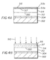
- FIGS. 4A and 4B there is shown another aspect of the present invention, in that a method is provided of forming a first dopant layer 313a containing a dopant material 317 over the light-emitting layer 314, and forming a second dopant layer 313b which contains a dopant material 315 over the first dopant layer.
- FIG. 4B the dopants 317 and 315 are shown uniformly diffused throughout the light-emitting layer 314 by action of the fluid vapor 910 in a manner as previously described.
- a dopant layer 413 containing a dopant material 415, is formed over a hole-transporting layer 412 by either a method of vacuum vapor deposition or by a method of thermal transfer of a dopant donor layer disposed on a donor support.
- a light-emitting layer 414 of a light-emitting host material is formed over the dopant layer 413, as shown in FIG. 5B.
- fluid vapor 920 creates molecular diffusion paths in the light-emitting layer 414 and promotes diffusion of the dopant 415 in the dopant layer 413 into the light-emitting layer. While it may appear from the drawings of FIGS. 5B and 5C that the doped light-emitting layer 414 could be lifted off the hole-transporting layer 412 when the dopant layer 413 in FIG. 5B substantially vanishes as the dopant 415 diffuses upwardly into the light-emitting layer 414, it will be appreciated that the dopant layer 413 is formed to a thickness in a range of .1-1 nm (1-10 Angstrom), that is to a thickness of molecular dimensions.
- FIG. 5D depicts a completed organic light-emitting device 400 constructed in accordance with the methods of the present invention.
- a first light-emitting layer 514a is formed over a hole-transporting layer 512.
- a dopant layer 513 containing a dopant material 515 is formed over the first light-emitting layer.
- a second light-emitting layer 514b is formed over the dopant layer 513.
- the thin (.1-1.0 nm) dopant layer 513 is sandwiched between two undoped light-emitting layers which may comprise two different light-emitting host materials.
- a fluid vapor 930 has uniformly diffused the dopant material 515 from the dopant layer 513 of FIG. 6B to form a doped light-emitting layer 514, which is shown here as containing the dopant in a single light-emitting host material.
- FIG. 6D depicts a completed organic light-emitting device 500 constructed by a method in accordance with the present invention.
- a dopant donor assembly 600 has a donor support 622, and a dopant donor layer 633 formed on one surface of the support, and containing a dopant 635.
- the dopant donor layer 633 can be formed by conventional vacuum vapor deposition methods to a desired thickness, and of one of the preferred fluorescent dye dopant materials discussed previously.
- the dopant donor assembly 600 is shown positioned in close proximity to, and substantially parallel with, an upper surface of a light-emitting layer 714 which is to receive a dopant layer by thermally induced transfer of the dopant 635 in the dopant donor layer 633.
- the donor support is heated by radiation 680.
- a diminishing or diminished dopant donor layer 633a is indicated, as well as a growing dopant donor layer 713a being formed into a completely transferred dopant layer 713 shown in FIG. 7C.
- the dopant 715 in the dopant layer 713 can now be diffused into the light-emitting layer 714 in a manner identical to the previously discussed dopant diffusing step.
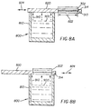
- a vapor treatment system 800 is schematically indicated comprising a container 810 which contains a vaporizable fluid to a level 900, the fluid producing a fluid vapor 910, shown by dashed arrows, in a volume extending between a sealed sliding cover 820 and the fluid level 900.
- the sliding cover has a recessed aperture 822 into which can be positioned a device in preparation for diffusion of a dopant from a dopant layer into a light-emitting layer.
- a device having a light-emitting layer 314 and an overlying dopant layer 313.
- the sliding cover has been translated by a sliding motion as indicated at 824, so as to expose the dopant layer and the light-emitting layer to the fluid vapor 910 for a defined period of time, and to thereby diffuse the dopant material from the dopant layer 313 into the light-emitting layer 314.
- a vapor treatment system can be readily constructed to control vapor formation within the container 810 by heating and/or cooling means (not shown) surrounding the interior or exterior of the container.
- fluids and fluid mixtures can be selected to provide fluid vapors useful for diffusing a dopant from a dopant layer into a light-emitting layer at or near room temperature.
- fluids and fluid mixtures can be selected from among alcohols such as isopropanol; ketones, such as acetone and 2-butanone; and chlorinated fluids, such as dichloromethane.
- a device designated for measurement of photoluminescence, was constructed as follows:
- Example 2 A device was constructed in the manner of Example 1, but with an additional dopant diffusion step in isopropanol vapor for 8 seconds. This device is abbreviated as:
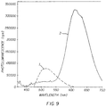
- the spectral distribution of the photoluminescence (fluorescence) of both devices was measured in a spectrofluorometer, Fluoro Max-2 manufactured by Instruments S.A., Inc., at a fixed excitation wavelength of 390 nm.
- the relative fluorescence intensity is measured as counts per second (cps).
- FIG. 9 shows that device 1 (Example 1; dashed trace) has a fluorescence emission peak in a blue-green spectral region centered at about 515 nm, characteristic of the photoluminescence of undoped Alq host material.
- Device 2 (Example 2; solid trace) exhibits a significantly red-shifted emission with a peak emission at about 610 nm, and having a significantly higher photoluminescence peak intensity.
- diffusing the DCJTB dopant from the 2.1 nm dopant layer into the first and second Alq light-emitting layers has resulted in significant modification of the photoluminescence of the Alq host layer.
- An organic light-emitting device was constructed in the following manner:
- This device is abbreviated as:
- An organic light-emitting device was made in the following manner:
- This device is abbreviated as:
- the devices of Examples 3 and 4 were operated by applying a drive voltage between respective anode and cathode electrodes, with the anodes biased positively.
- the drive voltage was adjusted so that each device operated at a current density of 20 mA/cm 2 .
- the spectral radiance of the emitted light was measured with equipment available from Photo Research Laboratory (Model (PR650)).
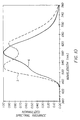
- FIG. 10 depicts the normalized electroluminescent spectral radiance traces of device 3 (Example 3; dashed trace) and of device 4 (Example 4; solid trace). It is apparent that device 4 exhibits a spectral radiance resembling the characteristics of the dopant DCJTB having a radiance peak at 580 nm. Device 3 exhibits a spectral radiance resembling the characteristics of a combination of host Alq and dopant DCJTB with a first peak at about 520 nm and a second peak at about 620 nm. The luminous efficiency, given in lumen/Watt, was 0.42 for device 3, and 1.16 for device 4, indicating that the device with diffused dopants in the emitting layer is substantially higher than the undiffused device.
- An organic light-emitting device was made in the following manner:
- This device is abbreviated as:
- the device is abbreviated as:
- the devices of Examples 5 and 6 were operated by applying a drive voltage between respective anode and cathode electrodes, with the anodes biased positively.
- the drive voltage was adjusted so that each device operated at a current density of 20 mA/cm 2 .
- the spectral radiance of the emitted light was measured with equipment available from Photo Research Laboratory (Model (PR650)).
- FIG. 11 depicts the normalized electroluminescent spectral radiance traces of device 5 (Example 5; dashed trace) and of device 6 (Example 6; solid trace). It is apparent that device 6 exhibits a spectral radiance resembling the characteristics of the dopant DCJTB having a radiance peak at 585 nm. Device 5 exhibits a spectral radiance resembling the characteristics of a combination of host Alq and dopant DCJTB with a first peak at about 530 nm and a second peak at about 625 nm. The luminous efficiency, given in lumen/Watt, was 0.25 for device 5, and 1.28 for device 6, indicating that the device with diffused dopants in the emitting layer is substantially higher than the undiffused device.
- the method of making an organic light-emitting device wherein the dopant layer providing step includes vapor depositing a fluorescent dye over a surface of the support.
- the method of making an organic light-emitting device wherein the fluorescent dye vapor depositing step includes vapor depositing a fluorescent dye selected from the class consisting of coumarin, dicyanomethylenepyrans and thiopyrans, polymethine, oxabenzanthracene, xanthene, pyrylium and thiapyrylium, carbostyril, and perylene fluorescent dyes.
- a fluorescent dye selected from the class consisting of coumarin, dicyanomethylenepyrans and thiopyrans, polymethine, oxabenzanthracene, xanthene, pyrylium and thiapyrylium, carbostyril, and perylene fluorescent dyes.
- the method of making an organic light-emitting device wherein the dopant diffusing step includes exposing the dopant layer and the light-emitting layer to vapor of a fluid or of a fluid mixture selected to provide molecular diffusion paths in the light-emitting layer which permit uniform diffusion of the dopant throughout the host material of the light-emitting layer.
- the method of making an organic light-emitting device wherein the electron-transporting layer forming step includes vapor depositing an organic electron-transporting material selected from the group consisting of metal chelated oxinoid compounds.
- the method of making an organic light-emitting device wherein the cathode disposing step includes vapor depositing a cathode and of a cathode material selected to provide electron injection from the cathode into the electron-transporting layer.
- the method of making an organic light-emitting device wherein the substrate providing step includes providing a light-transmissive and electrically insulative substrate.
- the method of making an organic light-emitting device wherein the anode disposing step includes disposing a light-transmissive anode over the substrate and of an anode material selected to provide hole injection from the anode into the hole-transporting layer.
- the method of making an organic light-emitting device wherein the hole-transporting layer forming step includes vapor depositing an organic hole-transporting material selected from the group consisting of aromatic tertiary amines.
- the method of making an organic light-emitting device wherein the steps of forming the first and second light-emitting layers includes vapor depositing an organic light-emitting host material selected from the group consisting of metal chelated oxinoid compounds.
- the method of making an organic light-emitting device wherein the step of forming the first light-emitting layer includes solution coating a polymeric organic light-emitting host material selected from the group consisting of polyparaphenylene vinylene (PPV), PPV copolymers, polyanilines, poly-3-alkylthiopenes, poly-3-octylthiopenes, and polyparaphenylenes.
- PPV polyparaphenylene vinylene
- PPV copolymers polyanilines
- poly-3-alkylthiopenes poly-3-octylthiopenes
- polyparaphenylenes polyparaphenylenes
- the method of making an organic light-emitting device wherein the dopant layer forming step includes vapor depositing a fluorescent dye.
- the method of making an organic light-emitting device wherein the fluorescent dye vapor depositing step includes vapor depositing a fluorescent dye selected from the class consisting of coumarin, dicyanomethylenepyrans and thiopyrans, polymethine, oxabenzanthracene, xanthene, pyrylium and thiapyrylium, carbostyril, and perylene fluorescent dyes.
- a fluorescent dye selected from the class consisting of coumarin, dicyanomethylenepyrans and thiopyrans, polymethine, oxabenzanthracene, xanthene, pyrylium and thiapyrylium, carbostyril, and perylene fluorescent dyes.
- the method of making an organic light-emitting device wherein the dopant layer forming step includes the steps of:
- the method of making an organic light-emitting device wherein the dopant layer providing step includes vapor depositing a fluorescent dye over a surface of the support.
- the method of making an organic light-emitting device wherein the fluorescent dye vapor depositing step includes vapor depositing a fluorescent dye selected from the class consisting of coumarin, dicyanomethylenepyrans and thiopyrans, polymethine, oxabenzanthracene, xanthene, pyrylium and thiapyrylium, carbostyril, and perylene fluorescent dyes.
- a fluorescent dye selected from the class consisting of coumarin, dicyanomethylenepyrans and thiopyrans, polymethine, oxabenzanthracene, xanthene, pyrylium and thiapyrylium, carbostyril, and perylene fluorescent dyes.
- the method of making an organic light-emitting device wherein the dopant diffusing step includes exposing the second light-emitting layer, the dopant layer, and the first light-emitting layer to vapor of a fluid or of a fluid mixture selected to provide molecular diffusion paths in the second and first light-emitting layers which permit uniform diffusion of the dopant throughout the host material of the second and first light-emitting layers.
- the method of making an organic light-emitting device wherein the electron-transporting layer forming step includes vapor depositing an organic electron-transporting material selected from the group consisting of metal chelated oxinoid compounds.
- the method of making an organic light-emitting device wherein the cathode disposing step includes vapor depositing a cathode and of a cathode material selected to provide electron injection from the cathode into the electron-transporting layer.
- a method of making an organic light-emitting device comprising the steps of:
- the method of making an organic light-emitting device wherein the substrate providing step includes providing a light-transmissive and electrically insulative substrate.
- the method of making an organic light-emitting device wherein the anode disposing step includes disposing a light-transmissive anode over the substrate and of an anode material selected to provide hole injection from the anode into the hole-transporting layer.
- the method of making an organic light-emitting device wherein the hole-transporting layer forming step includes vapor depositing an organic hole-transporting material selected from the group consisting of aromatic tertiary amines.
- the method of making an organic light-emitting device wherein the dopant layer forming step includes vapor depositing a fluorescent dye.
- the method of making an organic light-emitting device wherein the fluorescent dye vapor depositing step includes vapor depositing a fluorescent dye selected from the class consisting of coumarin, dicyanomethylenepyrans and thiopyrans, polymethine, oxabenzanthracene, xanthene, pyrylium and thiapyrylium, carbostyril, and perylene fluorescent dyes.
- a fluorescent dye selected from the class consisting of coumarin, dicyanomethylenepyrans and thiopyrans, polymethine, oxabenzanthracene, xanthene, pyrylium and thiapyrylium, carbostyril, and perylene fluorescent dyes.
- the method of making an organic light-emitting device wherein the dopant layer forming step includes the steps of:
- the method of making an organic light-emitting device wherein the dopant layer providing step includes vapor depositing a fluorescent dye over a surface of the support.
- the method of making an organic light-emitting device wherein the fluorescent dye vapor depositing step includes vapor depositing a fluorescent dye selected from the class consisting of coumarin, dicyanomethylenepyrans and thiopyrans, polymethine, oxabenzanthracene, xanthene, pyrylium and thiapyryliurn, carbostyril, and perylene fluorescent dyes.
- a fluorescent dye selected from the class consisting of coumarin, dicyanomethylenepyrans and thiopyrans, polymethine, oxabenzanthracene, xanthene, pyrylium and thiapyryliurn, carbostyril, and perylene fluorescent dyes.
- the method of making an organic light-emitting device wherein the dopant diffusing step includes exposing the dopant layer and the light-emitting layer to vapor of a fluid or of a fluid mixture selected to provide molecular diffusion paths in the light-emitting layer which permit uniform diffusion of the dopant throughout the host material of the light-emitting layer.
- the method of making an organic light-emitting device wherein the electron-transporting layer forming step includes vapor depositing an organic electron-transporting material selected from the group consisting of metal chelated oxinoid compounds.
- the method of making an organic light-emitting device wherein the cathode disposing step includes vapor depositing a cathode and of a cathode material selected to provide electron injection from the cathode into the electron-transporting layer.
- the method of making an organic light-emitting device wherein the dopant layer forming step includes the steps of:
- the method of making an organic light-emitting device wherein the dopant diffusing step includes exposing the first and second dopant layers and the light-emitting layer to vapor of a fluid or of a fluid mixture selected to provide molecular diffusion paths in the light-emitting layer which permit uniform diffusion of the dopants throughout the host material of the light-emitting layer.
Landscapes
- Physics & Mathematics (AREA)
- Optics & Photonics (AREA)
- Electroluminescent Light Sources (AREA)
Applications Claiming Priority (2)
| Application Number | Priority Date | Filing Date | Title |
|---|---|---|---|
| US192066 | 1980-09-29 | ||
| US09/192,066 US6048573A (en) | 1998-11-13 | 1998-11-13 | Method of making an organic light-emitting device |
Publications (2)
| Publication Number | Publication Date |
|---|---|
| EP1001475A2 true EP1001475A2 (fr) | 2000-05-17 |
| EP1001475A3 EP1001475A3 (fr) | 2004-01-14 |
Family
ID=22708090
Family Applications (1)
| Application Number | Title | Priority Date | Filing Date |
|---|---|---|---|
| EP99203588A Withdrawn EP1001475A3 (fr) | 1998-11-13 | 1999-11-01 | Procédé de fabrication d'un dispositif organique électroluminescent |
Country Status (3)
| Country | Link |
|---|---|
| US (1) | US6048573A (fr) |
| EP (1) | EP1001475A3 (fr) |
| JP (1) | JP2000150151A (fr) |
Families Citing this family (46)
| Publication number | Priority date | Publication date | Assignee | Title |
|---|---|---|---|---|
| GB2347013A (en) * | 1999-02-16 | 2000-08-23 | Sharp Kk | Charge-transport structures |
| US6821643B1 (en) * | 2000-01-21 | 2004-11-23 | Xerox Corporation | Electroluminescent (EL) devices |
| US6392250B1 (en) * | 2000-06-30 | 2002-05-21 | Xerox Corporation | Organic light emitting devices having improved performance |
| US7588795B2 (en) * | 2000-08-24 | 2009-09-15 | Samsung Mobile Display Co., Ltd. | Manufacturing method of OLED display and apparatus for manufacturing the OLED display |
| KR100342653B1 (ko) * | 2000-08-24 | 2002-07-03 | 김순택 | 유기 전계발광소자의 제조 방법 |
| TW518909B (en) * | 2001-01-17 | 2003-01-21 | Semiconductor Energy Lab | Luminescent device and method of manufacturing same |
| US20020110673A1 (en) | 2001-02-14 | 2002-08-15 | Ramin Heydarpour | Multilayered electrode/substrate structures and display devices incorporating the same |
| SG118118A1 (en) * | 2001-02-22 | 2006-01-27 | Semiconductor Energy Lab | Organic light emitting device and display using the same |
| EP1289015B1 (fr) * | 2001-08-28 | 2012-05-23 | Konica Corporation | Dispositif émetteur de lumière en plusieurs couleurs et procédé de production de ce dispositif |
| US7488986B2 (en) * | 2001-10-26 | 2009-02-10 | Semiconductor Energy Laboratory Co., Ltd. | Light emitting device |
| JP4498669B2 (ja) | 2001-10-30 | 2010-07-07 | 株式会社半導体エネルギー研究所 | 半導体装置、表示装置、及びそれらを具備する電子機器 |
| US6579237B1 (en) | 2001-12-14 | 2003-06-17 | Koninklijke Philips Electronics Nv | Diagnostic ultrasonic imaging system having organic light emitting device display |
| WO2003076548A1 (fr) | 2002-03-09 | 2003-09-18 | Cdt Oxford Limited | Compositions polymerisables et dispositifs electroluminescents organiques les contenant |
| US6811815B2 (en) * | 2002-06-14 | 2004-11-02 | Avery Dennison Corporation | Method for roll-to-roll deposition of optically transparent and high conductivity metallic thin films |
| US6939660B2 (en) * | 2002-08-02 | 2005-09-06 | Eastman Kodak Company | Laser thermal transfer donor including a separate dopant layer |
| US7098060B2 (en) * | 2002-09-06 | 2006-08-29 | E.I. Du Pont De Nemours And Company | Methods for producing full-color organic electroluminescent devices |
| KR100650046B1 (ko) * | 2002-11-20 | 2006-11-27 | 엘지전자 주식회사 | 고효율의 유기 전계 발광 소자 |
| US20040140758A1 (en) * | 2003-01-17 | 2004-07-22 | Eastman Kodak Company | Organic light emitting device (OLED) display with improved light emission using a metallic anode |
| US6841270B2 (en) | 2003-04-17 | 2005-01-11 | Canon Kabushiki Kaisha | Organic light-emitting device having pyrylium salt as charge transport material |
| CN1839174A (zh) * | 2003-08-20 | 2006-09-27 | 陶氏康宁公司 | 咔唑基官能聚硅氧烷树脂,硅氧烷组合物,和有机发光二极管 |
| EP1660564A1 (fr) * | 2003-08-20 | 2006-05-31 | Dow Corning Corporation | Polysiloxanes lin aires fonctionnalit carbazolyle, composition de silicone et diode lectroluminescente organique |
| KR20060120588A (ko) * | 2003-08-20 | 2006-11-27 | 다우 코닝 코포레이션 | 카바졸릴 작용성 사이클로실록산, 실리콘 조성물 및 유기발광 다이오드 |
| US20050100657A1 (en) * | 2003-11-10 | 2005-05-12 | Macpherson Charles D. | Organic material with a region including a guest material and organic electronic devices incorporating the same |
| EP1735850A1 (fr) * | 2004-03-16 | 2006-12-27 | Dow Corning Corporation | Matiere de transport de trous comprenant des polysiloxanes |
| EP1730798A1 (fr) * | 2004-03-16 | 2006-12-13 | Dow Corning Corporation | Diode electroluminescente organique |
| US7067841B2 (en) * | 2004-04-22 | 2006-06-27 | E. I. Du Pont De Nemours And Company | Organic electronic devices |
| US20080007158A1 (en) * | 2004-06-15 | 2008-01-10 | Omar Farooq | Linear Polysiloxanes, Silicone Composition, and Organic Light-Emitting Diode |
| US7515149B2 (en) * | 2004-12-17 | 2009-04-07 | Eastman Kodak Company | Display with wirelessly controlled illumination |
| US20060131505A1 (en) * | 2004-12-17 | 2006-06-22 | Eastman Kodak Company | Imaging element |
| US7538756B2 (en) * | 2004-12-17 | 2009-05-26 | Eastman Kodak Company | Methods for making display |
| US20060136734A1 (en) * | 2004-12-21 | 2006-06-22 | Eastman Kodak Company | Identification display device |
| US20060136997A1 (en) * | 2004-12-21 | 2006-06-22 | Eastman Kodak Company | Authentication system and method |
| US20060131393A1 (en) * | 2004-12-22 | 2006-06-22 | Eastman Kodak Company | Multi-role transaction card |
| US7268006B2 (en) * | 2004-12-30 | 2007-09-11 | E.I. Du Pont De Nemours And Company | Electronic device including a guest material within a layer and a process for forming the same |
| US7630029B2 (en) * | 2005-02-16 | 2009-12-08 | Industrial Technology Research Institute | Conductive absorption layer for flexible displays |
| US20070001927A1 (en) * | 2005-07-01 | 2007-01-04 | Eastman Kodak Company | Tiled display for electronic signage |
| US20070096640A1 (en) * | 2005-08-19 | 2007-05-03 | Gang Yu | Methods for producing full color organic electroluminescent devices |
| US20070085838A1 (en) | 2005-10-17 | 2007-04-19 | Ricks Theodore K | Method for making a display with integrated touchscreen |
| US20070085837A1 (en) * | 2005-10-17 | 2007-04-19 | Eastman Kodak Company | Touch input device with display front |
| US7601567B2 (en) * | 2005-12-13 | 2009-10-13 | Samsung Mobile Display Co., Ltd. | Method of preparing organic thin film transistor, organic thin film transistor, and organic light-emitting display device including the organic thin film transistor |
| US20080166566A1 (en) * | 2006-12-29 | 2008-07-10 | Shiva Prakash | Process for forming an organic light-emitting diode and devices made by the process |
| CN102015900B (zh) * | 2008-03-26 | 2012-11-07 | 陶氏康宁公司 | 硅氧烷组合物和有机发光二极管 |
| US8878589B2 (en) | 2011-06-30 | 2014-11-04 | Semiconductor Energy Laboratory Co., Ltd. | Semiconductor device and driving method thereof |
| US10043794B2 (en) | 2012-03-22 | 2018-08-07 | Semiconductor Energy Laboratory Co., Ltd. | Semiconductor device and electronic device |
| US10483293B2 (en) | 2014-02-27 | 2019-11-19 | Semiconductor Energy Laboratory Co., Ltd. | Active matrix display device, and module and electronic appliance including the same |
| JP2018032018A (ja) | 2016-08-17 | 2018-03-01 | 株式会社半導体エネルギー研究所 | 半導体装置、表示モジュール及び電子機器 |
Family Cites Families (7)
| Publication number | Priority date | Publication date | Assignee | Title |
|---|---|---|---|---|
| US4356429A (en) * | 1980-07-17 | 1982-10-26 | Eastman Kodak Company | Organic electroluminescent cell |
| US4539507A (en) * | 1983-03-25 | 1985-09-03 | Eastman Kodak Company | Organic electroluminescent devices having improved power conversion efficiencies |
| US4720432A (en) * | 1987-02-11 | 1988-01-19 | Eastman Kodak Company | Electroluminescent device with organic luminescent medium |
| US4769292A (en) * | 1987-03-02 | 1988-09-06 | Eastman Kodak Company | Electroluminescent device with modified thin film luminescent zone |
| US5194290A (en) * | 1987-12-31 | 1993-03-16 | The United States Of America As Represented By The Administrator Of The National Aeronautics And Space Administration | Method of making a single layer multi-color luminescent display |
| US5150006A (en) * | 1991-08-01 | 1992-09-22 | Eastman Kodak Company | Blue emitting internal junction organic electroluminescent device (II) |
| US5688551A (en) * | 1995-11-13 | 1997-11-18 | Eastman Kodak Company | Method of forming an organic electroluminescent display panel |
-
1998
- 1998-11-13 US US09/192,066 patent/US6048573A/en not_active Expired - Lifetime
-
1999
- 1999-11-01 EP EP99203588A patent/EP1001475A3/fr not_active Withdrawn
- 1999-11-12 JP JP11322110A patent/JP2000150151A/ja active Pending
Also Published As
| Publication number | Publication date |
|---|---|
| JP2000150151A (ja) | 2000-05-30 |
| EP1001475A3 (fr) | 2004-01-14 |
| US6048573A (en) | 2000-04-11 |
Similar Documents
| Publication | Publication Date | Title |
|---|---|---|
| US6048573A (en) | Method of making an organic light-emitting device | |
| US7279237B2 (en) | OLEDs doped with phosphorescent compounds | |
| Baldo et al. | High-efficiency fluorescent organic light-emitting devices using a phosphorescent sensitizer | |
| US6451455B1 (en) | Metal complexes bearing both electron transporting and hole transporting moieties | |
| KR100584917B1 (ko) | 유기전계발광소자 | |
| US7674531B2 (en) | Phosphorescent organic light emitting devices | |
| KR100777174B1 (ko) | 유기 전계 발광 소자 | |
| JP2734442B2 (ja) | 薄膜el素子及びその製造方法 | |
| US20040085016A1 (en) | High efficiency transparent organic light emitting devices | |
| KR20010105298A (ko) | 유기 발광 디바이스를 제조하기 위해 예비-도핑된 물질을사용하는 방법 | |
| JPH02216790A (ja) | 電界発光素子 | |
| Qiu et al. | Dopant emission mechanism and the effects of host materials on the behavior of doped organic light-emitting diodes | |
| JP3744103B2 (ja) | 有機エレクトロルミネッセンス素子 | |
| US20050158582A1 (en) | Organic electroluminescent element | |
| EP1162673B1 (fr) | Méthode de fabrication d'une couche émissive pour un dispositif organique émetteur de lumière | |
| JPH0693257A (ja) | 有機エレクトロルミネッセンス素子 | |
| JP2005228737A (ja) | 有機電界発光素子 | |
| Hochfilzer et al. | Emission process in bilayer organic light emitting diodes | |
| KR19980081742A (ko) | 유기 전계발광 소자 | |
| JP2004507859A (ja) | 有機発光材料と素子 | |
| JPH0368685A (ja) | 電界発光素子 | |
| JPH0379692A (ja) | 電界発光素子 | |
| JPH0790258A (ja) | 有機電界発光素子における有機蛍光体層の形成方法及び該有機蛍光体層を有する有機電界発光素子 |
Legal Events
| Date | Code | Title | Description |
|---|---|---|---|
| PUAI | Public reference made under article 153(3) epc to a published international application that has entered the european phase |
Free format text: ORIGINAL CODE: 0009012 |
|
| AK | Designated contracting states |
Kind code of ref document: A2 Designated state(s): AT BE CH CY DE DK ES FI FR GB GR IE IT LI LU MC NL PT SE |
|
| AX | Request for extension of the european patent |
Free format text: AL;LT;LV;MK;RO;SI |
|
| PUAL | Search report despatched |
Free format text: ORIGINAL CODE: 0009013 |
|
| AK | Designated contracting states |
Kind code of ref document: A3 Designated state(s): AT BE CH CY DE DK ES FI FR GB GR IE IT LI LU MC NL PT SE |
|
| AX | Request for extension of the european patent |
Extension state: AL LT LV MK RO SI |
|
| 17P | Request for examination filed |
Effective date: 20040614 |
|
| AKX | Designation fees paid |
Designated state(s): DE FR GB |
|
| 17Q | First examination report despatched |
Effective date: 20041022 |
|
| STAA | Information on the status of an ep patent application or granted ep patent |
Free format text: STATUS: THE APPLICATION IS DEEMED TO BE WITHDRAWN |
|
| 18D | Application deemed to be withdrawn |
Effective date: 20050906 |