EP1003046A1 - Spannungsdetektorschaltung - Google Patents
Spannungsdetektorschaltung Download PDFInfo
- Publication number
- EP1003046A1 EP1003046A1 EP99123157A EP99123157A EP1003046A1 EP 1003046 A1 EP1003046 A1 EP 1003046A1 EP 99123157 A EP99123157 A EP 99123157A EP 99123157 A EP99123157 A EP 99123157A EP 1003046 A1 EP1003046 A1 EP 1003046A1
- Authority
- EP
- European Patent Office
- Prior art keywords
- voltage detecting
- detecting circuit
- level
- low voltage
- low
- Prior art date
- Legal status (The legal status is an assumption and is not a legal conclusion. Google has not performed a legal analysis and makes no representation as to the accuracy of the status listed.)
- Withdrawn
Links
Images

Classifications
-
- G—PHYSICS
- G06—COMPUTING OR CALCULATING; COUNTING
- G06F—ELECTRIC DIGITAL DATA PROCESSING
- G06F1/00—Details not covered by groups G06F3/00 - G06F13/00 and G06F21/00
- G06F1/26—Power supply means, e.g. regulation thereof
- G06F1/28—Supervision thereof, e.g. detecting power-supply failure by out of limits supervision
-
- G—PHYSICS
- G01—MEASURING; TESTING
- G01R—MEASURING ELECTRIC VARIABLES; MEASURING MAGNETIC VARIABLES
- G01R19/00—Arrangements for measuring currents or voltages or for indicating presence or sign thereof
- G01R19/165—Indicating that current or voltage is either above or below a predetermined value or within or outside a predetermined range of values
- G01R19/16566—Circuits and arrangements for comparing voltage or current with one or several thresholds and for indicating the result not covered by subgroups G01R19/16504, G01R19/16528, G01R19/16533
Definitions
- the present invention relates to a voltage detecting circuit, and more particularly to a voltage detecting circuit suitable to be accommodated in various electronic circuit devices such as a single chip microcomputer, semiconductor memories such as read only memory and random access memory, and a digital signal processor.
- a low voltage detecting circuit is accommodatad in a single chip microcomputer for detecting that a power voltage level is dropped into a lower voltage level than a predetermined reference voltage level.
- Almost all circuit configurations of the microcomputer are designed to be common in voltage level but only a power voltage is different in voltage level from the other circuit configurations.
- the reference voltage is set at 4V and the power voltage level is set at 5V.
- the voltage detecting circuit may be designed to detect that the power voltage level is dropped to a lower voltage level than 4V of the reference voltage level.
- This voltage detecting circuit for detecting the lower voltage level than 4V is, however, inapplicable to a microcomputer operable in a lower power voltage of 3V because this voltage detecting circuit always detects the lower voltage level than 4V even the power voltage is normal at 3V.
- CPU CORE performs re-set process to prevent malfunction, whereby any other circuits in this microcomputer are also made inoperable by the re-set process.
- the first measure is to set selectable two mask options.
- the first option is to place the low voltage detecting circuit into an operable state in accordance with the power voltage of the microcomputer.
- the second option is to set the low voltage detecting circuit into an inoperable state normally. If the above voltage detecting circuit for detecting the lower voltage level than 4V is applicable to the microcomputer operable with the power voltage of 5V, the voltage detecting circuit is set via the mask option to be operable state normally. If, however, the above voltage detecting circuit for detecting the lower voltage level than 4V is applicable to the microcomputer operable with the power voltage of 3V, the voltage detecting circuit is set via the mask option to be inoperable state normally.
- the second measure is to set the low voltage detecting circuit to be inoperable state when the microcomputer is manufactured, so that in use of the microcomputer, CPU CORE sends an instruction to enable or unable operations of the lower voltage detecting circuit in accordance with the power voltage level. If the above voltage detecting circuit for detecting the lower voltage level than 4V is applicable to the microcomputer operable with the power voltage of 5V, CPU CORE sends the instruction to enable the low voltage detecting circuit to operate normally whereby the low voltage detecting circuit is placed into the operable state.
- CPU CORE sends the opposite instruction to unable the low voltage detecting circuit to not operate normally whereby the low voltage detecting circuit is placed into the inoperable state.
- the problem with the first measure is inapplicable to other type microcomputer which is incapable of designating mask option.
- a mask programmable ROM type microcomputer is capable of designating the above mask options.
- the above first measure is applicable to this microcomputer capable of designating the above mask options.
- RPROM type microcomputers allowing users to write programs in use into the RPROM are, however, incapable designating the above mask options. The above first measure is thus inapplicable to this microcomputer incapable of designating the above mask options.
- the problem with the second measure is that it is difficult to make the programs common because CPU CORE sends the instruction to enable or unable the low voltage detecting circuit to operate in accordance with the power voltage level of the microcomputer whereby the program is required to be changed in accordance with the power voltage level.
- the present invention provides a voltage detecting circuit comprising : at least a low voltage detecting circuit for detecting that a power voltage is lower than at least a predetermined reference voltage ; at least a high voltage detecting circuit for detecting that the power voltage is higher than the at least a predetermined reference voltage ; and a controller being connected to the at least a low voltage detecting circuit and the at least a high voltage detecting circuit so that the controller receives an output signal from the at least a high voltage detecting circuit in order to place the at least a low voltage detecting circuit into selected one of operable and inoperable states in accordance with the output signal from the at least a high voltage detecting circuit.
- the present invention provides a voltage detecting circuit comprising : at least a low voltage detecting circuit for detecting that a power voltage is lower than at least a predetermined reference voltage ; at least a high voltage detecting circuit for detecting that the power voltage is higher than the at least a predetermined reference voltage ; and a controller being connected to the at least a low voltage detecting circuit and the at least a high voltage detecting circuit so that the controller receives an output signal from the at least a high voltage detecting circuit in order to place the at least a low voltage detecting circuit into selected one of operable and inoperable states in accordance with the output signal from the at least a high voltage detecting circuit.
- first and second low voltage detecting circuits are provided for detecting that a power voltage is lower than a first predetermined reference voltage and that a power voltage is lower than a second predetermined reference voltage, respectively.
- the above novel voltage detecting circuit is capable of controlling operations of the voltage detecting circuit in accordance with a set power voltage level even after a microcomputer accommodating the voltage detecting circuit has been manufactured, in order to allow the use of common programs.
- the above novel voltage detecting circuit is applicable to various types of microcomputers including a microcomputer incapable of designating a mask option such as EPROM type microcomputer and various types of semiconductor memories and electronic circuits.
- the above novel voltage detecting circuit is also applicable to microcomputers and electronic devices which use different power voltage levels.
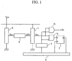
- FIG. 1 is a block diagram illustrative of a circuit configuration of a first novel voltage detecting circuit in a first embodiment in accordance with the present invention.
- the first novel voltage detecting circuit is accommodated in a single chip microcomputer.
- the first novel voltage detecting circuit comprises a low voltage detecting circuit 1, a high voltage detecting circuit 2, a latch circuit 3, a resistor 4, a logic gate 5, an AND gate 6, a flag 7, and an internal data bus 8.
- the low voltage detecting circuit 1 is connected between a high voltage line for supplying a power voltage Vdd and a ground line for supplying a ground potential.
- the high voltage detecting circuit 2 is also connected between the high voltage line for supplying the power voltage Vdd and the ground line for supplying the ground potential.
- the latch circuit 3 has an input terminal which is connected to an output terminal of the high voltage detecting circuit 2.
- the latch circuit 3 has an input terminal which is connected to an output terminal of the low voltage detecting circuit 1.
- the low voltage detecting circuit 1 is provided for detecting that the power voltage Vdd is dropped to a lower voltage level than a first reference voltage level Vref1 which has been predetermined.
- the low voltage detecting circuit 1 detects that the power voltage Vdd is dropped to a lower voltage level than the first reference voltage level Vref1, then the low voltage detecting circuit 1 is operated to output a high level output signal as a first detection signal SD1.
- the high voltage detecting circuit 2 is provided for detecting that the power voltage Vdd is dropped to a voltage level lower than a second reference voltage level Vref2 which has been predetermined but higher than the first reference voltage level Vref1. This second reference voltage level Vref2 is higher than the first reference voltage level Vref1.
- the high voltage detecting circuit 2 detects that the power voltage Vdd is dropped to a voltage level lower than the second reference voltage level Vref2 but higher than the first reference voltage level Vref1, then the high voltage detecting circuit 2 is operated to output a high level output signal as a second detection signal SD2.
- the latch circuit 3 receives the second detecting signal SD2 from the high voltage detecting circuit 2 for temporary storing or latching the same and subsequent outputting data DT2.
- the latch circuit 3 continues to latch the second detecting data SD2 once the second detecting data SD2 becomes high level.
- the low voltage detecting circuit 1 receives the data DT2 from the latch circuit 3. If the low voltage detecting circuit 1 receives the data DT2 in high level, then the low voltage detecting circuit 1 is placed into an operable state. If, however, the low voltage detecting circuit 1 receives the data DT2 in low level, then the low voltage detecting circuit 1 is placed into an inoperable state. The low voltage detecting circuit 1 is operated to output a first detecting signal SD1.
- the resister 4 has an input terminal which is connected to the internal data bus 8.
- the internal data bus 8 is provided for transmitting any interactions from the CPU core which is not illustrated.
- the resister 4 receives any instructions transmitted via the internal data bus 8 for setting its stored content to be either high level "H” or low level “L” in accordance with the received instruction.
- the logic gate 5 has first and second input terminals.
- the first input terminal of the logic gate 5 is connected to an output terminal of the low voltage detecting circuit 1 for receiving the first detecting signal SD1 from the low voltage detecting circuit 1.
- the second input terminal of the logic gate 5 is connected to an output terminal of the resistor 4 for receiving an inverted signal to the output signal of either high level "H” or low level “L” from the resister 4.
- the logic gate 5 performs AND operation of the first detecting signal SD1 and the inverted signal.
- the logic gate 5 outputs an output signal as a result of the AND operation.
- the AND gate 6 has first and second input terminals.
- the first input terminal of the AND gate 6 is also connected to an output terminal of the low voltage detecting circuit 1 for receiving the first detecting signal SD1 from the low voltage detecting circuit 1.
- the second input terminal of the AND gate 6 is also connected to the output terminal of the resistor 4 for receiving a non-inverted signal to the output signal of either high level "H” or low level “L” from the resister 4.
- the AND gate 6 performs AND operation of the first detecting signal SD1 and the non-inverted signal.
- the AND gate 6 outputs an internal reset signal SR as a result of the AND operation.
- the flag 7 comprises a flip flop circuit of set/reset type.
- the flag 7 has two input terminals "S" and “R” and a single output terminal "Q".
- the first input terminal “S” of the flag 7 is connected to the output terminal of the logic gate 5 for receiving the output signal from the logic gate 5. If the first input terminal "S” of the flag 7 receives a high level signal "H" from the logic gate 5, then the flag 7 is set to enter into a high level "H”.
- the second input terminal “R” of the flag 7 is connected to the internal data bus 8 for receiving the instruction from the CPU core so that the flag 7 is reset to enter into a low level "L”.
- the single output terminal "Q" of the flag 7 is connected to the internal data bus 8 so as to allow the content of the flag 7 to be read out in accordance with a read out instruction which has been transmitted via the internal data bus from the CPU core.
- Operational modes of the first novel voltage detecting circuit may be classified into first and second modes.
- the initial power voltage level VDDB is set to be higher than the second reference voltage level Vref2.
- the initial power voltage level VDDB is set to be lower than the second reference voltage level Vref2.
- the operation in the first mode of the first novel voltage detecting circuit placed in a first initial state will be described.
- the data DT2 from the latch circuit 3 are set to be low level "L", and thus the low voltage detecting circuit 1 is in the inoperable state.
- the flag 7 has been reset to be the low level "L” in accordance with the instruction which has been transmitted via the internal data bus 8 from the CPU core.
- the content stored in the resister 4 is set to be the low level "L".
- the initial power voltage level VDDB is set to be higher than the second reference voltage level Vref2, whereby the high voltage detecting circuit 2 detects that the power voltage level is higher than the second reference voltage level Vref2.
- the high voltage detecting circuit 2 outputs a low level output signal as the second detection signal SD2.
- the second detection signal SD2 Prior to this detection by the high voltage detecting circuit 2, however, the second detection signal SD2 was the high level, for which reason the latch circuit 3 latches the high level as the second detection signal SD2 to continue outputting the high level data as the output data DT2 even the high voltage detecting circuit 2 currently outputs a low level output signal as the second detection signal SD2.
- the low voltage detecting circuit 1 is kept to receive the high level data DT2 from the latch circuit 3 even after the high voltage detecting circuit 2 has detected that the power voltage level has become higher than the second reference voltage level Vref2.
- the low voltage detecting circuit 1 detects that the power voltage level VDD is lower than the first reference voltage level Vref1.
- the low voltage detecting circuit 1 outputs the first detection signal SD1 of the high level "H”.
- the first detection signal SD1 of the high level "H” is then transmitted through the logic gate 5 to the flag 7 so that the flag 7 is set to be the high level "H”.
- the CPU core sends a read out instruction through the internal data bus 8 to the flag 7, whereby the high level "H” of the flag 7 is red out. Accordingly, the drop of the power voltage VDD down to the first reference voltage level Vref1 can be recognized by the CPU core.
- the CPU core therefore perform the necessary processing such as reset operations for preventing malfunction of the microcomputer.
- the content stored in the resister 4 has been set to be the low level "L” in the initial state, for which reason the first detection signal SD1 of he high level “H” does not pass through the AND gate 6, whereby the internal reset signal SR remains low level "L".
- the operation in the first mode of the first novel voltage detecting circuit placed in a second initial state will be described.
- the data DT2 from the latch circuit 3 are set to be low level "L", and thus the low voltage detecting circuit 1 is in the inoperable state.
- the flag 7 has been reset to be the low level "L” in accordance with the instruction which has been transmitted via the internal data bus 8 from the CPU core.
- the content stored in the resister 4 is set to be the high level "H".
- the initial power voltage level VDDB is set to be higher than the second reference voltage level Vref2, whereby the high voltage detecting circuit 2 detects that the power voltage level is higher than the second reference voltage level Vref2.
- the high voltage detecting circuit 2 outputs a low level output signal as the second detection signal SD2.
- the second detection signal SD2 Prior to this detection by the high voltage detecting circuit 2, however, the second detection signal SD2 was the high level, for which reason the latch circuit 3 latches the high level as the second detection signal SD2 to continue outputting the high level data as the output data DT2 even the high voltage detecting circuit 2 currently outputs a low level output signal as the second detection signal SD2.
- the low voltage detecting circuit 1 is kept to receive the high level data DT2 from the latch circuit 3 even after the high voltage detecting circuit 2 has detected that the power voltage level has become higher than the second reference voltage level Vref2.
- the low voltage detecting circuit 1 detects that the power voltage level VDD is lower than the first reference voltage level Vref1.
- the low voltage detecting circuit 1 outputs the first detection signal SD1 of the high level "H”.
- the first detection signal SD1 of the high level "H” is then transmitted through the AND gate 6 whereby the internal reset signal SR of the high level "H” is outputted from the AND gate 6.
- the CPU core and other internal circuits in the microcomputer can recognize that the power voltage level VDD is lower than the first reference voltage level Vref1 in accordance with the internal reset signal SR of the high level "H".
- the CPU core therefore perform the necessary processing such as reset operations for preventing malfunction of the microcomputer.
- the content stored in the resister 4 has been set to be the high level "H” in the initial state, for which reason the first detection signal SD1 of he high level "H” does not pass through the logic gate 5, whereby the flag 7 remains low level "L".
- the operation in the second mode of the first novel voltage detecting circuit will be described.
- the data DT2 from the latch circuit 3 are set to be low level "L", and thus the low voltage detecting circuit 1 is in the inoperable state.
- the flag 7 has been reset to be the low level "L” in accordance with the instruction which has been transmitted via the internal data bus 8 from the CPU core.
- the initial power voltage level VDDB is set to be lower than the second reference voltage level Vref2, whereby the high voltage detecting circuit 2 detects that the power voltage level is lower than the second reference voltage level Vref2.
- the high voltage detecting circuit 2 continues to output a low level output signal as the second detection signal SD2.
- the latch circuit 3 keeps the initial state to continue to output low level data DT2.
- the low voltage detecting circuit 1 continues to receive the low level data DT2 from the latch circuit 3, whereby the low voltage detecting circuit 1 is kept in the inoperable state.
- the low voltage detecting circuit 1 is kept in the inoperable state, for which reason the low voltage detecting circuit 1 does not detect that the power voltage level VDD is lower than the first reference voltage level Vref1.
- the flag 7 is kept reset in the low level "L” whilst the internal reset signal SR is also kept to be low level "L".
- the CPU core and the other internal circuits in the microcomputer does not recognizes the drop of the power voltage, whereby no reset operation is executed to allow the other circuits in the microcomputer to continue the normal operations.
- the low voltage detecting circuit is operable. If, however, the initial power voltage level is set to be lower than the second reference voltage level, then the low voltage detecting circuit is inoperable. Namely, setting the initial power voltage level with reference to the second reference voltage level can control the low voltage detecting circuit to be operable or inoperable state even after the microcomputer has been manufactured.
- the above first novel voltage detecting circuit is applicable to not only the microcomputer such as the mask programmable ROM type microcomputer capable of designating the mask option but also other microcomputer such as the EPROM type microcomputer incapable of designating the mask option.
- the above first novel voltage detecting circuit makes it possible to set the low voltage detecting circuit to be operable or inoperable state without using any program, whereby programs may be made common even in the microcomputer using different power voltages.
- FIG. 2 is a block diagram illustrative of a circuit configuration of a second novel voltage detecting circuit in a second embodiment in accordance with the present invention.
- the second novel voltage detecting circuit is accommodated in a single chip microcomputer.
- the second novel voltage detecting circuit comprises a first low voltage detecting circuit 11, a second low voltage detecting circuit 12, a high voltage detecting circuit 13, a latch circuit 14, a selector 15, a resistor 16, a logic gate 17, an AND gate 18, a flag 19, and an internal data bus 20.
- the first low voltage detecting circuit 11 is connected between a high voltage line for supplying a power voltage Vdd and a ground line for supplying a ground potential.
- the second low voltage detecting circuit 11 is also connected between a high voltage line for supplying a power voltage Vdd and a ground line for supplying a ground potential.
- the high voltage detecting circuit 13 is also connected between the high voltage line for supplying the power voltage Vdd and the ground line for supplying the ground potential.
- the latch circuit 14 has an input terminal which is connected to an output terminal of the high voltage detecting circuit 13.
- the latch circuit 14 has an output terminal which is connected to an input terminal of the first low voltage detecting circuit 11 and also connected to an input terminal of the second low voltage detecting circuit 12.
- the first low voltage detecting circuit 11 is provided for detecting that the power voltage Vdd is dropped to a lower voltage level than a first reference voltage level Vref1 which has been predetermined. If the first low voltage detecting circuit 11 detects that the power voltage Vdd is dropped to a lower voltage level than the first reference voltage level Vref1, then the first low voltage detecting circuit 11 is operated to output a high level output signal as a first detection signal SD1.
- the second low voltage detecting circuit 12 is provided for detecting that the power voltage Vdd is dropped to a lower voltage level than a second reference voltage level Vref2 which has been predetermined, wherein the second reference voltage level Vref2 is lower than the first reference voltage level Vref1. If the second low voltage detecting circuit 12 detects that the power voltage Vdd is dropped to a lower voltage level than the second reference voltage level Vref2, then the second low voltage detecting circuit 12 is operated to output a high level output signal as a second detection signal SD2.
- the high voltage detecting circuit 13 is provided for detecting that the power voltage Vdd is higher than a third reference voltage level Vref3 which has been predetermined but higher than the first reference voltage level Vref1.
- This third reference voltage level Vref3 is higher than the first reference voltage level Vref1. If the high voltage detecting circuit 13 detects that the power voltage Vdd is higher than the third reference voltage level Vref3, then the high voltage detecting circuit 13 is operated to output a high level output signal as a third detection signal SD3.
- the latch circuit 14 receives the third detecting signal SD3 from the high voltage detecting circuit 13 for temporary storing or latching the same and subsequent outputting data DT3.
- the latch circuit 14 continues to latch the third detecting data SD3 once the third detecting data SD3 become high level.
- the first low voltage detecting circuit 11 receives the data DT3 from the latch circuit 14. If the first low voltage detecting circuit 11 receives the data DT3 in high level, then the first low voltage detecting circuit 11 is placed into an operable state. If, however, the first low voltage detecting circuit 11 receives the data DT3 in low level, then the first low voltage detecting circuit 11 is placed into an inoperable state. The first low voltage detecting circuit 11 is operated to output a first detecting signal SD1.
- the second low voltage detecting circuit 12 receives an inverted signal to the data DT3 from the latch circuit 14. If the second low voltage detecting circuit 12 receives the data DT3 in high level, then the second low voltage detecting circuit 12 is placed into an inoperable state. If, however, the second low voltage detecting circuit 12 receives the data DT3 in low level, then the second low voltage detecting circuit 12 is placed into an operable state. The second low voltage detecting circuit 12 is operated to output a second detecting signal SD2.
- the selector 15 has first and second input terminals, a control terminal and an output terminal.
- the first terminal of the selector 15 is connected to the output terminal of the first low voltage detecting circuit 11 for receiving the first detecting signal SD1 from the first low voltage detecting circuit 11.
- the second terminal of the selector 15 is connected to the output terminal of the second low voltage detecting circuit 12 for receiving the second detecting signal SD2 from the second low voltage detecting circuit 12.
- the control terminal of the selector 15 is connected to the output terminal of the latch circuit 14 for receiving the data DT3 from the latch circuit 14.
- the selector 15 selects the first detecting signal SD1 to output the same from the output terminal thereof.
- the selector 15 selects the second detecting signal SD2 to output the same from the output terminal thereof.
- the resister 16 has an input terminal which is connected to the internal data bus 20.
- the internal data bus 20 is provided for transmitting any interactions from the CPU core which is not illustrated.
- the resister 16 receives any instructions transmitted via the internal data bus 20 for setting its stored content to be either high level "H” or low level “L” in accordance with the received instruction.
- the logic gate 17 has first and second input terminals.
- the first input terminal of the logic gate 17 is connected to an output terminal of the selector 15 for receiving selected one of the first and second detecting signals SD1 and SD2 from the selector 15.
- the second input terminal of the logic gate 17 is connected to an output terminal of the resistor 16 for receiving an inverted signal to the output signal of either high level "H” or low level “L” from the resister 16.
- the logic gate 17 performs AND operation of the selected one of the first and second detecting signals SD1 and SD2 and the inverted signal.
- the logic gate 17 outputs an output signal as a result of the AND operation.
- the AND gate 18 has first and second input terminals.
- the first input terminal of the AND gate 18 is also connected to an output terminal of the selector 15 for receiving selected one of the first and second detecting signals SD1 and SD2 from the selector 15.
- the second input terminal of the AND gate 18 is also connected to the output terminal of the resistor 16 for receiving a non-inverted signal to the output signal of either high level "H” or low level “L” from the resister 16.
- the AND gate 18 performs AND operation of the selected one of the first and second detecting signals SD1 and SD2 and the non-inverted signal.
- the AND gate 18 outputs an internal reset signal SR as a result of the above AND operation.
- the flag 19 comprises a flip flop circuit of set/reset type.
- the flag 19 has two input terminals "S" and “R” and a single output terminal "Q".
- the first input terminal “S” of the flag 19 is connected to the output terminal of the logic gate 17 for receiving the output signal from the logic gate 17. If the first input terminal "S” of the flag 19 receives a high level signal "H" from the logic gate 17, then the flag 19 is set to enter into a high level "H”.
- the second input terminal “R” of the flag 19 is connected to the internal data bus 20 for receiving the instruction from the CPU core so that the flag 19 is reset to enter into a low level "L”.
- the single output terminal "Q" of the flag 19 is connected to the internal data bus 20 so as to allow the content of the flag 19 to be read out in accordance with a read out instruction which has been transmitted via the internal data bus from the CPU core.
- Operational modes of the second novel voltage detecting circuit may be classified into first and second modes.
- the initial power voltage level VDDB is set to be higher than the third reference voltage level Vref3.
- the initial power voltage level VDDB is set to be lower than the third reference voltage level Vref3.
- the operation in the first mode of the second novel voltage detecting circuit placed in a first initial state will be described.
- the data DT3 from the latch circuit 14 are set to be low level "L”, and thus the first low voltage detecting circuit 11 is in the inoperable state, whilst the second low voltage detecting circuit 12 is in the operable state.
- the flag 19 has been reset to be the low level “L” in accordance with the instruction which has been transmitted via the internal data bus 20 from the CPU core.
- the content stored in the resister 16 is set to be the low level "L".
- the initial power voltage level VDDB is set to be higher than the third reference voltage level Vref3, whereby the high voltage detecting circuit 13 detects that the power voltage level is higher than the third reference voltage level Vref3.
- the high voltage detecting circuit 13 outputs a high level output signal as the third detection signal SD3.
- the third detection signal SD3 Prior to this detection by the high voltage detecting circuit 13, however, the third detection signal SD3 was the high level, for which reason the latch circuit 14 latches the high level as the third detection signal SD3 to continue outputting the high level data as the output data DT3 even the high voltage detecting circuit 13 currently outputs a low level output signal as the third detection signal SD3.
- the high level data as the output data DT3 is transmitted to the first and second low voltage detecting circuits 11 and 12 and the selector 15.
- the first low voltage detecting circuit 11 is placed into the operable state, whilst the second low voltage detecting circuit 12 is placed into the operable state.
- the selector 15 receives the high level data DT3 and thus the selector 15 is placed into such a state as to select the first detecting signal SD1 which has been received from the low voltage detecting circuit 11.
- the high voltage detecting circuit 13 detects that the power voltage level VDD is lower than the third reference voltage level Vref3.
- the high voltage detecting circuit 13 outputs the third detection signal SD3 of the low level "L".
- the latch circuit 14 Prior to the detection by the high voltage detecting circuit 13, once the data DT3 has been the high level, for which reason the latch circuit 14 continues to latch the high level data DT3 and to send the high level data DT3 to the first and second low voltage detecting circuits 11 and 12 and the selector 15.
- the first low voltage detecting circuit 11 detects that the power voltage level VDD is lower than the first reference voltage level Vref1.
- the first low voltage detecting circuit 11 outputs the first detection signal SD1 of the high level "H”.
- the first detection signal SD1 of the high level "H” is then transmitted through the selector 15 and the logic gate 17 to the flag 19 so that the flag 19 is set to be the high level "H”.
- the CPU core sends a read out instruction through the internal data bus 20 to the flag 19, whereby the high level "H” of the flag 19 is red out. Accordingly, the drop of the power voltage VDD down to the first reference voltage level Vref1 can be recognized by the CPU core.
- the CPU core therefore perform the necessary processing such as reset operations for preventing malfunction of the microcomputer.
- the content stored in the resister 16 has been set to be the low level "L” in the initial state, for which reason the first detection signal SD1 of he high level “H” does not pass through the AND gate 18, whereby the internal reset signal SR remains low level "L".
- the operation in the first mode of the second novel voltage detecting circuit placed in a second initial state will be described.
- the data DT3 from the latch circuit 14 are set to be low level "L", and thus the first low voltage detecting circuit 11 is in the inoperable state, whilst the second low voltage detecting circuit 12 is in the operable state.
- the flag 19 has been reset to be the low level "L” in accordance with the instruction which has been transmitted via the internal data bus 20 from the CPU core.
- the content stored in the resister 16 is set to be the high level "H".
- the initial power voltage level VDDB is set to be higher than the third reference voltage level Vref3, whereby the high voltage detecting circuit 13 detects that the power voltage level is higher than the third reference voltage level Vref3.
- the high voltage detecting circuit 13 outputs a high level output signal as the third detection signal SD3.
- the third detection signal SD3 Prior to this detection by the high voltage detecting circuit 13, however, the third detection signal SD3 was the high level, for which reason the latch circuit 14 latches the high level as the third detection signal SD3 to continue outputting the high level data as the output data DT3 even the high voltage detecting circuit 13 currently outputs a low level output signal as the third detection signal SD3.
- the high level data as the output data DT3 is transmitted to the first and second low voltage detecting circuits 11 and 12 and the selector 15.
- the first low voltage detecting circuit 11 is placed into the operable state, whilst the second low voltage detecting circuit 12 is placed into the operable state.
- the selector 15 receives the high level data DT3 and thus the selector 15 is placed into such a state as to select the first detecting signal SD1 which has been received from the low voltage detecting circuit 11.
- the first low voltage detecting circuit 11 detects that the power voltage level VDD is lower than the first reference voltage level Vref1.
- the first low voltage detecting circuit 11 outputs the first detection signal SD1 of the high level "H”.
- the first detection signal SD1 of the high level "H” is then transmitted through the AND gate 18 whereby the internal reset signal SR of the high level "H” is outputted from the AND gate 18.
- the CPU core and other internal circuits in the microcomputer can recognize that the power voltage level VDD is lower than the first reference voltage level Vref1 in accordance with the internal reset signal SR of the high level "H".
- the CPU core therefore perform the necessary processing such as reset operations for preventing malfunction of the microcomputer.
- the content stored in the resister 16 has been set to be the high level "H” in the initial state, for which reason the first detection signal SD1 of he high level "H” does not pass through the logic gate 17, whereby the flag 19 remains low level "L".
- the operation in the first mode of the second novel voltage detecting circuit placed in a first initial state will be described.
- the data DT3 from the latch circuit 14 are set to be low level "L”, and thus the first low voltage detecting circuit 11 is in the operable state, whilst the second low voltage detecting circuit 12 is in the inoperable state.
- the flag 19 has been reset to be the low level “L” in accordance with the instruction which has been transmitted via the internal data bus 20 from the CPU core.
- the content stored in the resister 16 is set to be the low level "L".
- the initial power voltage level VDDB is set to be lower than the third reference voltage level Vref3, whereby the high voltage detecting circuit 13 detects that the power voltage level is higher than the third reference voltage level Vref3.
- the high voltage detecting circuit 13 outputs a low level output signal as the third detection signal SD3, for which reason the latch circuit 14 latches the low level as the third detection signal SD3 to continue outputting the low level data as the output data DT3.
- the low level data as the output data DT3 are transmitted to the first and second low voltage detecting circuits 11 and 12 and the selector 15.
- the first low voltage detecting circuit 11 remains in the inoperable state, whilst the second low voltage detecting circuit 12 remains in the operable state.
- the selector 15 receives the low level data DT3 and thus the selector 15 is placed into such a state as to select the second detecting signal SD2 which has been received from the second low voltage detecting circuit 12.
- the first low voltage detecting circuit 11 remains inoperable state so that the first low voltage detecting circuit 11 does not detect that the power voltage level VDD is lower than the first reference voltage level Vref1.
- the second low voltage detecting circuit 12 is in operable state, but the second low voltage detecting circuit 12 outputs the low level detecting signal SD2 because the power voltage VDD is higher than the second reference voltage level Vref2.
- the second low voltage detecting circuit 12 detects that the power voltage level VDD is lower than the second reference voltage level Vref2.
- the second low voltage detecting circuit 12 outputs the second detection signal SD2 of the high level "H".
- the second detection signal SD2 of the high level "H” is then transmitted through the selector 15 and the logic gate 17 to the flag 19 so that the flag 19 is set to be the high level "H”.
- the CPU core sends a read out instruction through the internal data bus 20 to the flag 19, whereby the high level "H” of the flag 19 is red out. Accordingly, the drop of the power voltage VDD down to the second reference voltage level Vref2 can be recognized by the CPU core.
- the CPU core therefore perform the necessary processing such as reset operations for preventing malfunction of the microcomputer.
- the content stored in the resister 16 has been set to be the low level "L” in the initial state, for which reason the second detection signal SD2 of he high level “H” does not pass through the AND gate 18, whereby the internal reset signal SR remains low level "L".
- the operation in the first mode of the second novel voltage detecting circuit placed in a second initial state will be described.
- the data DT3 from the latch circuit 14 are set to be low level "L", and thus the first low voltage detecting circuit 11 is in the inoperable state, whilst the second low voltage detecting circuit 12 is in the operable state.
- the flag 19 has been reset to be the low level "L” in accordance with the instruction which has been transmitted via the internal data bus 20 from the CPU core.
- the content stored in the resister 16 is set to be the high level "H".
- the initial power voltage level VDDB is set to be lower than the third reference voltage level Vref3, whereby the high voltage detecting circuit 13 detects that the power voltage level is higher than the third reference voltage level Vref3.
- the high voltage detecting circuit 13 outputs a low level output signal as the third detection signal SD3, for which reason the latch circuit 14 latches the low level as the third detection signal SD3 to continue outputting the low level data as the output data DT3.
- the low level data as the output data DT3 are transmitted to the first and second low voltage detecting circuits 11 and 12 and the selector 15.
- the first low voltage detecting circuit 11 remains in the inoperable state, whilst the second low voltage detecting circuit 12 remains in the operable state.
- the selector 15 receives the low level data DT3 and thus the selector 15 is placed into such a state as to select the second detecting signal SD2 which has been received from the second low voltage detecting circuit 12.
- the second low voltage detecting circuit 12 detects that the power voltage level VDD is lower than the second reference voltage level Vref2.
- the second low voltage detecting circuit 12 outputs the second detection signal SD2 of the high level "H”.
- the second detection signal SD2 of the high level "H” is then transmitted through the AND gate 18 whereby the internal reset signal SR of the high level "H” is outputted from the AND gate 18.
- the CPU core and other internal circuits in the microcomputer can recognize that the power voltage level VDD is lower than the second reference voltage level Vref2 in accordance with the internal reset signal SR of the high level "H".
- the CPU core therefore performs the necessary processing such as reset operations for preventing malfunction of the microcomputer.
- the content stored in the resister 16 has been set to be the high level "H” in the initial state, for which reason the first detection signal SD1 of the high level "H” does not pass through the logic gate 17, whereby the flag 19 remains low level "L".
- the initial power voltage level VDDB is set higher or lower than the third reference voltage level Vref3, so that the first and second low voltage detecting circuits 11 and 12 are set to be operable/inoperable states or inoperable/operable states.
- the initial power voltage VDDB is set lower than the third reference voltage Vref3, then it is possible to detect that the power voltage VDD is dropped into a lower voltage level than the second refence voltage Vref2.
- the CPU core and the other circuits of the microcomputer can recognize the drop of the power voltage level. Independently from the contents stored in the resister 16, the flag 19 is kept reset in the low level "L" whilst the internal reset signal SR is also kept to be low level "L".
- the CPU core and the other internal circuits in the microcomputer does not recognizes the drop of the power voltage, whereby no reset operation is executed to allow the other circuits in the microcomputer to continue the normal operations.
- the high voltage detecting circuit detects that an excess high voltage is applied to the high voltage detecting circuit for preventing the break down of the circuit to improve the safety.
- the output signal from the logic gate is used as the internal reset signal. It is, however, possible to use the output signal as an interrupt request signal for interrupting operations by the CPU core.
- the above first and second novel voltage detecting circuit may be applicable to not only the single chip microcomputer but also other electronic devices such as semiconductor memories, for example, RAM and ROM as other electronic circuits such as digital signal processors so that the circuit configuration other than the power circuit and the program are made common.
Landscapes
- Physics & Mathematics (AREA)
- General Physics & Mathematics (AREA)
- Engineering & Computer Science (AREA)
- Theoretical Computer Science (AREA)
- General Engineering & Computer Science (AREA)
- Power Sources (AREA)
- Microcomputers (AREA)
- Electronic Switches (AREA)
- Measurement Of Current Or Voltage (AREA)
- Semiconductor Integrated Circuits (AREA)
Applications Claiming Priority (2)
| Application Number | Priority Date | Filing Date | Title |
|---|---|---|---|
| JP33179298 | 1998-11-20 | ||
| JP33179298A JP3230502B2 (ja) | 1998-11-20 | 1998-11-20 | 電圧検出回路 |
Publications (1)
| Publication Number | Publication Date |
|---|---|
| EP1003046A1 true EP1003046A1 (de) | 2000-05-24 |
Family
ID=18247701
Family Applications (1)
| Application Number | Title | Priority Date | Filing Date |
|---|---|---|---|
| EP99123157A Withdrawn EP1003046A1 (de) | 1998-11-20 | 1999-11-22 | Spannungsdetektorschaltung |
Country Status (5)
| Country | Link |
|---|---|
| US (1) | US6222398B1 (de) |
| EP (1) | EP1003046A1 (de) |
| JP (1) | JP3230502B2 (de) |
| KR (1) | KR100339257B1 (de) |
| CN (1) | CN1118006C (de) |
Families Citing this family (8)
| Publication number | Priority date | Publication date | Assignee | Title |
|---|---|---|---|---|
| KR100293523B1 (ko) * | 1998-02-25 | 2001-09-17 | 구본준, 론 위라하디락사 | 액정표시장치 |
| KR100351990B1 (ko) * | 2000-09-29 | 2002-09-12 | 주식회사 하이닉스반도체 | 저전압 검출회로 |
| KR100416374B1 (ko) * | 2001-04-26 | 2004-01-31 | 삼성전자주식회사 | 마이크로 컨트롤러용 저전압 리셋 회로 |
| JP3933467B2 (ja) | 2001-12-27 | 2007-06-20 | 株式会社東芝 | 電圧検出回路制御装置、同装置を有するメモリー制御装置及び同装置を有するメモリーカード |
| KR100463201B1 (ko) | 2002-05-28 | 2004-12-23 | 삼성전자주식회사 | 파워 검출 회로, 이를 이용한 플래시 메모리 장치, 그 플래시 메모리 장치의 파워-온 독출 신호 발생 방법 및 플래시 메모리 장치의 안정적인 파워-온 독출 방법 |
| KR100882426B1 (ko) * | 2002-06-24 | 2009-02-05 | 매그나칩 반도체 유한회사 | 전원전압 검출회로 |
| CN101871963A (zh) * | 2010-05-28 | 2010-10-27 | 上海宏力半导体制造有限公司 | 电源电压检测电路 |
| CN109313225B (zh) * | 2018-09-21 | 2019-10-01 | 长江存储科技有限责任公司 | 电压检测系统 |
Citations (4)
| Publication number | Priority date | Publication date | Assignee | Title |
|---|---|---|---|---|
| JPS60211370A (ja) * | 1984-04-05 | 1985-10-23 | Toshiba Corp | 電圧検出回路 |
| JPH0197133A (ja) * | 1987-10-05 | 1989-04-14 | Mitsubishi Electric Corp | 電源保護装置 |
| JPH07322682A (ja) * | 1994-03-31 | 1995-12-08 | Mitsubishi Electric Corp | モータの駆動制御装置 |
| US5541551A (en) * | 1994-12-23 | 1996-07-30 | Advinced Micro Devices, Inc. | Analog voltage reference generator system |
Family Cites Families (7)
| Publication number | Priority date | Publication date | Assignee | Title |
|---|---|---|---|---|
| US3950175A (en) | 1973-11-05 | 1976-04-13 | Corning Glass Works | Pore size control in cordierite ceramic |
| US4031463A (en) * | 1976-03-01 | 1977-06-21 | Control Data Corporation | Power brown-out detector |
| JP2735838B2 (ja) | 1988-08-10 | 1998-04-02 | 三洋電機株式会社 | ワンチップマイクロコンピュータ |
| JP3082782B2 (ja) | 1991-03-25 | 2000-08-28 | 新日本無線株式会社 | 電圧検知回路 |
| FI97262C (fi) * | 1994-10-03 | 1996-11-11 | Nokia Mobile Phones Ltd | Tulosignaalin kynnysarvon ylityksen virtaa säästävä ilmaisu |
| US5786717A (en) * | 1995-12-22 | 1998-07-28 | Holtek Microelectronics Inc. | System reset device having level controller for opportunely setting system reset status |
| JPH10198466A (ja) | 1997-01-10 | 1998-07-31 | Nec Home Electron Ltd | 電源電圧監視用ic |
-
1998
- 1998-11-20 JP JP33179298A patent/JP3230502B2/ja not_active Expired - Fee Related
-
1999
- 1999-11-19 KR KR1019990051514A patent/KR100339257B1/ko not_active Expired - Fee Related
- 1999-11-22 US US09/444,906 patent/US6222398B1/en not_active Expired - Lifetime
- 1999-11-22 EP EP99123157A patent/EP1003046A1/de not_active Withdrawn
- 1999-11-22 CN CN99123974A patent/CN1118006C/zh not_active Expired - Fee Related
Patent Citations (4)
| Publication number | Priority date | Publication date | Assignee | Title |
|---|---|---|---|---|
| JPS60211370A (ja) * | 1984-04-05 | 1985-10-23 | Toshiba Corp | 電圧検出回路 |
| JPH0197133A (ja) * | 1987-10-05 | 1989-04-14 | Mitsubishi Electric Corp | 電源保護装置 |
| JPH07322682A (ja) * | 1994-03-31 | 1995-12-08 | Mitsubishi Electric Corp | モータの駆動制御装置 |
| US5541551A (en) * | 1994-12-23 | 1996-07-30 | Advinced Micro Devices, Inc. | Analog voltage reference generator system |
Non-Patent Citations (3)
| Title |
|---|
| PATENT ABSTRACTS OF JAPAN vol. 010, no. 072 (P - 438) 22 March 1986 (1986-03-22) * |
| PATENT ABSTRACTS OF JAPAN vol. 013, no. 333 (E - 794) 26 July 1989 (1989-07-26) * |
| PATENT ABSTRACTS OF JAPAN vol. 1996, no. 04 30 April 1996 (1996-04-30) * |
Also Published As
| Publication number | Publication date |
|---|---|
| US6222398B1 (en) | 2001-04-24 |
| KR100339257B1 (ko) | 2002-05-31 |
| KR20000035580A (ko) | 2000-06-26 |
| CN1254873A (zh) | 2000-05-31 |
| JP2000155140A (ja) | 2000-06-06 |
| CN1118006C (zh) | 2003-08-13 |
| JP3230502B2 (ja) | 2001-11-19 |
Similar Documents
| Publication | Publication Date | Title |
|---|---|---|
| US4010449A (en) | Mos computer employing a plurality of separate chips | |
| US6094367A (en) | Voltage regulating device for dynamically regulating voltage in a computer system | |
| US5969529A (en) | Electronic apparatus having battery power source | |
| US4384326A (en) | Memory security circuit using the simultaneous occurance of two signals to enable the memory | |
| US5336947A (en) | Discriminator device | |
| US10817452B2 (en) | Bus system and detection method thereof | |
| JPH10206472A (ja) | 自動範囲決定低電圧検出回路 | |
| US6222398B1 (en) | Voltage detecting circuit | |
| US8395424B2 (en) | Semiconductor device and operation mode switch method | |
| KR880014482A (ko) | 반도체 집적회로 장치 | |
| JPH04178114A (ja) | 電子機器 | |
| EP0377455B1 (de) | Prüfmodusumschaltsystem für LSI | |
| KR100314413B1 (ko) | 내부상태확정장치및집적회로카드 | |
| US20060112290A1 (en) | Vehicle-installed microcomputer system | |
| US6796501B2 (en) | Smart card reader circuit and method of monitoring | |
| EP3637571B1 (de) | Schaltung mit warnung vor kritischen betriebszuständen, entsprechende vorrichtung und verfahren | |
| US4769781A (en) | IC device compatible with input signals in the formats for two-line and four-line type bus lines | |
| US6650579B1 (en) | Semiconductor device having test and read modes and protection such that ROM data reading is prevented in the test mode | |
| KR19980083379A (ko) | 자동 리셋 기능을 갖는 스마트 카드 | |
| US9218298B2 (en) | Electronic device system and storage device | |
| US6378034B1 (en) | Microcomputer with flash EEPROM having automatic communication mode determining function | |
| US6430630B1 (en) | Direct data access between input and output ports | |
| JP2003016400A (ja) | 停電検知装置、及びその停電検知装置を備えたカードリーダ | |
| JP2008118226A (ja) | 検出センサ、コントローラ、及びセンサシステム | |
| JPH03182950A (ja) | 電子機器の停電処理装置 |
Legal Events
| Date | Code | Title | Description |
|---|---|---|---|
| PUAI | Public reference made under article 153(3) epc to a published international application that has entered the european phase |
Free format text: ORIGINAL CODE: 0009012 |
|
| 17P | Request for examination filed |
Effective date: 20000228 |
|
| AK | Designated contracting states |
Kind code of ref document: A1 Designated state(s): DE GB |
|
| AX | Request for extension of the european patent |
Free format text: AL;LT;LV;MK;RO;SI |
|
| AKX | Designation fees paid |
Free format text: DE GB |
|
| RAP1 | Party data changed (applicant data changed or rights of an application transferred) |
Owner name: NEC ELECTRONICS CORPORATION |
|
| 17Q | First examination report despatched |
Effective date: 20040419 |
|
| GRAP | Despatch of communication of intention to grant a patent |
Free format text: ORIGINAL CODE: EPIDOSNIGR1 |
|
| STAA | Information on the status of an ep patent application or granted ep patent |
Free format text: STATUS: THE APPLICATION IS DEEMED TO BE WITHDRAWN |
|
| 18D | Application deemed to be withdrawn |
Effective date: 20050530 |