EP1003217A2 - Réseau de résistances régulé, dispositif semi-conducteur comprenant ce réseau de résistance, et méthode de fabrication - Google Patents
Réseau de résistances régulé, dispositif semi-conducteur comprenant ce réseau de résistance, et méthode de fabrication Download PDFInfo
- Publication number
- EP1003217A2 EP1003217A2 EP99122167A EP99122167A EP1003217A2 EP 1003217 A2 EP1003217 A2 EP 1003217A2 EP 99122167 A EP99122167 A EP 99122167A EP 99122167 A EP99122167 A EP 99122167A EP 1003217 A2 EP1003217 A2 EP 1003217A2
- Authority
- EP
- European Patent Office
- Prior art keywords
- resistors
- resistor network
- regulating
- resistor
- thin
- Prior art date
- Legal status (The legal status is an assumption and is not a legal conclusion. Google has not performed a legal analysis and makes no representation as to the accuracy of the status listed.)
- Granted
Links
Images





Classifications
-
- H—ELECTRICITY
- H01—ELECTRIC ELEMENTS
- H01C—RESISTORS
- H01C17/00—Apparatus or processes specially adapted for manufacturing resistors
- H01C17/22—Apparatus or processes specially adapted for manufacturing resistors adapted for trimming
- H01C17/24—Apparatus or processes specially adapted for manufacturing resistors adapted for trimming by removing or adding resistive material
- H01C17/242—Apparatus or processes specially adapted for manufacturing resistors adapted for trimming by removing or adding resistive material by laser
-
- H—ELECTRICITY
- H01—ELECTRIC ELEMENTS
- H01C—RESISTORS
- H01C17/00—Apparatus or processes specially adapted for manufacturing resistors
- H01C17/22—Apparatus or processes specially adapted for manufacturing resistors adapted for trimming
- H01C17/23—Apparatus or processes specially adapted for manufacturing resistors adapted for trimming by opening or closing resistor geometric tracks of predetermined resistive values, e.g. snapistors
-
- H—ELECTRICITY
- H10—SEMICONDUCTOR DEVICES; ELECTRIC SOLID-STATE DEVICES NOT OTHERWISE PROVIDED FOR
- H10D—INORGANIC ELECTRIC SEMICONDUCTOR DEVICES
- H10D84/00—Integrated devices formed in or on semiconductor substrates that comprise only semiconducting layers, e.g. on Si wafers or on GaAs-on-Si wafers
- H10D84/201—Integrated devices formed in or on semiconductor substrates that comprise only semiconducting layers, e.g. on Si wafers or on GaAs-on-Si wafers characterised by the integration of only components covered by H10D1/00 or H10D8/00, e.g. RLC circuits
- H10D84/204—Integrated devices formed in or on semiconductor substrates that comprise only semiconducting layers, e.g. on Si wafers or on GaAs-on-Si wafers characterised by the integration of only components covered by H10D1/00 or H10D8/00, e.g. RLC circuits of combinations of diodes or capacitors or resistors
- H10D84/209—Integrated devices formed in or on semiconductor substrates that comprise only semiconducting layers, e.g. on Si wafers or on GaAs-on-Si wafers characterised by the integration of only components covered by H10D1/00 or H10D8/00, e.g. RLC circuits of combinations of diodes or capacitors or resistors of only resistors
Definitions
- the present invention relates to a regulating resistor network for regulating voltage or current supplied to a semiconductor circuit within certain limits, a semiconductor device including such a resistor network and a method for fabricating the device.
- first and second chips B and C are mounted on a printed wiring board A .
- a field effect transistor (FET) 1 is formed as an amplifier on the first chip B .
- the drain terminal of the FET 1 is connected to a drain voltage supply terminal 2 , while the source terminal thereof is grounded.
- a resistance adjustment circuit 4 for regulating a bias voltage applied to the gate terminal 3 of the FET 1 is formed on the second chip C .
- the resistance adjustment circuit 4 includes a voltage supply terminal V GG , first and second voltage dividers 5 and 6 and a trimming resistor 7 , which are connected in series to each other.
- a signal input terminal V s for applying an input voltage to the gate terminal 3 of the FET 1 is provided on the printed wiring board A .
- the trimming resistor 7 is implemented as a thin-film resistor including a plurality of notches 7a , which have been formed by laser-trimming the thin-film resistor.
- the current path has an increased length.
- the resistance value of the thin-film resistor goes on increasing gradually as the current flows over a longer distance, and the resistance value of the trimming resistor 7 is adjustable.
- the amount of a current flowing through the resistance adjustment circuit 4 also changes.
- the bias voltage applied to the gate terminal 3 of the FET 1 changes, too.
- the operating current can be regulated at the desired value by adjusting the resistance value of the trimming resistor 7 and thereby changing the bias voltage applied to the gate terminal 3 .
- a predetermined voltage is applied to the voltage supply terminal V GG of the resistance adjustment circuit 4 and a bias voltage is applied to the gate terminal 3 of the FET 1 .
- the thin-film trimming resistor 7 is laser-trimmed, thereby gradually increasing the resistance value of the trimming resistor 7 .
- the thin-film trimming resistor 7 should be laser-trimmed, while the operating current of the FET 1 is being monitored. Thus, it usually takes as long a time as 5 to 7 seconds to complete such fine adjustment.
- the trimming resistor 7 and the resistance adjustment circuit 4 both receive a large quantity of heat. Accordingly, if the resistance adjustment circuit 4 and the FET 1 are formed on the same chip, then the laser irradiation on the trimming resistor 7 causes considerable damage to the FET 1 .
- a semiconductor circuit such as the FET 1 and the resistance adjustment circuit 4 should be separately formed on the first and second chips B and C . And then these chips B and C should be mounted on the printed wiring board A . That is to say, the semiconductor circuit and resistance adjustment circuit cannot be integrated on the same chip.
- An object of the present invention is getting resistance adjustment circuit and semiconductor circuit integrated on the same chip by shortening the time taken to adjust the resistance value of the resistance adjustment circuit and by reducing the quantity of heat received by the resistance adjustment circuit during the adjustment.
- a regulating resistor network includes a plurality of resistors connected in parallel to each other. Each said resistor is cuttable by being irradiated with light, and a resistance value of the regulating resistor network is adjustable by cutting at least one of the resistors off.
- each resistor is cuttable by being irradiated with light, and therefore, if at least one of the resistors is cut off, then the resistance value of the regulating resistor network is adjustable.
- the time taken to adjust the resistance value of the regulating resistor network can be shorter than the conventional one. That is to say, there is no longer any need to change the length of a current path in a thin-film resistor through notching as is done in the conventional trimming resistor. Instead, the resistance value is changeable only by cutting at least one of the resistors off according to the present invention. Thus, the time needed for adjusting the resistance value can be drastically cut down.
- the resistors preferably have mutually different resistance values.
- a great number of resistance value combinations can be created by cutting off a variable number of resistors.
- the resistors are preferably of mutually different lengths. In such an embodiment, even if a size error occurred among the resistors formed by patterning a metal thin film, the resistance value of the regulating resistor network does not deviate from its desired value so much and is still finely adjustable.
- the resistor network preferably further includes a fixed resistor, which is connected in parallel to the resistors and is not cuttable by being irradiated with the light.
- the difference between resistance values obtained by cutting at least one of the resistors off can be reduced.
- a semiconductor device includes: a semiconductor substrate on which a semiconductor circuit is formed; and a regulating resistor network, formed on the semiconductor substrate, for regulating a voltage or current supplied to the semiconductor circuit.
- the regulating resistor network includes a plurality of resistors connected in parallel to each other. Each said resistor is cuttable by being irradiated with light, and a resistance value of the regulating resistor network is adjustable by cutting at least one of the resistors off.
- the resistance value of the regulating resistor network is adjustable only by cutting at least one of the resistors off, and therefore, the time taken to adjust the resistance value of the resistor network can be much shorter.
- the light irradiation time and heat quantity required for the fine adjustment of the resistance value can also be reduced.
- the resistors preferably have mutually different resistance values.
- a great number of resistance value combinations can be created by cutting a variable number of resistors off.
- the resistors are preferably of mutually different lengths. In such an embodiment, even if a size error occurred among the resistors formed by patterning a metal thin film, the resistance value of the regulating resistor network does not deviate from its desired value so much and is still finely adjustable.
- the resistor network preferably further includes a fixed resistor, which is connected in parallel to the resistors and is not cuttable by being irradiated with the light.
- the difference between resistance values obtained by cutting at least one of the resistors off can be reduced.
- the semiconductor circuit may be a field effect transistor, and the regulating resistor network is preferably connected to the gate terminal of the field effect transistor. And a bias voltage applied to the gate terminal of the field effect transistor is preferably regulable by adjusting the resistance value of the regulating resistor network.
- the field effect transistor and the regulating resistor network for regulating the gate bias voltage of the field effect transistor can be integrated on the same semiconductor substrate.
- An inventive method for fabricating a semiconductor device includes the step of a) forming a semiconductor circuit and a regulating resistor network on a semiconductor substrate.
- the resistor network includes a plurality of resistors and regulates a voltage or current supplied to the semiconductor circuit. Each said resistor is cuttable by being irradiated with light.
- the method further includes the step of b) cutting at least one of the resistors off by irradiating the resistor with the light, thereby adjusting a resistance value of the regulating resistor network.
- a semiconductor device in which a semiconductor circuit is integrated with the regulating resistor network on the same semiconductor substrate and yet receives little damage during the adjustment of the resistance value, can be fabricated just as intended.
- the resistor network preferably further includes a fixed resistor, which is connected in parallel to the resistors and is not cuttable by being irradiated with the light.
- the difference between resistance values obtained by cutting at least one of the resistors off can be reduced.
- the light for cutting at least one of the resistors off is preferably pulsed YAG laser radiation.
- the YAG laser radiation is easily absorbable into the resistors in the network, but hardly absorbable into the semiconductor substrate.
- the semiconductor circuit which is formed on the same semiconductor substrate as the regulating resistor network, receives lesser damage upon the irradiation of the laser radiation. Also, since the YAG laser radiation is pulsed, damage done to the semiconductor circuit by the laser irradiation is even smaller.
- the step b) preferably includes irradiating the regulating resistor network with the light through a mask.
- the mask preferably includes a plurality of openings at respective locations corresponding to the resistors. Some of the openings associated with the at least one resistor to be cut off should be opened but the other openings associated with the remaining resistors not to be cut may be closed during the irradiation of the light.
- the step b) preferably includes measuring an operation characteristic value of the semiconductor circuit and cutting at least one of the resistors off so as to reduce a difference between the characteristic value measured and a target characteristic value preset for the semiconductor circuit.
- the process step of adjusting the resistance value of the regulating resistor network can be incorporated into a test process for the semiconductor circuit.
- the process step of adjusting the resistance value of the regulating resistor network can be performed on the semiconductor substrate on a semiconductor wafer.
- the semiconductor circuit may be a field effect transistor
- the regulating resistor network is preferably connected to the gate terminal of the field effect transistor
- the step b) preferably includes regulating a bias voltage applied to the gate terminal of the field effect transistor.
- the field effect transistor and the regulating resistor network for regulating the gate bias voltage of the field effect transistor can be integrated on the same semiconductor substrate.
- FIG. 1(a) illustrates an overall arrangement of a semiconductor device according to the first embodiment.
- An FET 11 is formed as an amplifier on a semiconductor substrate (semiconductor chip) 10 , which is mounted on a semiconductor wafer (not shown) of GaAs, for example.
- the drain terminal of the FET 11 is connected to a drain voltage supply terminal 12 , while the source terminal thereof is grounded.
- a resistance adjustment circuit for regulating a bias voltage applied to the gate terminal of the FET 11 is formed on the semiconductor substrate 10 and connected to the gate terminal of the FET 11 .
- the resistance adjustment circuit includes a voltage supply terminal 13 , a voltage divider 14 , a gate voltage supply terminal 15 , a regulating resistor network 16A and a ground terminal 17 , which are connected in series to each other.
- the gate voltage supply terminal 15 is connected to a signal input terminal V s provided on a printed wiring board (not shown) and to the gate terminal of the FET 11 .
- the regulating resistor network 16A consists of first, second, third and fourth thin-film resistors 16a , 16b , 16c and 16d , which are connected in parallel to each other between the gate voltage supply terminal 15 and the ground terminal 17 .
- Figure 1(b) illustrates a planar layout for the regulating resistor network 16A .
- the first through fourth thin-film resistors 16a through 16d which are formed out of a metal thin film of tungsten silicon nitride (WSiN), for example, to have a thickness of 0.1 ⁇ m and mutually different lengths, are connected in parallel to each other between the gate voltage supply and ground terminals 15 and 17 .
- WSiN tungsten silicon nitride
- Each of the first through fourth thin-film resistors 16a through 16d is cuttable in 10 plus nanoseconds by being irradiated with laser light such as YAG laser radiation.
- the voltage divider 14 may also be made of the metal thin film of WSi during the same process as the first through fourth thin-film resistors 16a through 16d .
- V D is a voltage applied to the voltage supply terminal 13
- V g is a bias voltage applied to the gate terminal of the FET 11
- R 0 and R A are resistance values of the voltage divider 14 and the regulating resistor network 16A , respectively.
- V g V D ⁇ (R A /(R A +R 0 ) ) is met.
- the resistance value R A of the regulating resistor network 16A can be adjusted at an appropriate value as shown in the following Table 1.
- the bias voltage V g applied to the gate terminal of the FET 11 is regulable.
- the numerals on the top row indicate combination numbers of thin-film resistors. At least one of the first through fourth thin-film resistors 16a through 16d is/are selectively cut off as indicated by zeros, except for the combination No. 1 in which none of the resistors are cut off as indicated by ones. Since there are four thin-film resistors in this case, 16 combinations are formed by cutting at least one of these thin-film resistors computationally speaking. If all of these thin-film resistors are cut off, however, the resistance value of the regulating resistor network 16A becomes substantially infinity. Thus, the number of actually executable combinations, except for the case where all the resistors are cut off, is 15.
- the resistance of the first through fourth thin-film resistors 16a through 16d is preset at mutually different values. Accordingly, there will be a great number of resistance value combinations created for the regulating resistor network 16A by cutting at least one of the thin-film resistors off.
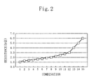
- Figure 2 illustrates respective resistance values R A of the regulating resistor network 16A corresponding to the individual combinations shown in Table 1, where the resistance values R 1 , R 2 , R 3 and R 4 of the first, second, third and fourth thin-film resistors 16a , 16b , 16c and 16d are 3, 4, 5 and 6 k ⁇ , respectively.
- an associated combination formed by cutting at least one of the first through fourth thin-film resistors 16a through 16d is known from Figure 2 and Table 1.
- the thin-film resistor(s) to be removed are cut off by being irradiated with laser light such as YAG laser radiation.
- YAG laser radiation is used for cutting the thin-film resistors off, then the thin-film resistors are cuttable quickly and yet the semiconductor substrate 10 receives little damage. This is because YAG laser radiation is well absorbable into the metal thin film as a material for the thin-film resistors, but hardly absorbable into the semiconductor substrate 10 of GaAs, for example.
- the semiconductor substrate 10 receives even smaller damage, because the laser irradiation time is very short in such a case.
- Figure 3(a) illustrates an overall arrangement of a semiconductor device according to the second embodiment
- Figure 3(b) illustrates a planar layout of a regulating resistor network 16B for the semiconductor device according to the second embodiment
- the second embodiment is the same as the first embodiment except that the regulating resistor network 16B of the second embodiment has a different Construction from that of the resistor network 16A of the first embodiment.
- the same components as those used in the first embodiment will be identified by the same reference numerals, and the description thereof will be omitted herein.
- the regulating resistor network 16B consists of first, second, third, fourth and fifth thin-film resistors 16a , 16b , 16c , 16d and 16e , which are connected in parallel to each other between the gate voltage supply terminal 15 and the ground terminal 17 .
- the first through fifth thin-film resistors 16a through 16e are formed out of a metal thin film of WSiN, for example, to have mutually different lengths.
- Each of the first through fourth thin-film resistors 16a through 16d is cuttable in 10 plus nanoseconds by being irradiated with laser light such as YAG laser radiation.
- the fifth thin-film resistor 16e has a resistance value larger than those of the first through fourth thin-film resistors 16a through 16d and is noncuttable by the laser light.
- the number of combinations formed by cutting at least one of the thin-film resistors is 16 in this embodiment.
- Figure 4 illustrates respective resistance values R B of the regulating resistor network 16B corresponding to the individual combinations shown in Table 1, where the resistance values R 1 , R 2 , R 3 , R 4 and R 5 of the first through fifth thin-film resistors 16a , 16b , 16c , 16d and 16e are 3, 4, 5, 6 and 7 k ⁇ , respectively.
- the resistance values R A of the regulating resistor network 16A according to the first embodiment are represented by the broken-line curve
- the resistance values R B of the regulating resistor network 16B according to the second embodiment are represented by the solid-line curve.
- the variation in resistance of the regulating resistor network 16B according to the second embodiment is gentler than that of the regulating resistor network 16A according to the first embodiment.
- a difference between resistance values associated with a pair of adjacent combinations can be reduced according to the second embodiment.
- the regulating resistor network 16B additionally includes the non-cuttable fifth thin-film resistor 16e .
- the regulating resistor network 16B is particularly effective if a difference between resistance values associated with a pair of adjacent combinations formed by cutting off a large number of thin-film resistors is much larger than a difference between resistance values associated with another pair of adjacent combinations formed by cutting off a small number of thin-film resistors.
- the thin-film resistors included in the regulating resistor network 16A or 16B at mutually different values, at least one of the material, cross-sectional area and length should be changed for the respective thin-film resistors. If these thin-film resistors are formed during the same process, however, all of these thin-film resistors should be made of the same material to an equal thickness. Accordingly, the thin-film resistors should have mutually different lengths or widths to make the resistance values thereof different from each other.
- the thin-film resistors included in the regulating resistor network 16A or 16B according to the first or second embodiment may be formed by a known technique. Specifically, first, a metal thin film is deposited over the entire surface of the semiconductor substrate 10 . Next, a resist pattern is defined by photolithography on the metal thin film. And then the metal thin film is patterned using the resist pattern as a mask.
- the feature size of the resist pattern formed by photolithography has a tolerance of about ⁇ 0.1/ ⁇ m from its desired value.
- each thin-film resistor reduces its width by about 0.2 ⁇ m in total due to unintentional side etching. Accordingly, in the worst-case scenario, the width of a thin-film resistor formed by patterning the metal thin film with a thickness of 0.1 ⁇ m may be smaller than its desired value by as much as about 0.3/ ⁇ m. It should be noted that neither an error resulting from photolithography or an error caused by side etching depends on the width of the thin-film resistor.
- Figure 5 illustrates a resistance adjustment circuit.
- the voltage divider 14 (with a resistance value R 0 ) and a regulating resistor network 16C (with a resistance value R c ) are connected in series to the voltage supply terminal 13 .
- the regulating resistor network 16C consists of first and second thin-film resistors 16a and 16b connected in parallel to each other.
- the resistance values of the voltage divider 14 and the first and second thin-film resistors 16a and 16b are preset at 4, 1 and 2 k ⁇ , respectively, in the resistance adjustment circuit shown in Figure 5 .
- the resistance values of the voltage divider 14 and the first and second thin-film resistors 16a and 16b are made different from each other by differentiating the widths of these resistors while equalizing their lengths with each other.
- the width ratio among the voltage divider 14 and the first and second thin-film resistors 16a and 16b may be set at 1:4:2.
- the widths of the voltage divider 14 and the first and second thin-film resistors 16a and 16b have decreased from their preset values, e.g., 1, 4 and 2 ⁇ m, by 0.3 ⁇ m each (i.e., their widths are now 0.7, 3.7 and 1.7 ⁇ m).
- the resistance values of the voltage divider 14 and the first through fifth thin-film resistors 16a through 16e are made different from each other by differentiating their lengths while equalizing their widths with each other, then these resistance values and the resistance division ratio of the resistance adjustment circuit are not affected by the error resulting from lithography and etching process steps.
- the voltage divider 14 and the first through fifth thin-film resistors 16a through 16e are made of the same metal thin film, then their thicknesses increase or decrease at the same ratio even if the thickness of the metal thin film deposited has deviated from its preset value. Thus, the resistance division ratio of the resistance adjustment circuit is not affected.
- the voltage divider 14 and the first through fifth thin-film resistors 16a through 16e are made of the same metal thin film, then their resistance values increase or decrease at the same ratio with a temperature variation. Thus, the resistance division ratio of the resistance adjustment circuit is not affected, either.
- a metal thin film is deposited over the entire surface of the semiconductor substrate 10 .
- a resist pattern is defined by photolithography on the metal thin film.
- the metal thin film is patterned using the resist pattern as a mask, thereby forming the regulating resistor network 16A or 16B according to the first or second embodiment.
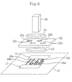
- Figure 6 illustrates an overall arrangement of an optical system for fusing and cutting off the first, second, third and/or fourth thin-film resistors 16a through 16d .
- the optical system includes: a laser light source 20 ; a first optical lens 21 ; a mask 22 ; and a second optical lens 23 .
- the light source 20 emits YAG laser radiation in pulses.
- the first optical lens 21 magnifies the irradiation area of the laser light emitted from the laser light source 20 .
- the mask 22 selectively transmits the light passed through the first optical lens 21 .
- the second optical lens 23 converges the light, which has been transmitted through the mask 22 , onto a target spot on the semiconductor substrate 10 .
- the mask 22 is provided with first, second, third and fourth openings 22a , 22b , 22c and 22d at respective locations corresponding to the cut portions of the first, second, third and fourth thin-film resistors 16a , 16b , 16c and 16d .
- the laser beams passed through the first through fourth openings 22a through 22d are imaged by the second optical lens 23 at the respective cut portions of the first through fourth thinfilm resistors 16a through 16d .
- imaging relationship is established by the second optical lens 23 between the first through fourth openings 22a through 22d of the mask 22 and the first through fourth thin-film resistors 16a through 16d .
- the rectangular frames drawn over the first through fourth thin-film resistors 16a through 16d represent the spots of beams converged by the second optical lens 23 .
- the laser light emitted from the laser light source 20 gets the irradiation area thereof magnified by the first optical lens 21 , only the central portion of the laser emission is transmitted through the first through fourth openings 22a through 22d of the mask 22 .
- the intensity distribution of the optical energy transmitted through the first through fourth openings 22a through 22d is substantially uniform.
- the first through fourth thin-film resistors 16a through 16d can be cut almost equally.
- the beams transmitted through the first through fourth openings 22a through 22d of the mask 22 are converged by the second optical lens 23 , high energy is applicable to the respective cut portions of the first through fourth thin-film resistors 16a through 16d .
- Figure 7 illustrates an overall arrangement of a resistance adjustment system for adjusting the resistance value of the regulating resistor network 16A or 16B by cutting off at least one of the first through fourth thin-film resistors 16a through 16d .
- the same optical system as that shown in Figure 6 is incorporated into this resistance adjustment system.
- the same component will be identified by the same reference numerals and the description thereof will be omitted herein.
- a horizontal stage 24 which is movable horizontally, is provided under the optical system.
- a semiconductor wafer 25 mounting the semiconductor substrate 10 thereon, is placed on the horizontal stage 24 .
- a plurality of probe needles 26a of a measuring unit 26 for measuring the operating current of the FET formed on the semiconductor substrate 10 are in contact with the semiconductor substrate 10 .
- the operating current values measured by the measuring unit 26 are provided to a controller 27 for controlling the opened/closed states of the first through fourth openings 22a through 22d of the mask 22 .
- light blocking plates 28 are placed beside the first through fourth openings 22a through 22d of the mask 22 and coupled to respective drivers 29 implemented as piezoelectric devices.
- the controller 27 determines through computations which of the first through fourth thin-film resistors 16a through 16d on the semiconductor substrate 10 should be cut off to minimize the difference between the actual operating current of the FET and the preset value thereof. And based on the results of computations, the controller 27 determines whether each of the first through fourth openings 22a through 22d of the mask 22 should be opened or closed, thereby instructing the drivers 29 to drive the light-blocking plates 28 as such.
- Step S1 the operating current of the FET is measured for the first time. Specifically, one of the probe needles 26a of the measuring unit 26 makes contact with the gate terminal of the FET, while two other probe needles 26a make contact with the drain and source terminals of the FET. In such a state, the current flowing between the drain and source terminals of the FET is measured with a variable gate voltage applied to the gate terminal of the FET.
- Step S2 it is determined for the first time based on the operating characteristic value of the FET whether the FET is GO or NO-GO. More specifically, it is determined whether or not the operating current measured by the measuring unit 26 is within a prescribed range.
- the "prescribed range” means a range in which the FET is qualified for a GO product if the resistance value of the regulating resistor network 16A or 16B in the resistance adjustment circuit connected to the gate terminal is adjusted.
- Step S3 the gate voltage to be applied to the gate terminal of the FET is derived in Step S3 .
- various gate voltages which are associated with the respective resistance values of the regulating resistor network 16A or 16B shown in Figure 2 or 4 , are applied to the gate terminal, thereby measuring the resulting operating current values of the FET.
- a gate voltage associated with an operating current closest to the desired operating current i.e., a predetermined optimum operating current
- Step S4 it is determined which of the first through fourth thin-film resistors should be cut off to apply the gate voltage derived in Step S3 to the gate terminal of the FET.
- Step S5 the selected thin-film resistor is cut off.
- the controller 27 determines whether each of the first through fourth openings 22a through 22d of the mask 22 should be opened or closed and instructs the drivers 29 to drive the light-blocking plates 28 as determined. And the laser light source 20 is driven to emit laser radiation toward the mask 22 , thereby cutting the selected thin-film resistor off.
- Step S6 the operating current of the FET is measured for the second time. Then, in Step S7 , it is determined for the second time based on the re-measured operating current value of the FET whether the FET is GO or NO-GO.
- Step S8 the horizontal stage is moved in Step S8 , and then the procedure returns to Step S1 to start to test another FET formed on another semiconductor substrate.
- Step S2 if the FET is evaluated as exhibiting "NO-GO" operating characteristic in Step S2 or S7 , then the semiconductor substrate 10 including such a defective FET is marked with ink, for example, in Step S9 . Thereafter, the horizontal stage is moved in Step S8 , and then the procedure returns to Step S1 to start to test another FET toned on another semiconductor substrate.
- measurement of the operating current of the FET on the semiconductor substrate 10 , GO/NO-GO test of the FET and resistance adjustment of the regulating resistor network 16A or 16B in the resistance adjustment circuit can be all performed at a wafer level (i.e., in the state where the semiconductor substrate 10 is still included in the semiconductor water 25 ).
- the time taken to adjust the resistance value of the resistance adjustment circuit can be shortened.
- the semiconductor circuit formed on the semiconductor substrate is supposed to be an FET.
- the semiconductor circuit may be an operational amplifier used for the inverting amplifier shown in Figure 9 .
- the regulating resistor may be a first resistor connected to the signal input terminal of the operational amplifier or a second resistor connected to the feedback loop of the operational amplifier.
- a first resistor 33 is connected between an operational amplifier 30 and a signal input terminal 31
- a second resistor 34 is connected to a feedback loop from a signal output terminal 32 to the operational amplifier 30 .
- the regulating resistor network 16A or 16B according to the first or second embodiment is applicable to at least one of the first and second resistors 33 and 34 .
- the regulating resistor network 16A or 16B is applicable to the first resistor 33 .
- the resistance value R P of the first resistor 33 increases, thus decreasing the gain A of the operational amplifier 30 .
- the regulating resistor network 16A or 16B is also applicable to the second resistor 34 .
- the resistance value R Q of the second resistor 34 increases, thus increasing the gain A of the operational amplifier 30 .
- the gain of the operational amplifier 30 for the inverting amplifier shown in Figure 9 may be measured and at least one of the first through fourth thin-film resistors 16a through 16d of the regulating resistor network 16A or 16B for the first or second resistor 33 or 34 may be cut off based on the gain measured. In this manner, the gain of the amplifier can be optimized for an electronic circuit.
Landscapes
- Engineering & Computer Science (AREA)
- Manufacturing & Machinery (AREA)
- Microelectronics & Electronic Packaging (AREA)
- Physics & Mathematics (AREA)
- Optics & Photonics (AREA)
- Plasma & Fusion (AREA)
- Semiconductor Integrated Circuits (AREA)
- Apparatuses And Processes For Manufacturing Resistors (AREA)
- Design And Manufacture Of Integrated Circuits (AREA)
- Laser Beam Processing (AREA)
- Non-Adjustable Resistors (AREA)
Applications Claiming Priority (2)
| Application Number | Priority Date | Filing Date | Title |
|---|---|---|---|
| JP31587398 | 1998-11-06 | ||
| JP31587398 | 1998-11-06 |
Publications (3)
| Publication Number | Publication Date |
|---|---|
| EP1003217A2 true EP1003217A2 (fr) | 2000-05-24 |
| EP1003217A3 EP1003217A3 (fr) | 2001-03-14 |
| EP1003217B1 EP1003217B1 (fr) | 2009-01-14 |
Family
ID=18070631
Family Applications (1)
| Application Number | Title | Priority Date | Filing Date |
|---|---|---|---|
| EP99122167A Expired - Lifetime EP1003217B1 (fr) | 1998-11-06 | 1999-11-05 | Réseau de résistances régulé, dispositif semi-conducteur comprenant ce réseau de résistance, et méthode de fabrication |
Country Status (9)
| Country | Link |
|---|---|
| US (2) | US6201288B1 (fr) |
| EP (1) | EP1003217B1 (fr) |
| JP (1) | JP3285021B2 (fr) |
| KR (1) | KR100662162B1 (fr) |
| CN (1) | CN1253363A (fr) |
| AU (1) | AU5823999A (fr) |
| CA (1) | CA2287791A1 (fr) |
| DE (1) | DE69940295D1 (fr) |
| TW (1) | TW429382B (fr) |
Cited By (2)
| Publication number | Priority date | Publication date | Assignee | Title |
|---|---|---|---|---|
| RU2361317C1 (ru) * | 2007-12-25 | 2009-07-10 | ОАО "Электровыпрямитель" | Способ изготовления резистивных элементов полупроводниковых резисторов |
| WO2013057689A1 (fr) | 2011-10-21 | 2013-04-25 | Ecole Polytechnique Federale De Lausanne (Epfl) | Transducteur de pression haute température sic |
Families Citing this family (18)
| Publication number | Priority date | Publication date | Assignee | Title |
|---|---|---|---|---|
| US6664500B2 (en) * | 2000-12-16 | 2003-12-16 | Anadigics, Inc. | Laser-trimmable digital resistor |
| JP2002334978A (ja) * | 2001-05-10 | 2002-11-22 | Sony Corp | 素子集積回路 |
| KR20050026904A (ko) * | 2001-09-10 | 2005-03-16 | 마이크로브리지 테크놀로지스 인크. | 저항기 트리밍 방법 |
| US6834065B2 (en) * | 2002-05-21 | 2004-12-21 | Carrier Access Corporation | Methods and apparatuses for direct digital drive of a laser in a passive optical network |
| DE10224180B4 (de) * | 2002-05-31 | 2007-01-04 | Infineon Technologies Ag | Schaltungsanordnung zur Einstellung des Eingangswiderstandes und der Eingangskapazität eines integrierten Halbleiterschaltungschips |
| AU2005203550A1 (en) * | 2004-08-23 | 2006-03-09 | Furukawa Co., Ltd. | Laser apparatus |
| US20060140233A1 (en) * | 2004-12-28 | 2006-06-29 | Jesse Chin | Laser driver with integrated bond options for selectable currents |
| JP2006332175A (ja) * | 2005-05-24 | 2006-12-07 | Freescale Semiconductor Inc | トリミング回路及び電子回路 |
| WO2007018171A1 (fr) * | 2005-08-05 | 2007-02-15 | Tti Ellebeau, Inc. | Dispositif d'iontophorese |
| KR20080047600A (ko) * | 2005-09-15 | 2008-05-29 | 티티아이 엘뷰 가부시키가이샤 | 로드형 이온토포레시스 장치 |
| US20070078445A1 (en) * | 2005-09-30 | 2007-04-05 | Curt Malloy | Synchronization apparatus and method for iontophoresis device to deliver active agents to biological interfaces |
| US20070078376A1 (en) * | 2005-09-30 | 2007-04-05 | Smith Gregory A | Functionalized microneedles transdermal drug delivery systems, devices, and methods |
| JP2007103775A (ja) | 2005-10-06 | 2007-04-19 | Matsushita Electric Ind Co Ltd | 可変抵抗器 |
| EP1965858A2 (fr) * | 2005-12-30 | 2008-09-10 | Tti Ellebeau, Inc. | Système et procédé de commande à distance d'un dispositif d'iontophorèse |
| CN101528300A (zh) * | 2006-09-05 | 2009-09-09 | Tti优而美株式会社 | 使用感应电源的透皮药物输送系统、装置和方法 |
| KR20090106492A (ko) | 2006-12-01 | 2009-10-09 | 티티아이 엘뷰 가부시키가이샤 | 경피성 전달 장치와 같은 장치에 전력을 제공하거나 제어하기 위한 시스템, 장치, 및 방법 |
| DE112011105993T5 (de) | 2011-12-23 | 2014-09-04 | Intel Corporation | Prozessabstimmbarer Widerstand mit Nutzerwählbaren Werten |
| CN114300535B (zh) * | 2021-12-30 | 2025-06-20 | 北海惠科半导体科技有限公司 | 数字晶体管的制作方法、数字晶体管及计算机可读存储介质 |
Family Cites Families (16)
| Publication number | Priority date | Publication date | Assignee | Title |
|---|---|---|---|---|
| US3699649A (en) * | 1969-11-05 | 1972-10-24 | Donald A Mcwilliams | Method of and apparatus for regulating the resistance of film resistors |
| US3758745A (en) * | 1971-09-07 | 1973-09-11 | Microsystems Int Ltd | Substrate positioned determination structure and method |
| DE3071642D1 (en) * | 1979-12-19 | 1986-07-24 | Seiko Epson Corp | A voltage regulator for a liquid crystal display |
| US4782320A (en) * | 1986-11-03 | 1988-11-01 | Vtc Incorporated | Mesh network for laser-trimmed integrated circuit resistors |
| JPS63140558A (ja) * | 1986-12-02 | 1988-06-13 | Toshiba Corp | 厚膜回路基板 |
| JPH01184861A (ja) * | 1988-01-13 | 1989-07-24 | Toshiba Corp | レーザ光によるトリミング方法 |
| JPH02174414A (ja) * | 1988-12-27 | 1990-07-05 | Hitachi Ltd | 半導体集積回路装置 |
| US5284794A (en) | 1990-02-21 | 1994-02-08 | Nippondenso Co., Ltd. | Method of making semiconductor device using a trimmable thin-film resistor |
| JP2664793B2 (ja) * | 1990-04-06 | 1997-10-22 | 株式会社東芝 | 半導体装置の製造方法 |
| IL94340A (en) * | 1990-05-09 | 1994-05-30 | Vishay Israel Ltd | Selectable high precision resistor and technique for production thereof |
| JP2938143B2 (ja) * | 1990-05-29 | 1999-08-23 | 沖電気工業株式会社 | 定着装置の製造方法 |
| JPH04209501A (ja) * | 1990-12-04 | 1992-07-30 | Mitsubishi Electric Corp | 半導体装置用基板 |
| US5243319A (en) * | 1991-10-30 | 1993-09-07 | Analog Devices, Inc. | Trimmable resistor network providing wide-range trims |
| JP3233492B2 (ja) * | 1993-04-21 | 2001-11-26 | 松下電子工業株式会社 | 半導体集積回路素子とそのバイアス調整方法 |
| JP3570086B2 (ja) * | 1996-06-11 | 2004-09-29 | ミツミ電機株式会社 | 抵抗回路及びその調整方法 |
| US6326256B1 (en) * | 1998-12-18 | 2001-12-04 | Texas Instruments Incorporated | Method of producing a laser trimmable thin film resistor in an integrated circuit |
-
1999
- 1999-10-26 TW TW088118476A patent/TW429382B/zh not_active IP Right Cessation
- 1999-10-29 CA CA002287791A patent/CA2287791A1/fr not_active Abandoned
- 1999-11-02 US US09/432,107 patent/US6201288B1/en not_active Expired - Fee Related
- 1999-11-03 AU AU58239/99A patent/AU5823999A/en not_active Abandoned
- 1999-11-04 CN CN99122373A patent/CN1253363A/zh active Pending
- 1999-11-04 JP JP31342499A patent/JP3285021B2/ja not_active Expired - Fee Related
- 1999-11-04 KR KR1019990048476A patent/KR100662162B1/ko not_active Expired - Fee Related
- 1999-11-05 DE DE69940295T patent/DE69940295D1/de not_active Expired - Lifetime
- 1999-11-05 EP EP99122167A patent/EP1003217B1/fr not_active Expired - Lifetime
-
2001
- 2001-01-05 US US09/754,308 patent/US6649463B2/en not_active Expired - Fee Related
Cited By (2)
| Publication number | Priority date | Publication date | Assignee | Title |
|---|---|---|---|---|
| RU2361317C1 (ru) * | 2007-12-25 | 2009-07-10 | ОАО "Электровыпрямитель" | Способ изготовления резистивных элементов полупроводниковых резисторов |
| WO2013057689A1 (fr) | 2011-10-21 | 2013-04-25 | Ecole Polytechnique Federale De Lausanne (Epfl) | Transducteur de pression haute température sic |
Also Published As
| Publication number | Publication date |
|---|---|
| KR20000035213A (ko) | 2000-06-26 |
| JP2000200876A (ja) | 2000-07-18 |
| KR100662162B1 (ko) | 2006-12-27 |
| TW429382B (en) | 2001-04-11 |
| CA2287791A1 (fr) | 2000-05-06 |
| JP3285021B2 (ja) | 2002-05-27 |
| US6201288B1 (en) | 2001-03-13 |
| CN1253363A (zh) | 2000-05-17 |
| US6649463B2 (en) | 2003-11-18 |
| AU5823999A (en) | 2000-05-11 |
| US20010001493A1 (en) | 2001-05-24 |
| EP1003217B1 (fr) | 2009-01-14 |
| EP1003217A3 (fr) | 2001-03-14 |
| DE69940295D1 (de) | 2009-03-05 |
Similar Documents
| Publication | Publication Date | Title |
|---|---|---|
| US6201288B1 (en) | Regulating resistor network, semiconductor device including the resistor network, and method for fabricating the device | |
| TWI858556B (zh) | 用於在單一微影曝光遍次中形成多個空間影像之光產生系統及控制系統 | |
| DE69625093T2 (de) | Belichtungsverfahren, Belichtungsapparat und Verfahren zur Herstellung einer Vorrichtung | |
| KR100916281B1 (ko) | 미세구조의 임의 배치를 통하여 다결정성 박막 트랜지스터균일성을 향상시키는 방법 | |
| JP3325350B2 (ja) | レーザ露光装置及び半導体装置の製造方法 | |
| DE102013009419A1 (de) | Laserausheil- bzw. -annealingsysteme und Verfahren mit ultrakurzen Verweil- bzw. Haltezeiten | |
| JP4127664B2 (ja) | 現像処理装置の調整方法 | |
| US20050270613A1 (en) | System and method for dose control in a lithographic system | |
| US20040130436A1 (en) | Laser-trimmable digital resistor | |
| US20070185606A1 (en) | Exposure apparatus and device manufacturing method | |
| US4241315A (en) | Adjustable current source | |
| JP4245294B2 (ja) | 半導体集積デバイスのインピーダンスをチューニングする方法および装置 | |
| US7033903B2 (en) | Method and apparatus for forming patterned photoresist layer | |
| US20060204859A1 (en) | An extra dose trim mask, method of manufacture, and lithographic process using the same | |
| US6809801B2 (en) | 1:1 projection system and method for laser irradiating semiconductor films | |
| KR100668185B1 (ko) | 박막 칩 저항기 제조방법 | |
| Wagner | Functional laser trimming: An overview | |
| US6482573B1 (en) | Exposure correction based on reflective index for photolithographic process control | |
| JPH07131026A (ja) | 薄膜半導体装置およびその製造方法 | |
| US7642845B2 (en) | Circuit for creating tracking transconductors of different types | |
| GB2230625A (en) | Voltage regulator | |
| CN112394546B (zh) | 行波电极调制器集成端接电阻的调控方法及系统 | |
| JP3641348B2 (ja) | 半導体装置の製法 | |
| Meunier et al. | Novel laser trimming technique for microelectronics | |
| JP2002176103A (ja) | 半導体装置およびその製造方法 |
Legal Events
| Date | Code | Title | Description |
|---|---|---|---|
| PUAI | Public reference made under article 153(3) epc to a published international application that has entered the european phase |
Free format text: ORIGINAL CODE: 0009012 |
|
| AK | Designated contracting states |
Kind code of ref document: A2 Designated state(s): DE FR GB |
|
| AX | Request for extension of the european patent |
Free format text: AL;LT;LV;MK;RO;SI |
|
| PUAL | Search report despatched |
Free format text: ORIGINAL CODE: 0009013 |
|
| AK | Designated contracting states |
Kind code of ref document: A3 Designated state(s): AT BE CH CY DE DK ES FI FR GB GR IE IT LI LU MC NL PT SE |
|
| AX | Request for extension of the european patent |
Free format text: AL;LT;LV;MK;RO;SI |
|
| RIC1 | Information provided on ipc code assigned before grant |
Free format text: 7H 01L 27/06 A, 7H 01C 17/242 B, 7H 01L 27/08 B |
|
| 17P | Request for examination filed |
Effective date: 20010628 |
|
| AKX | Designation fees paid |
Free format text: DE FR GB |
|
| 17Q | First examination report despatched |
Effective date: 20070118 |
|
| GRAP | Despatch of communication of intention to grant a patent |
Free format text: ORIGINAL CODE: EPIDOSNIGR1 |
|
| GRAS | Grant fee paid |
Free format text: ORIGINAL CODE: EPIDOSNIGR3 |
|
| RAP1 | Party data changed (applicant data changed or rights of an application transferred) |
Owner name: PANASONIC CORPORATION |
|
| GRAA | (expected) grant |
Free format text: ORIGINAL CODE: 0009210 |
|
| AK | Designated contracting states |
Kind code of ref document: B1 Designated state(s): DE FR GB |
|
| REG | Reference to a national code |
Ref country code: GB Ref legal event code: FG4D |
|
| REF | Corresponds to: |
Ref document number: 69940295 Country of ref document: DE Date of ref document: 20090305 Kind code of ref document: P |
|
| PLBE | No opposition filed within time limit |
Free format text: ORIGINAL CODE: 0009261 |
|
| STAA | Information on the status of an ep patent application or granted ep patent |
Free format text: STATUS: NO OPPOSITION FILED WITHIN TIME LIMIT |
|
| 26N | No opposition filed |
Effective date: 20091015 |
|
| PGFP | Annual fee paid to national office [announced via postgrant information from national office to epo] |
Ref country code: DE Payment date: 20091029 Year of fee payment: 11 |
|
| PGFP | Annual fee paid to national office [announced via postgrant information from national office to epo] |
Ref country code: GB Payment date: 20091104 Year of fee payment: 11 Ref country code: FR Payment date: 20091123 Year of fee payment: 11 |
|
| GBPC | Gb: european patent ceased through non-payment of renewal fee |
Effective date: 20101105 |
|
| REG | Reference to a national code |
Ref country code: FR Ref legal event code: ST Effective date: 20110801 |
|
| REG | Reference to a national code |
Ref country code: DE Ref legal event code: R119 Ref document number: 69940295 Country of ref document: DE Effective date: 20110601 Ref country code: DE Ref legal event code: R119 Ref document number: 69940295 Country of ref document: DE Effective date: 20110531 |
|
| PG25 | Lapsed in a contracting state [announced via postgrant information from national office to epo] |
Ref country code: DE Free format text: LAPSE BECAUSE OF NON-PAYMENT OF DUE FEES Effective date: 20110531 |
|
| PG25 | Lapsed in a contracting state [announced via postgrant information from national office to epo] |
Ref country code: FR Free format text: LAPSE BECAUSE OF NON-PAYMENT OF DUE FEES Effective date: 20101130 |
|
| PG25 | Lapsed in a contracting state [announced via postgrant information from national office to epo] |
Ref country code: GB Free format text: LAPSE BECAUSE OF NON-PAYMENT OF DUE FEES Effective date: 20101105 |