EP1003272A2 - Circuit de commutation - Google Patents
Circuit de commutation Download PDFInfo
- Publication number
- EP1003272A2 EP1003272A2 EP99308724A EP99308724A EP1003272A2 EP 1003272 A2 EP1003272 A2 EP 1003272A2 EP 99308724 A EP99308724 A EP 99308724A EP 99308724 A EP99308724 A EP 99308724A EP 1003272 A2 EP1003272 A2 EP 1003272A2
- Authority
- EP
- European Patent Office
- Prior art keywords
- condenser
- parallel
- transistor
- switching element
- circuit
- Prior art date
- Legal status (The legal status is an assumption and is not a legal conclusion. Google has not performed a legal analysis and makes no representation as to the accuracy of the status listed.)
- Withdrawn
Links
Images



Classifications
-
- H—ELECTRICITY
- H02—GENERATION; CONVERSION OR DISTRIBUTION OF ELECTRIC POWER
- H02M—APPARATUS FOR CONVERSION BETWEEN AC AND AC, BETWEEN AC AND DC, OR BETWEEN DC AND DC, AND FOR USE WITH MAINS OR SIMILAR POWER SUPPLY SYSTEMS; CONVERSION OF DC OR AC INPUT POWER INTO SURGE OUTPUT POWER; CONTROL OR REGULATION THEREOF
- H02M3/00—Conversion of DC power input into DC power output
- H02M3/02—Conversion of DC power input into DC power output without intermediate conversion into AC
- H02M3/04—Conversion of DC power input into DC power output without intermediate conversion into AC by static converters
- H02M3/10—Conversion of DC power input into DC power output without intermediate conversion into AC by static converters using discharge tubes with control electrode or semiconductor devices with control electrode
-
- H—ELECTRICITY
- H10—SEMICONDUCTOR DEVICES; ELECTRIC SOLID-STATE DEVICES NOT OTHERWISE PROVIDED FOR
- H10D—INORGANIC ELECTRIC SEMICONDUCTOR DEVICES
- H10D84/00—Integrated devices formed in or on semiconductor substrates that comprise only semiconducting layers, e.g. on Si wafers or on GaAs-on-Si wafers
- H10D84/101—Integrated devices comprising main components and built-in components, e.g. IGBT having built-in freewheel diode
- H10D84/141—VDMOS having built-in components
- H10D84/143—VDMOS having built-in components the built-in components being PN junction diodes
- H10D84/144—VDMOS having built-in components the built-in components being PN junction diodes in antiparallel diode configurations
-
- H—ELECTRICITY
- H10—SEMICONDUCTOR DEVICES; ELECTRIC SOLID-STATE DEVICES NOT OTHERWISE PROVIDED FOR
- H10D—INORGANIC ELECTRIC SEMICONDUCTOR DEVICES
- H10D30/00—Field-effect transistors [FET]
- H10D30/60—Insulated-gate field-effect transistors [IGFET]
- H10D30/64—Double-diffused metal-oxide semiconductor [DMOS] FETs
- H10D30/66—Vertical DMOS [VDMOS] FETs
-
- H—ELECTRICITY
- H10—SEMICONDUCTOR DEVICES; ELECTRIC SOLID-STATE DEVICES NOT OTHERWISE PROVIDED FOR
- H10D—INORGANIC ELECTRIC SEMICONDUCTOR DEVICES
- H10D62/00—Semiconductor bodies, or regions thereof, of devices having potential barriers
- H10D62/10—Shapes, relative sizes or dispositions of the regions of the semiconductor bodies; Shapes of the semiconductor bodies
- H10D62/102—Constructional design considerations for preventing surface leakage or controlling electric field concentration
- H10D62/103—Constructional design considerations for preventing surface leakage or controlling electric field concentration for increasing or controlling the breakdown voltage of reverse-biased devices
- H10D62/105—Constructional design considerations for preventing surface leakage or controlling electric field concentration for increasing or controlling the breakdown voltage of reverse-biased devices by having particular doping profiles, shapes or arrangements of PN junctions; by having supplementary regions, e.g. junction termination extension [JTE]
- H10D62/109—Reduced surface field [RESURF] PN junction structures
- H10D62/111—Multiple RESURF structures, e.g. double RESURF or 3D-RESURF structures
-
- H—ELECTRICITY
- H02—GENERATION; CONVERSION OR DISTRIBUTION OF ELECTRIC POWER
- H02M—APPARATUS FOR CONVERSION BETWEEN AC AND AC, BETWEEN AC AND DC, OR BETWEEN DC AND DC, AND FOR USE WITH MAINS OR SIMILAR POWER SUPPLY SYSTEMS; CONVERSION OF DC OR AC INPUT POWER INTO SURGE OUTPUT POWER; CONTROL OR REGULATION THEREOF
- H02M3/00—Conversion of DC power input into DC power output
- H02M3/003—Constructional details, e.g. physical layout, assembly, wiring or busbar connections
Definitions
- the present invention relates in general to a switching circuit. More specifically, the invention relates to a soft switching circuit that realizes the low noise and high efficiency of an electric-power converter.
- FIG 8 shows a voltage resonance circuit that is utilized in a television or other electrical equipment, in which Q1 denotes a metal oxide semiconductor field-effect transistor (MOSFET). More specifically, a primary winding N1 of a transformer Tr is connected to a DC power supply Vin via the transistor Q1. A diode D1 is connected in anti-parallel to the transistor Q1. A condenser Cs is connected in parallel to the transistor Q1. A condenser Co is connected to a primary winding N2 of the transformer Tr via a diode D2, wherein a load Ro is connected to the condenser Co. The diode D2 and the condenser Co form a rectifying and smoothing circuit. A parasitic diode of the transistor Q1 may be used as the diode D1.
- MOSFET metal oxide semiconductor field-effect transistor
- the electric charge stored in the condenser Cs is emitted by the following route: the condenser Cs, an excitation inductance of the transformer Tr, and the DC power supply Vin. Even if the voltage of the condenser Cs becomes 0V, the electric current of the excitation inductance of the transformer Tr flows into the DC power supply Vin through the diode D1.
- Transistor Q1 is turned on while the electric current is passed through the diode D1. Then, the excitation energy is stored again in the transformer Tr by the previously-described route: the DC power supply Vin, the primary winding N1 of the transformer, and the transistor Q1.
- the condenser Cs connected in parallel to transistor Q1 is charged from 0V while the transistor Q1 is off.
- ZVS zero voltage switching
- the ZVS is also performed while the transistor Q1 is on, since the transistor Q1 is turned on while the diode D1 connected in parallel to the transistor Q1 is conductive.
- the transistor Q1 is on.
- the energy stored in Cs is hardly lost because it is regenerated into the power supply when it is emitted by the following route: the condenser Cs, the excitation inductance of the transformer Tr, and the DC power supply Vin.
- the above-mentioned voltage resonance circuit with little switching loss and radiation noise is applicable for use in a television or other electronic devices.
- the resonance voltage of the resonance circuit formed by the excitation inductance of the transformer Tr and the condenser Cs, is applied to the transistor Q1.
- the MOSFET applied to the television or the like must have a breakdown voltage of the 1800V-class, although the DC voltage is about 120V.
- the increase in the ON-resistance of the MOSFET is proportional to the breakdown voltage to the power of 2.5.
- the MOSFET with the high breakdown voltage has such a disadvantage that there is a large conduction loss.
- the parallel condenser Cs with about several nF to several tens of nF must have a high voltage proof.
- the invention accomplishes the above object by providing a switching circuit in which a condenser is connected in parallel to a switching element to perform a resonance operation with an inductance, wherein a super-junction MOSFET is used as the switching element, and the MOSFET has a drift region that is composed of thin p-layers and n-layers alternately stacked or piled up.
- the output capacitance of the super-junction MOSFET may be used as the parallel condenser.
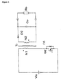
- Figure 1 is a circuit diagram showing a first embodiment of the present invention.
- the circuit illustrated in Figure 1 is different from that illustrated in Figure 8, in that the transistor Q1 is replaced with a transistor Q2, which is a super-junction MOSFET (hereinafter abbreviated as a SJMOSFET), and that the condenser Cs is eliminated.
- a SJMOSFET super-junction MOSFET
- the operation of the circuit in Figure 1 will not be described in great detail, since the description with reference to the operation of the circuit in Figure 8 is applicable, as would be readily understood by one of skill in the art, if the transistor Q1 is replaced with transistor Q2 and the condenser Cs is replaced with the output capacitance of transistor Q2.
- the ON resistance of a switching element is lowered to reduce the conduction loss and eliminate the necessity for the condenser Cs or reduce the capacitance of the condenser Cs.
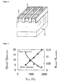
- Figure 3 shows the ON resistance ratio Ron(SJ)/Ron(CONV) and the charge ratio Qon(SJ)/Qon(CONV) at the time of the switching between the SJMOSFET and the conventional MOSFET. More specifically, the higher breakdown voltage of the SJMOSFET is, the smaller the ON resistance is and the larger the quantity of electric charge is compared with the conventional MOSFET. In the case of an element of the 1800V-class, the ON resistance is decreased to about 1/40 and the quantity of electric charge is increased 20 times.
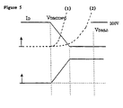
- Figure 4 shows the characteristics of the output capacitance Coss with respect to the applied voltage V DS .
- the output capacitance Coss is sharply decreased from approximately 10V [vid.(1)].
- the applied voltage V DS is sharply decreased from about 200V [vid. (2)].
- FIG. 6 shows an example of a partial resonance circuit in accordance with an embodiment of the invention.
- a series circuit composed of a primary winding N1 of a transformer Tr and a SJMOSFET Q3 is connected to a DC power supply Vin.
- a diode D3 is connected in anti-parallel to the transistor Q3.
- a condenser Cs is connected in parallel to the transistor Q3, a series circuit composed of a tertiary winding N3 of the transformer Tr, a diode D9 and transistor (MOSFET) Q4 is connected in parallel to transistor Q3.
- a rectifying and smoothing circuit composed of a diode D2 and a Condenser Co is connected to the secondary winding N2 of the transformer Tr.
- a load Ro is connected to the condenser Co.
- the parasitic diode of transistor Q3 may be used as the diode D3.
- the transistor Q4 is turned on to discharge the condenser Cs and the output capacitance of the transistor Q3, and then transistor Q3 is turned on under zero voltage.
- zero voltage switching ZVS is performed.
- the ZVS is also performed when transistor Q3 is turned off since the condenser Cs and the output capacitance of transistor Q3 are charged from 0V.
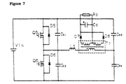
- Figure 7 shows an electric current resonance/voltage resonance circuit (a composite resonance circuit) in accordance with the invention.
- a series circuit composed of SJMOSFETs Q5 and Q6 to a DC power supply Vin.
- Diodes D5 and D6 are connected in anti-parallel to SJMOSFETs Q5 and Q6, respectively.
- Condensers Cs1 and Cs2 are connected in parallel to SJMOSFETs Q5 and Q6, respectively.
- a series circuit of condensers Cs3 and Cs4 is in parallel to the series circuit of Q5 and Q6.
- a primary winding of transformer Tr is connected via a reactor L1 between a middle point of the series circuit Q5, Q6 and a middle point of the series circuit Cs3, Cs4.
- the transformer has two secondary windings to which Diodes D7 and D8 are connected, so that a fullwave rectifying circuit is formed.
- a smoothing condenser Co is connected to the rectifying circuit; and a load Ro is connected to the condenser Co.
- the composite resonance circuit can also perform the ZVS (switching) operation by turning on transistors Q5 and Q6 alternately.
Landscapes
- Engineering & Computer Science (AREA)
- Power Engineering (AREA)
- Dc-Dc Converters (AREA)
- Inverter Devices (AREA)
- Electronic Switches (AREA)
Applications Claiming Priority (2)
| Application Number | Priority Date | Filing Date | Title |
|---|---|---|---|
| JP32658898 | 1998-11-17 | ||
| JP10326588A JP2000156978A (ja) | 1998-11-17 | 1998-11-17 | ソフトスイッチング回路 |
Publications (2)
| Publication Number | Publication Date |
|---|---|
| EP1003272A2 true EP1003272A2 (fr) | 2000-05-24 |
| EP1003272A3 EP1003272A3 (fr) | 2003-08-27 |
Family
ID=18189504
Family Applications (1)
| Application Number | Title | Priority Date | Filing Date |
|---|---|---|---|
| EP99308724A Withdrawn EP1003272A3 (fr) | 1998-11-17 | 1999-11-03 | Circuit de commutation |
Country Status (3)
| Country | Link |
|---|---|
| EP (1) | EP1003272A3 (fr) |
| JP (1) | JP2000156978A (fr) |
| KR (1) | KR20000035494A (fr) |
Cited By (4)
| Publication number | Priority date | Publication date | Assignee | Title |
|---|---|---|---|---|
| US6346464B1 (en) * | 1999-06-28 | 2002-02-12 | Kabushiki Kaisha Toshiba | Manufacturing method of semiconductor device |
| CN100588095C (zh) * | 2006-04-06 | 2010-02-03 | 株式会社日立制作所 | 单向dc-dc变换器 |
| US10243476B2 (en) | 2015-12-24 | 2019-03-26 | Kabushiki Kaisha Yaskawa Denki | Power conversion device and power conversion method |
| US11929682B2 (en) | 2022-04-26 | 2024-03-12 | Aes Global Holdings Pte Ltd. | ZVS assist snubber for switching converter |
Families Citing this family (37)
| Publication number | Priority date | Publication date | Assignee | Title |
|---|---|---|---|---|
| US6461918B1 (en) | 1999-12-20 | 2002-10-08 | Fairchild Semiconductor Corporation | Power MOS device with improved gate charge performance |
| JP4528460B2 (ja) * | 2000-06-30 | 2010-08-18 | 株式会社東芝 | 半導体素子 |
| US7745289B2 (en) | 2000-08-16 | 2010-06-29 | Fairchild Semiconductor Corporation | Method of forming a FET having ultra-low on-resistance and low gate charge |
| JP4764987B2 (ja) * | 2000-09-05 | 2011-09-07 | 富士電機株式会社 | 超接合半導体素子 |
| GB2373634B (en) * | 2000-10-31 | 2004-12-08 | Fuji Electric Co Ltd | Semiconductor device |
| US6916745B2 (en) | 2003-05-20 | 2005-07-12 | Fairchild Semiconductor Corporation | Structure and method for forming a trench MOSFET having self-aligned features |
| US6677641B2 (en) | 2001-10-17 | 2004-01-13 | Fairchild Semiconductor Corporation | Semiconductor structure with improved smaller forward voltage loss and higher blocking capability |
| US7345342B2 (en) | 2001-01-30 | 2008-03-18 | Fairchild Semiconductor Corporation | Power semiconductor devices and methods of manufacture |
| US6710403B2 (en) | 2002-07-30 | 2004-03-23 | Fairchild Semiconductor Corporation | Dual trench power MOSFET |
| US6803626B2 (en) | 2002-07-18 | 2004-10-12 | Fairchild Semiconductor Corporation | Vertical charge control semiconductor device |
| US6818513B2 (en) | 2001-01-30 | 2004-11-16 | Fairchild Semiconductor Corporation | Method of forming a field effect transistor having a lateral depletion structure |
| US6713813B2 (en) | 2001-01-30 | 2004-03-30 | Fairchild Semiconductor Corporation | Field effect transistor having a lateral depletion structure |
| US7132712B2 (en) | 2002-11-05 | 2006-11-07 | Fairchild Semiconductor Corporation | Trench structure having one or more diodes embedded therein adjacent a PN junction |
| US7061066B2 (en) | 2001-10-17 | 2006-06-13 | Fairchild Semiconductor Corporation | Schottky diode using charge balance structure |
| US7078296B2 (en) | 2002-01-16 | 2006-07-18 | Fairchild Semiconductor Corporation | Self-aligned trench MOSFETs and methods for making the same |
| KR100859701B1 (ko) | 2002-02-23 | 2008-09-23 | 페어차일드코리아반도체 주식회사 | 고전압 수평형 디모스 트랜지스터 및 그 제조 방법 |
| US7033891B2 (en) | 2002-10-03 | 2006-04-25 | Fairchild Semiconductor Corporation | Trench gate laterally diffused MOSFET devices and methods for making such devices |
| US7576388B1 (en) | 2002-10-03 | 2009-08-18 | Fairchild Semiconductor Corporation | Trench-gate LDMOS structures |
| US6710418B1 (en) | 2002-10-11 | 2004-03-23 | Fairchild Semiconductor Corporation | Schottky rectifier with insulation-filled trenches and method of forming the same |
| US7638841B2 (en) | 2003-05-20 | 2009-12-29 | Fairchild Semiconductor Corporation | Power semiconductor devices and methods of manufacture |
| KR100994719B1 (ko) | 2003-11-28 | 2010-11-16 | 페어차일드코리아반도체 주식회사 | 슈퍼정션 반도체장치 |
| US7368777B2 (en) | 2003-12-30 | 2008-05-06 | Fairchild Semiconductor Corporation | Accumulation device with charge balance structure and method of forming the same |
| US7352036B2 (en) | 2004-08-03 | 2008-04-01 | Fairchild Semiconductor Corporation | Semiconductor power device having a top-side drain using a sinker trench |
| US7265415B2 (en) | 2004-10-08 | 2007-09-04 | Fairchild Semiconductor Corporation | MOS-gated transistor with reduced miller capacitance |
| WO2006108011A2 (fr) | 2005-04-06 | 2006-10-12 | Fairchild Semiconductor Corporation | Transistors a effet de champ a grille en tranchees, et procedes de creation desdits transistors |
| US7385248B2 (en) | 2005-08-09 | 2008-06-10 | Fairchild Semiconductor Corporation | Shielded gate field effect transistor with improved inter-poly dielectric |
| US7446374B2 (en) | 2006-03-24 | 2008-11-04 | Fairchild Semiconductor Corporation | High density trench FET with integrated Schottky diode and method of manufacture |
| US7319256B1 (en) | 2006-06-19 | 2008-01-15 | Fairchild Semiconductor Corporation | Shielded gate trench FET with the shield and gate electrodes being connected together |
| CN101868856B (zh) | 2007-09-21 | 2014-03-12 | 飞兆半导体公司 | 用于功率器件的超结结构及制造方法 |
| US7772668B2 (en) | 2007-12-26 | 2010-08-10 | Fairchild Semiconductor Corporation | Shielded gate trench FET with multiple channels |
| US20120273916A1 (en) | 2011-04-27 | 2012-11-01 | Yedinak Joseph A | Superjunction Structures for Power Devices and Methods of Manufacture |
| US8319290B2 (en) | 2010-06-18 | 2012-11-27 | Fairchild Semiconductor Corporation | Trench MOS barrier schottky rectifier with a planar surface using CMP techniques |
| US8673700B2 (en) | 2011-04-27 | 2014-03-18 | Fairchild Semiconductor Corporation | Superjunction structures for power devices and methods of manufacture |
| US8772868B2 (en) | 2011-04-27 | 2014-07-08 | Fairchild Semiconductor Corporation | Superjunction structures for power devices and methods of manufacture |
| US8836028B2 (en) | 2011-04-27 | 2014-09-16 | Fairchild Semiconductor Corporation | Superjunction structures for power devices and methods of manufacture |
| US8786010B2 (en) | 2011-04-27 | 2014-07-22 | Fairchild Semiconductor Corporation | Superjunction structures for power devices and methods of manufacture |
| JP6179652B2 (ja) * | 2015-12-24 | 2017-08-16 | 株式会社安川電機 | 電力変換装置及び電力変換方法 |
Family Cites Families (2)
| Publication number | Priority date | Publication date | Assignee | Title |
|---|---|---|---|---|
| CN1019720B (zh) * | 1991-03-19 | 1992-12-30 | 电子科技大学 | 半导体功率器件 |
| JP3116338B2 (ja) * | 1994-03-22 | 2000-12-11 | 横河電機株式会社 | スイッチング電源 |
-
1998
- 1998-11-17 JP JP10326588A patent/JP2000156978A/ja active Pending
-
1999
- 1999-11-03 EP EP99308724A patent/EP1003272A3/fr not_active Withdrawn
- 1999-11-16 KR KR1019990050795A patent/KR20000035494A/ko not_active Ceased
Non-Patent Citations (2)
| Title |
|---|
| MURAKAMI N.; YAMASAKI M.: "Analysis of a resonant reset condition for a single-ended forward converter", PROCEEDINGS OF PESC'88, POWER ELECTRONICS SPECIALISTS CONFERENCE, 11 April 1998 (1998-04-11), pages 1018 - 1023 * |
| TATSUHIKO FUJIHIRA; YASUSHI MIYASAKA: "SIMULATED SUPERIOR PERFORMANCE OF SEMICONDUCTOR SUPERJUNCTION DEVICES", PROCEEDINGS OF 1998 INTERNATIONAL SYMPOSIUM ON POWER SEMICONDUCTOR SUPERJUNCTION DEVICES *A ICS, 3 June 1998 (1998-06-03) - 6 June 1998 (1998-06-06), KYOTO (JAPAN), pages 423 - 426 * |
Cited By (6)
| Publication number | Priority date | Publication date | Assignee | Title |
|---|---|---|---|---|
| US6346464B1 (en) * | 1999-06-28 | 2002-02-12 | Kabushiki Kaisha Toshiba | Manufacturing method of semiconductor device |
| USRE41181E1 (en) * | 1999-06-28 | 2010-03-30 | Kabushiki Kaisha Toshiba | Manufacturing method of semiconductor device |
| CN100588095C (zh) * | 2006-04-06 | 2010-02-03 | 株式会社日立制作所 | 单向dc-dc变换器 |
| US10243476B2 (en) | 2015-12-24 | 2019-03-26 | Kabushiki Kaisha Yaskawa Denki | Power conversion device and power conversion method |
| US11929682B2 (en) | 2022-04-26 | 2024-03-12 | Aes Global Holdings Pte Ltd. | ZVS assist snubber for switching converter |
| US12316227B2 (en) | 2022-04-26 | 2025-05-27 | Aes Global Holdings Pte Ltd. | ZVS assist snubber for switching converter |
Also Published As
| Publication number | Publication date |
|---|---|
| EP1003272A3 (fr) | 2003-08-27 |
| KR20000035494A (ko) | 2000-06-26 |
| JP2000156978A (ja) | 2000-06-06 |
Similar Documents
| Publication | Publication Date | Title |
|---|---|---|
| JP2000156978A (ja) | ソフトスイッチング回路 | |
| US6597590B2 (en) | 3-Level inverter apparatus | |
| US7321224B2 (en) | DC-DC converter with clamping capacitor and output winding for reduced output voltage ripple | |
| US10784859B2 (en) | Transformer based gate drive circuit | |
| EP1909381A1 (fr) | Convertisseur cc-cc | |
| US20010050549A1 (en) | Switch mode power supply with reduced switching losses | |
| US20050162139A1 (en) | Alternating current switching circuit | |
| US9130478B2 (en) | Rectifier with bridge circuit and parallel resonant circuit | |
| US10432081B2 (en) | Waveform shaping circuit, semiconductor device, and switching power supply device | |
| Kollman et al. | 10 MHz PWM Converters with GaAs VFETs | |
| EP1229635B1 (fr) | Circuit de verrouillage actif pour circuit redresseur synchrone autopiloté | |
| WO2014105313A1 (fr) | Alimentation électrique hors ligne à haute densité de puissance | |
| Slawinski et al. | System study of SiC MOSFET and Si IGBT power module performance using a bidirectional buck-boost converter as evaluation platform | |
| US20240195312A1 (en) | Synchronous rectifier circuit powered by a portion of secondary windings | |
| US6487094B1 (en) | High efficiency DC-DC power converter | |
| US6477064B1 (en) | High efficiency DC-DC power converter with turn-off snubber | |
| CN1054948C (zh) | 转换电源装置 | |
| JPH1169803A (ja) | スイッチング電源 | |
| US10498213B2 (en) | Drive circuit and semiconductor module utilizing a capacitance ratio between different switches | |
| Bisi et al. | 140-mOhm GaN Bidirectional Switch for Single-Stage Power Converters | |
| CN118199366A (zh) | 由次级绕组的一部分供电的同步整流器电路 | |
| JPH11187653A (ja) | 同期整流回路およびこの同期整流回路を用いたdc−dcコンバータ | |
| US11290100B2 (en) | Semiconductor device | |
| Nagao et al. | An E-mode p-GaN HEMT monolithically-integrated three-level gate driver operating with a single voltage supply | |
| JP2962388B2 (ja) | 二石式絶縁形スイッチング電源 |
Legal Events
| Date | Code | Title | Description |
|---|---|---|---|
| PUAI | Public reference made under article 153(3) epc to a published international application that has entered the european phase |
Free format text: ORIGINAL CODE: 0009012 |
|
| AK | Designated contracting states |
Kind code of ref document: A2 Designated state(s): AT BE CH CY DE DK ES FI FR GB GR IE IT LI LU MC NL PT SE |
|
| AX | Request for extension of the european patent |
Free format text: AL;LT;LV;MK;RO;SI |
|
| PUAL | Search report despatched |
Free format text: ORIGINAL CODE: 0009013 |
|
| AK | Designated contracting states |
Designated state(s): AT BE CH CY DE DK ES FI FR GB GR IE IT LI LU MC NL PT SE |
|
| AX | Request for extension of the european patent |
Extension state: AL LT LV MK RO SI |
|
| RIC1 | Information provided on ipc code assigned before grant |
Ipc: 7H 02M 3/335 B Ipc: 7H 02M 3/00 A |
|
| 17P | Request for examination filed |
Effective date: 20031006 |
|
| 17Q | First examination report despatched |
Effective date: 20040302 |
|
| AKX | Designation fees paid |
Designated state(s): DE FR GB |
|
| STAA | Information on the status of an ep patent application or granted ep patent |
Free format text: STATUS: THE APPLICATION IS DEEMED TO BE WITHDRAWN |
|
| 18D | Application deemed to be withdrawn |
Effective date: 20080910 |